0.1 µm InP HEMT MMIC Fabrication on 100 mm ... - CS Mantech
0.1 µm InP HEMT MMIC Fabrication on 100 mm ... - CS Mantech
0.1 µm InP HEMT MMIC Fabrication on 100 mm ... - CS Mantech

You also want an ePaper? Increase the reach of your titles
YUMPU automatically turns print PDFs into web optimized ePapers that Google loves.
<str<strong>on</strong>g>0.1</str<strong>on</strong>g> µm <str<strong>on</strong>g>InP</str<strong>on</strong>g> <str<strong>on</strong>g>HEMT</str<strong>on</strong>g> <str<strong>on</strong>g>MMIC</str<strong>on</strong>g> <str<strong>on</strong>g>Fabricati<strong>on</strong></str<strong>on</strong>g> <strong>on</strong> <strong>100</strong> <strong>mm</strong> Wafers for Low Cost, High<br />
Performance Millimeter-Wave Applicati<strong>on</strong>s<br />
J. Uyeda, R. Grundbacher, R. Lai, D. Umemoto, P.-H. Liu, M. Barsky, A. Cavus, L.J. Lee, J. Chen,<br />
J. G<strong>on</strong>zalez, S. Chen, R. Elmadjian, T. Block, and A. Oki<br />
Northrop Gru<strong>mm</strong>an Space Technology, Red<strong>on</strong>do Beach, CA 90278<br />
Tel: (310) 813-4329, Fax: (310) 813-3301, Email: Jansen.Uyeda@ngc.com<br />
Keywords: Indium Phosphide, High Electr<strong>on</strong> Mobility Transistor, M<strong>on</strong>olithic Microwave Integrated Circuit<br />
Abstract<br />
Northrop Gru<strong>mm</strong>an Space Technology (NGST) has<br />
recently initiated process development for fabricating <str<strong>on</strong>g>0.1</str<strong>on</strong>g> µm<br />
InGaAs/InAlAs/<str<strong>on</strong>g>InP</str<strong>on</strong>g> High Electr<strong>on</strong> Mobility Transistor<br />
(<str<strong>on</strong>g>HEMT</str<strong>on</strong>g>) <str<strong>on</strong>g>MMIC</str<strong>on</strong>g>s <strong>on</strong> <strong>100</strong> <strong>mm</strong> <str<strong>on</strong>g>InP</str<strong>on</strong>g> substrates. Successful<br />
development of this process will further reduce costs for <str<strong>on</strong>g>InP</str<strong>on</strong>g><br />
<str<strong>on</strong>g>HEMT</str<strong>on</strong>g> <str<strong>on</strong>g>MMIC</str<strong>on</strong>g>s and rival those of GaAs-based <str<strong>on</strong>g>HEMT</str<strong>on</strong>g> <str<strong>on</strong>g>MMIC</str<strong>on</strong>g>s,<br />
including GaAs-based metamorphic <str<strong>on</strong>g>HEMT</str<strong>on</strong>g> technology, with<br />
superior performance. Producti<strong>on</strong> capability has been<br />
dem<strong>on</strong>strated in three core areas: epitaxial material growth<br />
using Molecular Beam Epitaxy (MBE), fr<strong>on</strong>tside processing in<br />
NGST’s <strong>100</strong> <strong>mm</strong> <str<strong>on</strong>g>MMIC</str<strong>on</strong>g> producti<strong>on</strong> line, and backside<br />
processing in NGST’s <strong>100</strong> <strong>mm</strong> backside producti<strong>on</strong> line with<br />
final wafer thickness of 75 µm. In this paper, we will present<br />
recent data and progress <strong>on</strong> NGST’s <str<strong>on</strong>g>0.1</str<strong>on</strong>g> µm <str<strong>on</strong>g>InP</str<strong>on</strong>g> <str<strong>on</strong>g>HEMT</str<strong>on</strong>g> <str<strong>on</strong>g>MMIC</str<strong>on</strong>g><br />
LNA process <strong>on</strong> <strong>100</strong> <strong>mm</strong> <str<strong>on</strong>g>InP</str<strong>on</strong>g> substrates.<br />
INTRODUCTION<br />
<str<strong>on</strong>g>InP</str<strong>on</strong>g>-based High Electr<strong>on</strong> Mobility Transistor (<str<strong>on</strong>g>HEMT</str<strong>on</strong>g>)<br />
<str<strong>on</strong>g>MMIC</str<strong>on</strong>g> technology is leveraging for future high volume, low<br />
cost, high performance millimeter-wave applicati<strong>on</strong>s.<br />
Cutoff frequencies f t as high as 400 GHz have been<br />
dem<strong>on</strong>strated with <str<strong>on</strong>g>InP</str<strong>on</strong>g>-based <str<strong>on</strong>g>HEMT</str<strong>on</strong>g> devices [1-2].<br />
Applicati<strong>on</strong>s requiring operating frequencies up to 200 GHz<br />
and bey<strong>on</strong>d include wireless and optical co<strong>mm</strong>unicati<strong>on</strong>s,<br />
passive imaging, and atmospheric sounding for nextgenerati<strong>on</strong><br />
weather satellites [3]. The inherent properties of<br />
the InGaAs/InAlAs/<str<strong>on</strong>g>InP</str<strong>on</strong>g> material system provide high<br />
electr<strong>on</strong> mobility, high saturati<strong>on</strong> velocity, and high sheet<br />
carrier density. These material properties allows for<br />
achievement of superior high frequency and low noise<br />
performance from <str<strong>on</strong>g>HEMT</str<strong>on</strong>g> devices [2]. For the past 15 years,<br />
NGST has been developing <str<strong>on</strong>g>InP</str<strong>on</strong>g> <str<strong>on</strong>g>HEMT</str<strong>on</strong>g> technology for<br />
space, military and co<strong>mm</strong>ercial applicati<strong>on</strong>s. NGST’s high<br />
reliability <str<strong>on</strong>g>0.1</str<strong>on</strong>g> µm InGaAs/InAlAs <str<strong>on</strong>g>HEMT</str<strong>on</strong>g> <str<strong>on</strong>g>MMIC</str<strong>on</strong>g> technology<br />
<strong>on</strong> 75 <strong>mm</strong> <str<strong>on</strong>g>InP</str<strong>on</strong>g> substrates is flight qualified and has been<br />
inserted into several millimeter-wave flight co<strong>mm</strong>unicati<strong>on</strong>s<br />
and sensor applicati<strong>on</strong>s [4-5]. A key in expanding the usage<br />
of <str<strong>on</strong>g>InP</str<strong>on</strong>g> <str<strong>on</strong>g>HEMT</str<strong>on</strong>g> <str<strong>on</strong>g>MMIC</str<strong>on</strong>g>s is lower fabricati<strong>on</strong> costs through<br />
larger diameter <str<strong>on</strong>g>InP</str<strong>on</strong>g> substrates and enhancements to the<br />
producti<strong>on</strong> process for higher circuit yield and performance.<br />
NGST’s process development for <strong>100</strong> <strong>mm</strong> <str<strong>on</strong>g>InP</str<strong>on</strong>g> <str<strong>on</strong>g>HEMT</str<strong>on</strong>g><br />
<str<strong>on</strong>g>MMIC</str<strong>on</strong>g>s was accomplished in NGST’s <strong>100</strong> <strong>mm</strong> <str<strong>on</strong>g>MMIC</str<strong>on</strong>g><br />
manufacturing line, which also produces the <strong>100</strong> <strong>mm</strong> GaAs<br />
HBT, <str<strong>on</strong>g>InP</str<strong>on</strong>g> HBT, and GaAs <str<strong>on</strong>g>HEMT</str<strong>on</strong>g> <str<strong>on</strong>g>MMIC</str<strong>on</strong>g> technologies.<br />
FABRICATION PROCESS<br />
Epitaxial Material Growth<br />
The <str<strong>on</strong>g>InP</str<strong>on</strong>g> <str<strong>on</strong>g>HEMT</str<strong>on</strong>g> epitaxial layer structures shown in Figure<br />
1 were grown <strong>on</strong> <strong>100</strong> <strong>mm</strong> semi-insulating <str<strong>on</strong>g>InP</str<strong>on</strong>g> substrates by<br />
molecular beam epitaxy (MBE) at NGST. The <str<strong>on</strong>g>InP</str<strong>on</strong>g> <str<strong>on</strong>g>HEMT</str<strong>on</strong>g><br />
layer is single-side delta-doped and includes a 60% indium<br />
channel. Room temperature Hall measurements typically<br />
show mobility of 10,000 cm 2 /Vs and channel electr<strong>on</strong> carrier<br />
density of 3.5x10 12 cm -2 .<br />
SiN Passivati<strong>on</strong><br />
Source<br />
n+ InGaAs<br />
InAlAs<br />
InGaAs Channel<br />
InAlAs<br />
Gate<br />
<str<strong>on</strong>g>InP</str<strong>on</strong>g> Substrate<br />
Drain<br />
Si Planar Doping<br />
Figure 1. Cross-secti<strong>on</strong> diagram of an InGaAs/InAlAs/<str<strong>on</strong>g>InP</str<strong>on</strong>g> <str<strong>on</strong>g>HEMT</str<strong>on</strong>g> for low<br />
noise amplifier applicati<strong>on</strong>s.<br />
The MBE growth of <strong>100</strong> <strong>mm</strong> <str<strong>on</strong>g>InP</str<strong>on</strong>g> <str<strong>on</strong>g>HEMT</str<strong>on</strong>g> wafers takes<br />
advantage of the scalability property in the MBE process.<br />
These wafers can be produced <strong>on</strong> multi-wafer MBE systems,<br />
<strong>on</strong> both 3x4-inch platform and 7x4-inch platforms. Shown<br />
in Figure 2 is a plot of the resistivity for the 3x4-inch<br />
platform, showing excellent uniformity of 1%. These wafers
share all of the advantages found for GaAs growth <strong>on</strong> multiwafer<br />
platforms: lower defect levels, improved crystal<br />
quality due to superior vacuum, and reduced wafer-to-wafer<br />
variability. The MBE growth of <str<strong>on</strong>g>HEMT</str<strong>on</strong>g> structures <strong>on</strong> <str<strong>on</strong>g>InP</str<strong>on</strong>g><br />
also is a high throughput process that does not require the<br />
l<strong>on</strong>g growth times involved in metamorphic buffer growth<br />
<strong>on</strong> GaAs substrates. C<strong>on</strong>sequently, the epitaxial cost of the<br />
two approaches is comparable. The growth <strong>on</strong> <str<strong>on</strong>g>InP</str<strong>on</strong>g> is free of<br />
the cross-hatch surface morphology found in the<br />
metamorphic buffer growth approach, which will offer<br />
inherent advantages as gate length is decreased.<br />
Figure 2. Resistivity plot for the 3 x 4-inch platform, showing excellent<br />
uniformity of 1%.<br />
Fr<strong>on</strong>tside <str<strong>on</strong>g>Fabricati<strong>on</strong></str<strong>on</strong>g> Process<br />
The fr<strong>on</strong>tside process development includes several<br />
enhancements over the 75 <strong>mm</strong> process. Examples of these<br />
enhancements include; (a) Flexibility for fabricating MIM<br />
capacitors other than our standard 300 pF/<strong>mm</strong> 2 capacitors,<br />
(b) increased throughput in the electr<strong>on</strong> beam lithography<br />
process <strong>on</strong> <strong>100</strong> <strong>mm</strong> wafers, and (c) a methodology for a<br />
flexible multiple-layer stepper reticle to reduce NRE costs<br />
by more than 40% for process development, producti<strong>on</strong><br />
qualificati<strong>on</strong>, and co<strong>mm</strong>ercial producti<strong>on</strong>. The <strong>100</strong> <strong>mm</strong> <str<strong>on</strong>g>InP</str<strong>on</strong>g><br />
<str<strong>on</strong>g>HEMT</str<strong>on</strong>g> process was designed to take advantage of the<br />
maturity of the processes developed for GaAs and <str<strong>on</strong>g>InP</str<strong>on</strong>g> HBT<br />
and GaAs <str<strong>on</strong>g>HEMT</str<strong>on</strong>g> <str<strong>on</strong>g>MMIC</str<strong>on</strong>g> fabricati<strong>on</strong> in NGST’s <strong>100</strong> <strong>mm</strong><br />
flexible manufacturing line. Greater than 80% of the <str<strong>on</strong>g>InP</str<strong>on</strong>g><br />
<str<strong>on</strong>g>HEMT</str<strong>on</strong>g> process is shared with our <strong>100</strong> <strong>mm</strong> GaAs <str<strong>on</strong>g>HEMT</str<strong>on</strong>g><br />
process and 60% is shared with our <strong>100</strong> <strong>mm</strong> HBT process.<br />
This minimizes the number of processes that need to be<br />
maintained, further reducing cost.<br />
All lithography levels are defined with I-line technology<br />
with the excepti<strong>on</strong> of the <str<strong>on</strong>g>0.1</str<strong>on</strong>g> µm T-gate process which is<br />
defined by electr<strong>on</strong> beam lithography using a bi-layer<br />
(PMMA, P(MMA-MAA)) process. The EBL exposure<br />
process takes advantage of the tight registrati<strong>on</strong> c<strong>on</strong>trol of<br />
the I-line stepper to minimize the number of EBL alignment<br />
sites. An a<strong>mm</strong><strong>on</strong>ia-based image reversal process has been<br />
developed for metal lift-off steps in the <strong>100</strong> <strong>mm</strong> line. The<br />
image reversal process has been optimized to allow submicr<strong>on</strong><br />
metal features and 2 µm line and space pitch. Tight<br />
CD c<strong>on</strong>trol of the metal lift-off lithography process has been<br />
achieved with 0.5% CD uniformity across a wafer and<br />
within 0.8% uniformity across a twenty five-wafer lot.<br />
The fr<strong>on</strong>tside process retains key features of our GaAs<br />
and <str<strong>on</strong>g>InP</str<strong>on</strong>g> <str<strong>on</strong>g>HEMT</str<strong>on</strong>g> <str<strong>on</strong>g>MMIC</str<strong>on</strong>g> 75 <strong>mm</strong> processes including a<br />
baseline 60% InGaAs channel <str<strong>on</strong>g>HEMT</str<strong>on</strong>g> structure (<str<strong>on</strong>g>InP</str<strong>on</strong>g><br />
<str<strong>on</strong>g>HEMT</str<strong>on</strong>g>), PECVD silic<strong>on</strong> nitride passivati<strong>on</strong>, 300 pF/<strong>mm</strong> 2<br />
MIM capacitors, <strong>100</strong> Ω/sq NiCr thin film resistors, and two<br />
levels of metal interc<strong>on</strong>nect with the sec<strong>on</strong>d level having air<br />
bridges. The burnout voltage of the MIM capacitors is<br />
greater than <strong>100</strong> volts. The ohmic c<strong>on</strong>tact resistance of the<br />
source and drain c<strong>on</strong>tacts is typically <str<strong>on</strong>g>0.1</str<strong>on</strong>g>3 Ω<strong>mm</strong>.<br />
The fr<strong>on</strong>tside fabricati<strong>on</strong> process flow is shown in Figure<br />
3. In the <strong>100</strong><strong>mm</strong> <str<strong>on</strong>g>InP</str<strong>on</strong>g> <str<strong>on</strong>g>HEMT</str<strong>on</strong>g> process, fabricati<strong>on</strong> of the<br />
MIM capacitor is started at the beginning of the <str<strong>on</strong>g>MMIC</str<strong>on</strong>g><br />
process prior to the completi<strong>on</strong> of the <str<strong>on</strong>g>HEMT</str<strong>on</strong>g> device using a<br />
double-layer nitride process. In additi<strong>on</strong>, the feed pads to<br />
the gate fingers are optically printed by I-line exposure.<br />
This differs from our 75 <strong>mm</strong> process, where both the gate<br />
fingers and pads are exposed by electr<strong>on</strong> beam lithography.<br />
This enhancement allows the EBL system to expose a <strong>100</strong><br />
<strong>mm</strong> wafer in approximately the same amount of time as for a<br />
75 <strong>mm</strong> wafer. Our process also offers <strong>100</strong> nm silic<strong>on</strong> nitride<br />
passivati<strong>on</strong> of the T-gate <str<strong>on</strong>g>HEMT</str<strong>on</strong>g> devices. Figure 4 shows an<br />
end view SEM photograph of the <str<strong>on</strong>g>InP</str<strong>on</strong>g> <str<strong>on</strong>g>HEMT</str<strong>on</strong>g> <str<strong>on</strong>g>0.1</str<strong>on</strong>g> µm + 0.005<br />
µm T-gate. The gate recess was c<strong>on</strong>trolled by a wet-etch<br />
process.<br />
Alignment Target Etch<br />
Device Isolati<strong>on</strong> Etch &<br />
Implant<br />
Capacitor <str<strong>on</strong>g>Fabricati<strong>on</strong></str<strong>on</strong>g><br />
Ohmic C<strong>on</strong>tact<br />
<str<strong>on</strong>g>0.1</str<strong>on</strong>g> µm EBL Gate<br />
Nitride Passivati<strong>on</strong><br />
Nitride Via 1<br />
NiCr Thin Film Resistor<br />
Metal 1 Interc<strong>on</strong>nect<br />
Nitride Passivati<strong>on</strong><br />
Nitride Via 2<br />
Metal 2 Interc<strong>on</strong>nect<br />
with Air Bridges<br />
Figure 3. <strong>100</strong> <strong>mm</strong> <str<strong>on</strong>g>0.1</str<strong>on</strong>g>µm <str<strong>on</strong>g>InP</str<strong>on</strong>g> <str<strong>on</strong>g>HEMT</str<strong>on</strong>g> Fr<strong>on</strong>tside fabricati<strong>on</strong> process flow<br />
diagram.
Ohmic<br />
Metal<br />
c<strong>on</strong>nect the backside metal ground plane to the fr<strong>on</strong>tside<br />
device and circuit elements. The RIE system has the<br />
capability to etch three <strong>100</strong> <strong>mm</strong> wafers at a time and is<br />
completely automated with cassette-to-cassette wafer<br />
handling. The etch uniformity is within ± 3% across a three<br />
wafer batch. The RIE throughput is approximately 48<br />
wafers/day with <strong>100</strong>% via yield. The thinned substrates are<br />
demounted for chip dicing. Both the b<strong>on</strong>ding and demount<br />
operati<strong>on</strong>s have been optimized to allow successful, residue<br />
free demounts in 2 hours.<br />
(a)<br />
DEVICE PERFORMANCE<br />
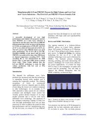
DC Characteristics<br />
Device and passive element parameters are m<strong>on</strong>itored at<br />
several in-process steps. Figure 6 shows the wafer average<br />
DC device parameters of G mp (Peak transc<strong>on</strong>ductance), I max<br />
(Drain current measured at V g = 0.4 V), and V gp (Gate<br />
voltage at G mp ) measured at 1 V drain bias for eighteen <strong>100</strong><br />
<strong>mm</strong> <str<strong>on</strong>g>InP</str<strong>on</strong>g> <str<strong>on</strong>g>HEMT</str<strong>on</strong>g> wafers fabricated over seven wafer lots.<br />
The wafer average is based up<strong>on</strong> a minimum of thirty sites<br />
measured across each <strong>100</strong> <strong>mm</strong> wafer. The measurements<br />
were made <strong>on</strong> devices with 80 µm periphery at the post<br />
nitride via 1 step.<br />
(b)<br />
Figure 4. End view SEM of the <str<strong>on</strong>g>InP</str<strong>on</strong>g> <str<strong>on</strong>g>0.1</str<strong>on</strong>g> µm T-gate <strong>on</strong> <strong>100</strong> <strong>mm</strong> wafer.<br />
(a) 30KX magnificati<strong>on</strong>. (b) 60KX magnificati<strong>on</strong>.<br />
Gmp (mS/<strong>mm</strong>) and Imax (mA/<strong>mm</strong>)<br />
<strong>100</strong>0<br />
1<br />
900<br />
0.9<br />
Gmp<br />
0.8<br />
800<br />
0.7<br />
700<br />
0.6<br />
600<br />
0.5<br />
500<br />
Imax<br />
0.4<br />
400<br />
0.3<br />
0.2<br />
300<br />
<str<strong>on</strong>g>0.1</str<strong>on</strong>g><br />
200<br />
Vgp<br />
0<br />
<strong>100</strong><br />
-<str<strong>on</strong>g>0.1</str<strong>on</strong>g><br />
0<br />
-0.2<br />
0 1 2 3 4 5 6 7 8 9 10111213141516171819<br />
Wafer number<br />
Vgp (V)<br />
40 µm<br />
Figure 6. Wafer average DC device parameters of G mp , I max , and V gp for<br />
eighteen <strong>100</strong> <strong>mm</strong> <str<strong>on</strong>g>InP</str<strong>on</strong>g> <str<strong>on</strong>g>HEMT</str<strong>on</strong>g> wafers. Devices have <str<strong>on</strong>g>0.1</str<strong>on</strong>g> µm gate length and<br />
80 µm periphery.<br />
Figure 5. SEM cross-secti<strong>on</strong> of the <str<strong>on</strong>g>InP</str<strong>on</strong>g> backside through via.<br />
Backside <str<strong>on</strong>g>Fabricati<strong>on</strong></str<strong>on</strong>g> Process<br />
In the backside process, the <strong>100</strong> <strong>mm</strong> <str<strong>on</strong>g>InP</str<strong>on</strong>g> substrates are<br />
b<strong>on</strong>ded to 109 <strong>mm</strong> sapphire substrates. The wafers are<br />
thinned to a final thickness of 75 µm (3-mil) using<br />
mechanical grinding. An RIE system is used to dry etch the<br />
backside through-substrate vias (See Figure 5) using a<br />
hydrogen bromide based gas mixture. The through vias<br />
From the data in Figure 6, the wafer average G mp is 800<br />
mS/<strong>mm</strong>, the wafer average I max is 545 mA/<strong>mm</strong>, and the<br />
wafer average V gp is <str<strong>on</strong>g>0.1</str<strong>on</strong>g> V. The higher G mp for recent<br />
wafers (Wafers 11-18 in Figure 6) is credited to improved<br />
gate length and recess width c<strong>on</strong>trol, and to reduced ohmic<br />
c<strong>on</strong>tact resistance. Within an individual wafer, the typical<br />
sigma for G mp , I max , and V gp is 66 mS/<strong>mm</strong>, 41 mA/<strong>mm</strong>, and<br />
0.06 V, respectively. DC device functi<strong>on</strong>al yield is typically<br />
greater than 95%. Device f t is in excess of 190 GHz.
RF Characteristics<br />
An example of <str<strong>on</strong>g>MMIC</str<strong>on</strong>g> performance <strong>on</strong> <strong>100</strong> <strong>mm</strong> <str<strong>on</strong>g>InP</str<strong>on</strong>g><br />
substrates is shown in Figure 7 for a 2-stage balanced Kaband<br />
LNA. This Ka-band LNA has noise figure less than<br />
2.4 dB and with greater than 17 dB associated gain over the<br />
frequency band 27-39 GHz. This performance is comparable<br />
to that achieved <strong>on</strong> the 75 <strong>mm</strong> <str<strong>on</strong>g>InP</str<strong>on</strong>g> <str<strong>on</strong>g>HEMT</str<strong>on</strong>g> process line at<br />
NGST [5]. RF yield across the <strong>100</strong> <strong>mm</strong> wafer based <strong>on</strong> a 3<br />
dB noise figure spec at 33 GHz was as high as 72% with 495<br />
out of 684 sites passing. The standard deviati<strong>on</strong> of noise<br />
figure and gain at 33 GHz across a wafer was 0.26 dB and<br />
0.84 dB, respectively. A micrograph of the 20-stage Ka-band<br />
LNA is shown in Figure 8.<br />
ACKNOWLEDGEMENTS<br />
The authors acknowledge P. Oliver, F. Yamada, R. To,<br />
B. Akiyama, and K. Padmanabhan for their c<strong>on</strong>tributi<strong>on</strong>s <strong>on</strong><br />
the development and characterizati<strong>on</strong> of the <strong>100</strong> <strong>mm</strong> <str<strong>on</strong>g>InP</str<strong>on</strong>g><br />
<str<strong>on</strong>g>HEMT</str<strong>on</strong>g> <str<strong>on</strong>g>MMIC</str<strong>on</strong>g> fabricati<strong>on</strong> process. The authors also<br />
acknowledge the labs and pers<strong>on</strong>nel in D1, MBE, EBL,<br />
backside, layout, and RF test.<br />
20<br />
4<br />
Gain (dB)<br />
18<br />
16<br />
14<br />
12<br />
10<br />
8<br />
6<br />
4<br />
2<br />
0<br />
0<br />
27 28 29 30 31 32 33 34 35 36 37 38 39<br />
Frequency (GHz)<br />
Figure 7. Noise figure and associated gain of a <str<strong>on</strong>g>0.1</str<strong>on</strong>g> µm <str<strong>on</strong>g>InP</str<strong>on</strong>g> <str<strong>on</strong>g>HEMT</str<strong>on</strong>g> Ka-band<br />
2-stage balanced LNA fabricated <strong>on</strong> <strong>100</strong> <strong>mm</strong> <str<strong>on</strong>g>InP</str<strong>on</strong>g> substrate.<br />
CONCLUSIONS<br />
We have successfully developed processes for fabricating<br />
<str<strong>on</strong>g>0.1</str<strong>on</strong>g> µm InGaAs/InAlAs/<str<strong>on</strong>g>InP</str<strong>on</strong>g> <str<strong>on</strong>g>HEMT</str<strong>on</strong>g> <str<strong>on</strong>g>MMIC</str<strong>on</strong>g>s <strong>on</strong> <strong>100</strong> <strong>mm</strong> <str<strong>on</strong>g>InP</str<strong>on</strong>g><br />
substrates. Manufacturability of <str<strong>on</strong>g>InP</str<strong>on</strong>g> <str<strong>on</strong>g>HEMT</str<strong>on</strong>g> <str<strong>on</strong>g>MMIC</str<strong>on</strong>g>s has<br />
been dem<strong>on</strong>strated in three core areas: MBE epitaxial<br />
material growth and in both fr<strong>on</strong>tside and backside<br />
processing. Good DC and RF electrical performance have<br />
been obtained with average G mp of 800 mS/<strong>mm</strong> and f t<br />
greater than 190 GHz and with acceptable yield. Additi<strong>on</strong>al<br />
characterizati<strong>on</strong> of the <str<strong>on</strong>g>InP</str<strong>on</strong>g> <str<strong>on</strong>g>HEMT</str<strong>on</strong>g> devices and W-band<br />
<str<strong>on</strong>g>MMIC</str<strong>on</strong>g>s are <strong>on</strong>-going. The scaling to <strong>100</strong> <strong>mm</strong> <str<strong>on</strong>g>InP</str<strong>on</strong>g> substrates<br />
and shared processes with the HBT and GaAs <str<strong>on</strong>g>HEMT</str<strong>on</strong>g><br />
technologies results in lower fabricati<strong>on</strong> costs. Further<br />
process optimizati<strong>on</strong> will enhance the robustness of the <strong>100</strong><br />
<strong>mm</strong> <str<strong>on</strong>g>InP</str<strong>on</strong>g> <str<strong>on</strong>g>HEMT</str<strong>on</strong>g> <str<strong>on</strong>g>MMIC</str<strong>on</strong>g>s. These factors will enable wider<br />
acceptance of <str<strong>on</strong>g>InP</str<strong>on</strong>g> <str<strong>on</strong>g>HEMT</str<strong>on</strong>g> technology for next generati<strong>on</strong><br />
applicati<strong>on</strong>s.<br />
3.5<br />
3<br />
2.5<br />
2<br />
1.5<br />
1<br />
0.5<br />
Noise figure (dB)<br />
Figure 8. Micrograph of a Ka-band 2-staged balanced <str<strong>on</strong>g>MMIC</str<strong>on</strong>g> LNA<br />
operating over 27-39 GHz fabricated by <str<strong>on</strong>g>0.1</str<strong>on</strong>g> µm <str<strong>on</strong>g>InP</str<strong>on</strong>g> <str<strong>on</strong>g>HEMT</str<strong>on</strong>g> technology <strong>on</strong><br />
<strong>100</strong> <strong>mm</strong> <str<strong>on</strong>g>InP</str<strong>on</strong>g> substrate.<br />
REFERENCES<br />
[1] M. Wojtowicz, R. Lai, D.C. Streit, G.I. Ng, T.R. Block, K.L. Tan, P.H.<br />
Liu, A.K. Freudenthal, R.M. Dia, <str<strong>on</strong>g>0.1</str<strong>on</strong>g>0 µm graded InGaAs channel <str<strong>on</strong>g>InP</str<strong>on</strong>g><br />
<str<strong>on</strong>g>HEMT</str<strong>on</strong>g> with 305 GHz f t and 340 GHz f max , IEEE Electr<strong>on</strong> Device<br />
Letters, Vol. 15, No. 11, pp. 477-479, Nov. 1994.<br />
[2] K. Shinohara, Y. Yamashita, A. Endoh, K. Hikosaka, T. Matsui, T.<br />
Mimura, and S. Hiyamizu, Ultrahigh-Speed Pseudomorphic<br />
InGaAs/InAlAs <str<strong>on</strong>g>HEMT</str<strong>on</strong>g>s With 400-GHz Cutoff Frequency, IEEE<br />
Electr<strong>on</strong> Device Letters, Vol. 22, No. 11, pp. 507-509, Nov. 2001.<br />
[3] D. Streit, R. Lai, A. Oki, and A. Gutierrez-Aitken, <str<strong>on</strong>g>InP</str<strong>on</strong>g> <str<strong>on</strong>g>HEMT</str<strong>on</strong>g> and HBT<br />
Applicati<strong>on</strong>s Bey<strong>on</strong>d 200 GHz, Electr<strong>on</strong> Devices for Microwave and<br />
Optoelectr<strong>on</strong>ic Applicati<strong>on</strong>s, 2002. The 10th IEEE Internati<strong>on</strong>al<br />
Symposium On, pp. 11-14, Nov. 2002.<br />
[4] Y.C. Chou, D. Leung, R. Lai, R. Grundbacher, M. Barsky, Q. Kan, R.<br />
Tsai, D. Eng, M. Wojtowicz, T. Block, P.H. Liu, S. Ols<strong>on</strong>, A. Oki, D.C.<br />
Streit, <str<strong>on</strong>g>0.1</str<strong>on</strong>g>/spl mu/m InGaAs/InAlAs/<str<strong>on</strong>g>InP</str<strong>on</strong>g> <str<strong>on</strong>g>HEMT</str<strong>on</strong>g> <str<strong>on</strong>g>MMIC</str<strong>on</strong>g>s - a flight<br />
qualified technology, Gallium Arsenide Integrated Circuit (GaAs IC)<br />
Symposium, pp.77-80, 2002.<br />
[5] Y.C. Chou, D. Leung, R. Lai, J. Scarpulla, M. Barsky, R. Grundbacher,<br />
D. Eng, P.H. Liu, A. Oki and D.C. Streit, High Reliability of <str<strong>on</strong>g>0.1</str<strong>on</strong>g> <strong>mm</strong><br />
InGaAs/InAlAs/<str<strong>on</strong>g>InP</str<strong>on</strong>g> <str<strong>on</strong>g>HEMT</str<strong>on</strong>g> <str<strong>on</strong>g>MMIC</str<strong>on</strong>g>s <strong>on</strong> 3-inch <str<strong>on</strong>g>InP</str<strong>on</strong>g> Producti<strong>on</strong> Process,<br />
2001 IEEE GaAs Digest, pp. 174-177, 2001.<br />
ACRONYMS<br />
<str<strong>on</strong>g>HEMT</str<strong>on</strong>g>: High Electr<strong>on</strong> Mobility Transistor<br />
LNA: Low Noise Amplifier<br />
MBE: Molecular Beam Epitaxy<br />
<str<strong>on</strong>g>MMIC</str<strong>on</strong>g>: M<strong>on</strong>olithic Microwave Integrated Circuit<br />
MIMCAP: Metal-Insulator-Metal Capacitor<br />
NRE: N<strong>on</strong>-Recurring Engineering<br />
RIE: Reactive I<strong>on</strong> Etch