
You also want an ePaper? Increase the reach of your titles
YUMPU automatically turns print PDFs into web optimized ePapers that Google loves.
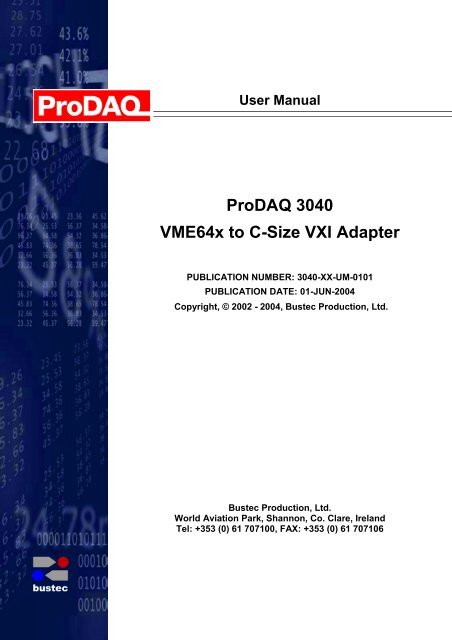
<strong>User</strong> <strong>Manual</strong><br />
<strong>ProDAQ</strong> <strong>3040</strong><br />
VME64x to C-Size VXI Adapter<br />
PUBLICATION NUMBER: <strong>3040</strong>-XX-UM-0101<br />
PUBLICATION DATE: 01-JUN-2004<br />
Copyright, © 2002 - 2004, <strong>Bustec</strong> Production, Ltd.<br />
<strong>Bustec</strong> Production, Ltd.<br />
World Aviation Park, Shannon, Co. Clare, Ireland<br />
Tel: +353 (0) 61 707100, FAX: +353 (0) 61 707106
PROPRIETARY NOTICE<br />
This document and the technical data herein disclosed, are proprietary to <strong>Bustec</strong><br />
Production Ltd., and shall not, without express written permission of <strong>Bustec</strong><br />
Production Ltd, be used, in whole or in part to solicit quotations from a competitive<br />
source or used for manufacture by anyone other than <strong>Bustec</strong> Production Ltd. The<br />
information herein has been developed at private expense, and may only be used<br />
for operation and maintenance reference purposes or for purposes of engineering<br />
evaluation and incorporation into technical specifications and other documents,<br />
which specify procurement of products from <strong>Bustec</strong> Production Ltd. This document<br />
is subject to change without further notification. <strong>Bustec</strong> Production Ltd. Reserve the<br />
right to change both the hardware and software described herein.
<strong>ProDAQ</strong> <strong>3040</strong> 6U VME64x to C-Size VXI Adapter <strong>User</strong> <strong>Manual</strong><br />
<strong>3040</strong>-XX-UM<br />
Table of Contents<br />
1. THEORY OF OPERATION.......................................................................................... 5<br />
1.1 GENERAL................................................................................................................ 5<br />
1.2 VME-VXI MASTER CHANNEL.................................................................................... 5<br />
1.3 VXI-VME SLAVE CHANNEL....................................................................................... 5<br />
1.4 VXI TO VME ADDRESS SPACE MAPPING.................................................................... 7<br />
1.5 VXI-TO-VME INTERRUPT FORWARDING.................................................................. 11<br />
1.6 VME-TO-VXI INTERRUPT FORWARDING.................................................................. 11<br />
1.7 UTILITY BUS.......................................................................................................... 12<br />
1.8 AUTO SLOT-0 DETECTION AND MODID/CLK10 ....................................................... 12<br />
1.9 AUTO SYSTEM CONTROLLER DETECTION ................................................................ 13<br />
2. INSTALLATION AND CONFIGURATION................................................................. 15<br />
2.1 PREPARING THE VME BOARD ................................................................................ 15<br />
2.2 CONFIGURING THE PRODAQ <strong>3040</strong> ADAPTER.......................................................... 15<br />
2.2.1 Logical Address ........................................................................................... 16<br />
2.2.2 VXI to VME Address Space Mapping .......................................................... 17<br />
3. REGISTER DESCRIPTION ....................................................................................... 21<br />
3.1 ADDRESS MAP AND REGISTERS.............................................................................. 21<br />
3.2 REGISTER DETAILS................................................................................................ 22<br />
3.2.1 ID Register................................................................................................... 22<br />
3.2.2 LogAdr ......................................................................................................... 22<br />
3.2.3 DevType ...................................................................................................... 22<br />
3.2.4 Status .......................................................................................................... 23<br />
3.2.5 Control ......................................................................................................... 24<br />
3.2.6 Offset........................................................................................................... 24<br />
3.2.7 MODID......................................................................................................... 24<br />
3.2.8 VMEOffset ................................................................................................... 25<br />
3.2.9 VXIControl ................................................................................................... 25<br />
3.2.10 VMEControl ................................................................................................. 26<br />
3.2.11 EEPROMData ............................................................................................. 26<br />
3.2.12 EEPROMCtrl ............................................................................................... 27<br />
3.2.13 TrigStatus .................................................................................................... 27<br />
3.2.14 TrigIntMask.................................................................................................. 27<br />
3.2.15 TrigControl................................................................................................... 29<br />
3.2.16 TrigIntMode ................................................................................................. 29<br />
3.2.17 IRQDir.......................................................................................................... 30<br />
3.2.18 SerNumHigh ................................................................................................ 30<br />
3.2.19 SerNumLow................................................................................................. 30<br />
APPENDIX A. EEPROM PROGRAMMING FLOW CHARTS...................................... 31<br />
Copyright, © 2002 <strong>Bustec</strong> Production Ltd. Page 3 of 34
<strong>3040</strong>-XX-UM<br />
<strong>ProDAQ</strong> <strong>3040</strong> 6U VME64x to C-Size VXI Adapter <strong>User</strong> <strong>Manual</strong><br />
Page 4 of 34<br />
Copyright, © 2002 <strong>Bustec</strong> Production Ltd.
<strong>ProDAQ</strong> <strong>3040</strong> 6U VME64x to C-Size VXI Adapter <strong>User</strong> <strong>Manual</strong><br />
<strong>3040</strong>-XX-UM<br />
1. Theory of Operation<br />
The <strong>ProDAQ</strong> <strong>3040</strong> 6U VME64x to C-Size VXIbus Adapter allows the usage of 6U VMEbus<br />
boards in a C-Size VXIbus system. It translates VMEbus cycles into VXIbus cycles and<br />
vice versa. In addition it houses the extensions necessary for VXIbus devices, as there are<br />
the configuration registers, a trigger and extended interrupt interface, MODID support and<br />
the 10 MHz clock generation.<br />
It forwards all VME master cycles transparently to the VXIbus, allowing a VMEbus master<br />
the full access to the VXIbus. On the VXIbus it allows the full integration of the module in<br />
the VXIbus resource management by providing a set of VXIbus compatible configuration<br />
registers and a configurable translation window in the VXIbus A24 or A32 address space.<br />
Accesses to this translation window are forwarded to the VMEbus module’s A16, A24, A32<br />
or CR/CSR space.<br />
Programmable interrupt, trigger and MODID support (both detection and generation), 10<br />
MHz clock generation and auto-Slot0 detection allow the board to be used as an<br />
embedded controller in Slot-0 and non-Slot-0 applications.<br />
1.1 General<br />
The <strong>ProDAQ</strong> <strong>3040</strong> adapter can be placed in both slot-0 and non-slot-0 positions and<br />
accepts both master and slave VME boards. It forwards all VME master cycles<br />
transparently to the VXIbus through the VME-VXI master channel, and translates<br />
accesses to the configured address range through the VXI-VME slave channel.<br />
1.2 VME-VXI master channel<br />
The cycles generated by the VME master are directly forwarded to the VXI bus. Both<br />
address modifier and addresses stay unchanged during the conversion of the cycle. The<br />
cycles are forwarded at full speed and the only delay is caused by the propagation delay of<br />
the buffers. For the VME-VXI master channel the following cycles are supported:<br />
A16: D08(EO), D16, D32<br />
A24: D08(EO), D08(EO)BLT, D16, D16BLT, D32, D32BLT, MBLT<br />
A32: D08(EO), D08(EO)BLT, D16, D16BLT, D32, D32BLT, MBLT<br />
1.3 VXI-VME slave channel<br />
The VXI-VME slave channel allows the accesses to the on-board register resources and to<br />
the resources of the VME board. The cycles performed in the A16 address space are<br />
directed to the adapter’s registers. The cycles performed in the A24 or A32 are mapped to<br />
the selected address space of the VMEbus. The following cycles are supported:<br />
A16: D08(EO), D16, D32<br />
A24: D08(EO), D08(EO)BLT, D16, D16BLT, D32, D32BLT, MBLT<br />
A32: D08(EO), D08(EO)BLT, D16, D16BLT, D32, D32BLT, MBLT<br />
The base address of the VXIbus configuration registers in A16 address space is set by the<br />
logical address switch or is assigned dynamically. The base address and size of the<br />
window in A24 or A32 is configured as follows:<br />
Copyright, © 2002 <strong>Bustec</strong> Production Ltd. Page 5 of 34
<strong>3040</strong>-XX-UM<br />
<strong>ProDAQ</strong> <strong>3040</strong> 6U VME64x to C-Size VXI Adapter <strong>User</strong> <strong>Manual</strong><br />
VME-VXI Master<br />
Channel<br />
VMEbus<br />
Master<br />
VXIbus<br />
Slave<br />
VXi-VME<br />
Slave<br />
Channel<br />
Configuration<br />
Registers<br />
/<br />
Control Logic<br />
V<br />
M<br />
E<br />
b<br />
u<br />
EEPROM<br />
VXIbus / FP<br />
Trigger<br />
V<br />
X<br />
I<br />
b<br />
u<br />
s<br />
VXI-to-VME<br />
Interrupt Forwarding<br />
Tigger<br />
Interrupter<br />
s<br />
VME-to-VXI<br />
Interrupt Forwarding<br />
MODID<br />
CLK10<br />
P2<br />
Connector<br />
Transition<br />
Board<br />
HDD<br />
optional<br />
Slot-0<br />
Detection<br />
Bus timer<br />
Auto-Syscon<br />
Detection<br />
Figure 1 - <strong>ProDAQ</strong> <strong>3040</strong> Block Diagram<br />
Page 6 of 34<br />
Copyright, © 2002 <strong>Bustec</strong> Production Ltd.
<strong>ProDAQ</strong> <strong>3040</strong> 6U VME64x to C-Size VXI Adapter <strong>User</strong> <strong>Manual</strong><br />
<strong>3040</strong>-XX-UM<br />
1.4 VXI to VME address space mapping<br />
The <strong>ProDAQ</strong> <strong>3040</strong> adapter is a register based VXIbus device. It features the standard set<br />
of VXIbus configuration registers and can be configured to decode additionally an address<br />
range in the VXIbus A24 or A32 address range. Accesses to this address range are<br />
translated into a configurable address range on the VMEbus.<br />
VXIbus<br />
Configuration<br />
Register<br />
A16 Address Range<br />
Size = 64 Bytes<br />
Base = 0xC000 + (LA * 64)<br />
A16, A24, CR/CSR or A32<br />
Address Range<br />
(VME Control Register)<br />
Size = As VXI Addr. Range<br />
Base = VME_BASE Register<br />
A24 or A32 Address Range<br />
(ID register)<br />
Size = Programmable<br />
(Device Type Register)<br />
Base = Resource Manager<br />
(set during run-time)<br />
VMEbus<br />
VXIbus<br />
Figure 2 - Available Address Ranges<br />
The address range for the access to the VXIbus configuration registers is 64 bytes in size<br />
and its base address is either set by statically the logical address switch or dynamically by<br />
the resource manager.<br />
The configuration registers contain the information about the address range (on the<br />
VXIbus) of the module to be used by the resource manager. On the <strong>ProDAQ</strong> <strong>3040</strong> this<br />
information is programmable and stored in an EEPROM and is also used during hardware<br />
initialization to configure the VXI-to-VME address mapping.<br />
The ID register at offset 0 contains the information, whether the board is set for A16 only,<br />
A16/A24 or A16/A32 address space. If the board is programmed for A16 only, the VXI-to-<br />
VME address mapping is turned off and only the access to the configuration registers in<br />
the A16 address space is possible. If it is programmed for A16/A24 address space, the<br />
address mapping is enabled for mapping a range in the A24 VXIbus address space to the<br />
specified VME address space. If the board is set for A16/A32 address space, the address<br />
mapping is enabled for mapping a range in the A32 VXIbus address space to the specified<br />
VME address space.<br />
The Device Type register at offset 2 in the VXIbus configuration register contains the<br />
information of the memory size a VXIbus module requires. This information is used by the<br />
VXIbus resource manager to arrange the different memory ranges of the VXIbus boards in<br />
a system in the available space. It also determines the size of the range that is mapped to<br />
the VME address space.<br />
The Offset register determines the base address of the decoded VXIbus A24 or A32<br />
address range and is set during run-time by the resource manager.<br />
Copyright, © 2002 <strong>Bustec</strong> Production Ltd. Page 7 of 34
<strong>3040</strong>-XX-UM<br />
<strong>ProDAQ</strong> <strong>3040</strong> 6U VME64x to C-Size VXI Adapter <strong>User</strong> <strong>Manual</strong><br />
The VME Control register contains the information, which address range on the VMEbus<br />
the accesses to the configured VXIbus address range should be mapped to. The VME<br />
Offset register determines the base address of the VMEbus address range.<br />
VXI Address A[23..16] A[15..0]<br />
compared with<br />
Offset register<br />
VMEbase reg.<br />
D[15..8]<br />
D[------]<br />
used for<br />
VME Address A[------] A[15..0]<br />
Figure 3 - VXIbus A24 to VMEbus A16 mapping<br />
Figure 3 shows the VXIbus A24 to VME A16 mapping. The only usable size of the mapped<br />
range is 64k due to the minimum memory space size in A24 as defined by the VXIbus<br />
standard.<br />
VXI Address A[31..16] A[15..0]<br />
compared with<br />
Offset register<br />
VMEbase reg.<br />
D[15..0]<br />
D[------]<br />
used for<br />
VME Address A[------] A[15..0]<br />
Figure 4 - VXIbus A32 to VMEbus A16 mapping<br />
Figure 4 shows the VXIbus A32 to VMEbus A16 mapping. As before, the only usable size<br />
of the mapped range is 64k due to the minimum memory space size as defined by the<br />
VXIbus standard.<br />
Page 8 of 34<br />
Copyright, © 2002 <strong>Bustec</strong> Production Ltd.
<strong>ProDAQ</strong> <strong>3040</strong> 6U VME64x to C-Size VXI Adapter <strong>User</strong> <strong>Manual</strong><br />
<strong>3040</strong>-XX-UM<br />
VXI Address A[23..(23-m)] A[(23-m-1)..0]<br />
compared with<br />
Offset register<br />
VMEbase reg.<br />
D[15..(15-m)]<br />
D[15..(15-m)]<br />
used for<br />
VME Address A[23..(23-m)] A[(23-m-1)..0]<br />
Figure 5 - VXIbus A24 to VMEbus A24 mapping<br />
Figure 5 shows the VXIbus A24 to VMEbus A24 mapping. The size of the mapped range<br />
can be 64 kByte to 8 MByte (m = 7..0).<br />
VXI Address A[31..(31-m)] A[(31-m-1)..0]<br />
compared with<br />
Offset register<br />
VMEbase reg.<br />
D[15..(15-m)]<br />
D[15..(23-m)]<br />
used for<br />
VME Address A[23..(31-m)] A[(31-m-1)..0]<br />
Figure 6 - VXIbus A32 to VMEbus A24 mapping<br />
Figure 6 shows the VXIbus A32 to VMEbus A24 mapping. The size of the mapped range<br />
can be 64 kByte to 16 MByte (m = 15..7). If it is 16 MByte, the content of the VMEbase<br />
register is not used, because the whole A24 address range is mapped.<br />
Copyright, © 2002 <strong>Bustec</strong> Production Ltd. Page 9 of 34
<strong>3040</strong>-XX-UM<br />
<strong>ProDAQ</strong> <strong>3040</strong> 6U VME64x to C-Size VXI Adapter <strong>User</strong> <strong>Manual</strong><br />
VXI Address A[23..(23-m)] A[(23-m-1)..0]<br />
compared with<br />
Offset register<br />
VMEbase reg.<br />
D[15..(15-m)]<br />
D[15..(7-m)]<br />
used for<br />
VME Address A[31..(23-m)] A[(23-m-1)..0]<br />
Figure 7 - VXIbus A24 to VMEbus A32 mapping<br />
Figure 7 shows the VXIbus A24 to VMEbus A32 mapping. The size of the mapped range<br />
can be 64 kByte to 8 MByte (m = 7..0).<br />
VXI Address A[31..(31-m)] A[(31-m-1)..0]<br />
compared with<br />
Offset register<br />
VMEbase reg.<br />
D[15..(15-m)]<br />
D[15..(15-m)]<br />
used for<br />
VME Address A[31..(31-m)] A[(31-m-1)..0]<br />
Figure 8 - VXIbus A32 to VMEbus A32 mapping<br />
Figure 8 shows the VXIbus A32 to VMEbus A32 mapping. The size of the mapped range<br />
can be 64 kByte to 2 GByte (m = 15..0).<br />
Page 10 of 34<br />
Copyright, © 2002 <strong>Bustec</strong> Production Ltd.
<strong>ProDAQ</strong> <strong>3040</strong> 6U VME64x to C-Size VXI Adapter <strong>User</strong> <strong>Manual</strong><br />
<strong>3040</strong>-XX-UM<br />
1.5 VXI-to-VME Interrupt Forwarding<br />
The VXI-to-VME interrupt forwarding concerns the situation when the interrupt handler is<br />
located on the VME board and interrupters are located on the VXIbus (including the<br />
adapter’s own interrupter). In this situation there is a need to send an interrupt that<br />
happened on the VXIbus to the VMEbus. The adapter maps directly the VXIbus interrupts<br />
to the VMEbus interrupts (VXI IRQ1 to VME IRQ1, VXI IRQ2 to VME IRQ2, etc).<br />
Before the interrupt signal can be forwarded from the VXIbus to the VMEbus, it has to be<br />
enabled by using the IRQDIR[7..1] bits from IRQDir register. Only the interrupts, which are<br />
handled by the VME Interrupt Handler, have to be forwarded and only these interrupts<br />
should be enabled using IRQDIR bits.<br />
Most of the VME Interrupt Handlers generate D08(O) cycles during interrupt acknowledge<br />
cycle but D16 and D32 are allowed by the VME64 standard as well. On the other side the<br />
VXI standard specifies the status/ID of up to 32-bit width and every interrupter is forced to<br />
respond to any of D08, D16 or D32 cycles with the appropriate status/ID width.<br />
To fulfill the VXI and VME standard requirements, the following scheme has been<br />
implemented in the VXI-to-VME interrupt forwarding channel: the VME interrupt handler<br />
can initiate any of the three cycles D08(O), D16 or D32. In response to any of these cycles<br />
the interrupt forwarder will always generate a D32 cycle on the VXIbus. When the<br />
interrupters status/ID is ready, only the part will be forwarded to the VMEbus, which is<br />
requested by the handler (byte, word or long word).<br />
The status/ID forwarded to the VME side is defined in the following way:<br />
Status/ID bits forwarded<br />
from VXI to VME bus<br />
D[7..0]<br />
D[15..0]<br />
D[31..0]<br />
If VME Interrupt<br />
Handler is<br />
D08(O)<br />
D16<br />
D32<br />
Independently of this the whole 32-bit status/ID is latched in the adapter’s memory and can<br />
be read by the ISR. There is a separate location for every interrupt level to store the<br />
status/ID. Forwarding the interrupt for the given level becomes disabled after the status/ID<br />
is latched during interrupt acknowledge cycle. It can be only enabled by reading out the<br />
latched status/ID.<br />
1.6 VME-to-VXI Interrupt Forwarding<br />
The VME-to-VXI interrupt forwarding concerns the situation when the interrupt handler is<br />
located on the VXIbus and the interrupter is located on the VMEbus. In this situation there<br />
is a need to forward an interrupt that happened on the VMEbus to the VXIbus. The adapter<br />
maps directly the VMEbus interrupts to the VXIbus interrupts (VME IRQ1 to VXI IRQ1,<br />
VME IRQ2 to VXI IRQ2, etc).<br />
Before the interrupt signal can be forwarded from the VMEbus to the VXIbus it has to be<br />
enabled using IRQDIR[7..1] bits from IRQDir register. The VXI Interrupt Handler generates<br />
D16 or D32 cycles during interrupt acknowledge cycle. On the other side the VME<br />
standard specifies that every interrupter (D08, D16 or D32) is forced to respond to D32<br />
cycle with the appropriate status/ID width.<br />
Copyright, © 2002 <strong>Bustec</strong> Production Ltd. Page 11 of 34
<strong>3040</strong>-XX-UM<br />
<strong>ProDAQ</strong> <strong>3040</strong> 6U VME64x to C-Size VXI Adapter <strong>User</strong> <strong>Manual</strong><br />
To fulfill the requirements, the following scheme has been implemented for the VME-to-<br />
VXI interrupt forwarding channel: the VXI interrupt handler can initiate either D16 or D32.<br />
In the response to any of these cycles the interrupt forwarder will always generate D32<br />
cycle on the VMEbus. The status forwarded to the VXI side will be 16-bit always and will<br />
be composed of the adapter’s logical address and the eight lower bits of the VME<br />
status/ID.<br />
The status/ID forwarded to the VXI side will always be 16-bit and is defined in the following<br />
way:<br />
Forwarded<br />
16-bit VXIbus<br />
Status/ID<br />
Is composed<br />
of<br />
Description<br />
D[7..0] LA[7..0] Adapter’s Logical Address<br />
D[15..8] D[7..0] (VME) Lower 8 bits of VME Status/ID<br />
The VME-to-VXI interrupt forwarding will not become disabled after the status/ID is latched<br />
during interrupt acknowledge cycle.<br />
1.7 Utility Bus<br />
The <strong>ProDAQ</strong> <strong>3040</strong> Adapter allows generating either a soft reset or a VXIbus SYSRESET.<br />
The soft reset is generated using the RESET bit in the Control register. It restarts the<br />
adapters self test and disables the MODID drivers.<br />
The VXIbus SYSRESET is generated by using the SYSRESET bit in the VXIcontrol<br />
register and is send to the VXIbus only to allow to reset the VXIbus under software<br />
control.<br />
The SYSCLK isignal s taken from the VME board if the module is system controller (see<br />
below). The SYSCLK signal is not generated on the adapter. If the module is not the<br />
system controller, then the SYSCLK is propagated from the VXIbus to the VMEbus.<br />
The SYSFAIL driver is implemented as a bi-directional signal driver that allows the VME<br />
board to monitor and drive this line. The ACFAIL signal is forwarded from the VXIbus to<br />
the VMEbus so that the VME board can monitor this signal.<br />
1.8 Auto Slot-0 Detection and ModID/CLK10<br />
The adapter automatically detects whether he is placed in slot 0 (the leftmost slot in a<br />
VXIbus mainframe) and enables or disables the CLK10 and MODID lines accordingly. The<br />
CLK10 signal can be configured to be either generated from the on-board oscillator or to<br />
be sourced from an external signal via the front panel connector. The front-panel input for<br />
the CLK10 signal accepts a standard TTL signal.<br />
Page 12 of 34<br />
Copyright, © 2002 <strong>Bustec</strong> Production Ltd.
<strong>ProDAQ</strong> <strong>3040</strong> 6U VME64x to C-Size VXI Adapter <strong>User</strong> <strong>Manual</strong><br />
<strong>3040</strong>-XX-UM<br />
1.9 Auto System Controller Detection<br />
The adapter supports auto system controller detection on the VXIbus. The result is then<br />
carried forward to the VMEbus to allow auto system controller detection on the VME<br />
board. Except of the bus timer the adapter does not implement any functionality of a<br />
system controller on its own. It only carries the system controller functionality from the<br />
VME board to the VXIbus, if the adapter is placed in the system controller slot.<br />
Copyright, © 2002 <strong>Bustec</strong> Production Ltd. Page 13 of 34
<strong>3040</strong>-XX-UM<br />
<strong>ProDAQ</strong> <strong>3040</strong> 6U VME64x to C-Size VXI Adapter <strong>User</strong> <strong>Manual</strong><br />
Page 14 of 34<br />
Copyright, © 2002 <strong>Bustec</strong> Production Ltd.
<strong>ProDAQ</strong> <strong>3040</strong> 6U VME64x to C-Size VXI Adapter <strong>User</strong> <strong>Manual</strong><br />
<strong>3040</strong>-XX-UM<br />
2. Installation and Configuration<br />
2.1 Preparing the VME Board<br />
To use a VME board in a VXIbus system, simply connect the board to the adapter using<br />
the P1 and P2 connector of the VME board and the female connectors J300 and J301 of<br />
the <strong>ProDAQ</strong> <strong>3040</strong> Adapter.<br />
The adapter supports automatic system controller detection on the VME side. None the<br />
less this feature might not work with some boards, so that it could be necessary to<br />
configure the VME board to be fixed either system controller or not, depending on the<br />
usage in the VXIbus system.<br />
If the VME board features a VME slave for registers or local memory, the adapter must be<br />
set up to support a VXI to VME address translation window. Please refer to section 2.2.2<br />
how to configure the adapter for this. The adapter supports, in accordance to the VXI<br />
standard, one window, which can translate a A24 or A32 access on the VXI side to a A16<br />
or A24 or A32 access on the VME side (see section 1.3 and 1.4).<br />
2.2 Configuring the <strong>ProDAQ</strong> <strong>3040</strong> Adapter<br />
The <strong>ProDAQ</strong> <strong>3040</strong> Adapter can be configured by writing to the VXIbus configuration<br />
registers located in A16 address space of the VXIbus(see section 3). Do be able to write to<br />
those registers, the adapter must be configured either to use a static logical address or the<br />
resource manager must be used to assign dynamically a logical address to the adapter<br />
(see section 2.2.1 for details). Any master on the VXIbus, as well as a VME master<br />
located on the adapter (because of the transparent forwarding of VME master cycles to the<br />
VXIbus done by the adapter), can then access the configuration registers.<br />
If the system supports the VISA standard, a session can be opened to the adapter using<br />
the standard viOpen() call, as for example (using logical address 2):<br />
ViSession rm_session;<br />
ViSession session;<br />
ViStatus status;<br />
status = viOpenDefaultRM (&rm_session);<br />
status = viOpen (rm_session, "VXI0::2::INSTR", VI_NULL, VI_NULL, &session);<br />
The register offsets as specified in Table 1 can then directly be used in the viIn() and<br />
viOut() calls to access the configuration registers:<br />
Copyright, © 2002 <strong>Bustec</strong> Production Ltd. Page 15 of 34
<strong>3040</strong>-XX-UM<br />
<strong>ProDAQ</strong> <strong>3040</strong> 6U VME64x to C-Size VXI Adapter <strong>User</strong> <strong>Manual</strong><br />
ViBusAddress offset;<br />
ViUInt16 value;<br />
offset = (ViBusAddress) 0x30; /* TrigStatus register */<br />
status = viIn16 (session, VI_A16_SPACE, offset, &value);<br />
If the system supports only bus addresses, the address of a register must be calculated<br />
using:<br />
address = 49152 + (LA ∗ 64) + offset<br />
where 49152 is the base address for the configuration register space according to the<br />
VXIbus standard, LA is the logical address the adapter is set to, and offset is a register<br />
offset as specified in Table 1. The calculated address is in the A16 address space and the<br />
registers can be accessed using either user or supervisory accesses as well as either<br />
program or data accesses.<br />
The following registers can be configured permanently using the on-board EEPROM.<br />
Using the algorithms as shown in Appendix A, the values stored in the EEPROM can be<br />
changed and will be used to initialize the registers after a power-on or hard reset.<br />
Register<br />
EEPROM offset<br />
ID 0<br />
DevType (for LA 0) 1<br />
DevType (LAs 1..255) 2<br />
VMEOffset 3<br />
VMEControl 4<br />
Attention:<br />
After changing the values in the EEPROM, a hard reset is necessary for<br />
the new values to become effective !<br />
2.2.1 Logical Address<br />
The <strong>ProDAQ</strong> <strong>3040</strong> Adapter can operate as either a Slot-0 controller or as a standard<br />
VXIbus device (non-Slot-0). When the <strong>ProDAQ</strong> <strong>3040</strong> is operated as the Slot-0 controller, it<br />
must be located in the left-most slot (slot “0“) of a VXIbus System Specification Rev 1.3 (or<br />
higher) compatible VXIbus mainframe and be set for logical address zero (0). If the<br />
<strong>ProDAQ</strong> <strong>3040</strong> is operated as a non-Slot-0, it may be located in any other slot and the<br />
logical address can be set to any value between 1 and 255.<br />
Figure 9 shows the location of the logical address switch on the <strong>ProDAQ</strong> <strong>3040</strong>. Set each<br />
switch to ‘Off’ for a logical one (1) and to ‘On’ for a logical zero (0). The picture shows the<br />
address switch set to logical address zero (0).<br />
If the <strong>ProDAQ</strong> <strong>3040</strong> is used in a non-slot-0 position, it can be either statically or<br />
dynamically configured. To configure it statically, the logical address switch must be set to<br />
a value between 1 and 254. This determines the logical address of the module<br />
permanently and can only be altered by changing the setting of the logical address switch.<br />
Page 16 of 34<br />
Copyright, © 2002 <strong>Bustec</strong> Production Ltd.
<strong>ProDAQ</strong> <strong>3040</strong> 6U VME64x to C-Size VXI Adapter <strong>User</strong> <strong>Manual</strong><br />
<strong>3040</strong>-XX-UM<br />
To configure the <strong>ProDAQ</strong> <strong>3040</strong> dynamically, the logical address switch must be set to 255.<br />
The resource manager will use the VXIbus MODID lines to access and configure the<br />
board, and assigns a logical address during run-time.<br />
LSB<br />
MSB<br />
1<br />
2<br />
3<br />
4<br />
5<br />
6<br />
7<br />
8<br />
log. "1" log. "0"<br />
LSB<br />
MSB<br />
1<br />
2<br />
3<br />
4<br />
5<br />
6<br />
7<br />
8<br />
log. "1" log. "0"<br />
VXIbus Connectors<br />
Solder Side<br />
VMEbus Connectors<br />
Figure 9 - Logical Address Switch Location<br />
2.2.2 VXI to VME Address Space Mapping<br />
The <strong>ProDAQ</strong> <strong>3040</strong> Adapter can be configured to forward slave accesses to an address<br />
range in VXIbus A24 or A32 to an address range in A16 or A24 or A32 in the VME space.<br />
This is done by writing register settings to the on-board EEPROM, from where they will be<br />
used after power-on or a hard reset to initialize the configuration registers.<br />
To set up the address space mapping, use the following steps:<br />
1. Select an address space in VXI<br />
The mapped address range can be located in the VXIbus A24 address space or the<br />
VXIbus A32 address space. This is configured by setting the adapter to be either a<br />
Copyright, © 2002 <strong>Bustec</strong> Production Ltd. Page 17 of 34
<strong>3040</strong>-XX-UM<br />
<strong>ProDAQ</strong> <strong>3040</strong> 6U VME64x to C-Size VXI Adapter <strong>User</strong> <strong>Manual</strong><br />
"A16/A24" device, a "A16/A32" device or a "A16 only" device. This information is located in<br />
the ID register (see 3.2.1 ID Register). Because the ID register content is initialized from<br />
the value stored in the EEPROM at address 0, the information stored there must be<br />
altered by using the algorithms shown in Appendix A.<br />
To change the value, read first the EEPROM contents at address 0. To map an address<br />
range in the VXIbus A32 address space, set the bits 13 and 12 of the 16-bit word read to<br />
zero ("0") and one ("1"). To map an address range in the VXIbus A24 address space, set<br />
bits 13 and 12 both to zero ("0"). To disable any address mapping, set bits 13 and 12 both<br />
to one ("1"). Store the changed value at EEPROM address zero.<br />
2. Specify the size of the mapped range<br />
The size of the mapped range is determined by the ReqMemory field in the DevType<br />
register. Valid values for this field are:<br />
VXI Address Space VME Address Space Size ReqMemory Bits<br />
A24 A16, A24, A32 64 kB 0111<br />
A24 A24, A32 128 kB 0110<br />
A24 A24, A32 256 kB 0101<br />
A24 A24, A32 512 kB 0100<br />
A24 A24, A32 1024 kB 0011<br />
A24 A24, A32 2048 kB 0010<br />
A24 A24, A32 4096 kB 0001<br />
A24 A24, A32 8192 kB 0000<br />
A32 A16, A24, A32 64 kB 1111<br />
A32 A24, A32 128 kB 1110<br />
A32 A24, A32 256 kB 1101<br />
A32 A24, A32 512 kB 1100<br />
A32 A24, A32 1024 kB 1011<br />
A32 A24, A32 2048 kB 1010<br />
A32 A24, A32 4096 kB 1001<br />
A32 A24, A32 8192 kB 1000<br />
A32 A24, A32 16384 kB 0111<br />
A32 A32 32 MB 0110<br />
A32 A32 64 MB 0101<br />
A32 A32 128 MB 0100<br />
A32 A32 256 MB 0011<br />
A32 A32 512 MB 0010<br />
A32 A32 1024 MB 0001<br />
A32 A32 2048 MB 0000<br />
As before, read the corresponding value from the EEPROM (DevType is address 1 and<br />
2), modify the bits for the ReqMemory field and store the value back into the EEPROM. In<br />
the case of the DevType register this must be done twice, because the EEPROM contains<br />
a different ID for the case the adapter is used as slot-0 and as non-slot-0.<br />
Page 18 of 34<br />
Copyright, © 2002 <strong>Bustec</strong> Production Ltd.
<strong>ProDAQ</strong> <strong>3040</strong> 6U VME64x to C-Size VXI Adapter <strong>User</strong> <strong>Manual</strong><br />
<strong>3040</strong>-XX-UM<br />
3. Specify the address range in VME<br />
The address space on the VMEbus, where the VXI address space is mapped to, is<br />
specified by setting bits 1 and 0 in the VMEControl register (see 3.2.10). Because this<br />
register contains only this setting, a chosen value can be written directly to the EEPROM.<br />
The address of the VMEControl register value in the EEPROM is 4.<br />
4. Specify the VME address offset<br />
The base address of the VME target range in the chosen address space is programmable<br />
via the VMEOffset register. The initial value for the register is stored in the EEPROM at<br />
address 3. Depending on the setting of the ReqMemory field in the DevType register, only<br />
the upper bits may be valid (see 1.4). This value can be as well written directly to the<br />
correct location in the EEPROM.<br />
5. Reset the System<br />
To check whether the configuration was successful, reset the system and run the resource<br />
manager. The <strong>ProDAQ</strong> <strong>3040</strong> must be shown as a register based board with the required<br />
memory size as set in step 2. After the resource manager has configured the VXIbus offset<br />
and has enabled the board for A24 or A32, the resources on the VMEbus shall be<br />
accessible via the boards VXI address range.<br />
Copyright, © 2002 <strong>Bustec</strong> Production Ltd. Page 19 of 34
<strong>3040</strong>-XX-UM<br />
<strong>ProDAQ</strong> <strong>3040</strong> 6U VME64x to C-Size VXI Adapter <strong>User</strong> <strong>Manual</strong><br />
Page 20 of 34<br />
Copyright, © 2002 <strong>Bustec</strong> Production Ltd.
<strong>ProDAQ</strong> <strong>3040</strong> 6U VME64x to C-Size VXI Adapter <strong>User</strong> <strong>Manual</strong><br />
<strong>3040</strong>-XX-UM<br />
3. Register Description<br />
3.1 Address Map and Registers<br />
All addresses are given in hexadecimal notation. Offset value is an offset in relation to the<br />
base address in A16 address space defined by Logical Address.<br />
Offset Name Access Description<br />
0x00<br />
ID RO ID Register<br />
LogAdr WO Logical Address Register<br />
0x02 DevType RO Device Type Register<br />
0x04<br />
Status RO Status Register<br />
Control WO Control Register<br />
0x06 Offset RW Offset Register<br />
0x08 MODID RW MODID Register<br />
0x0A VMEOffset RW VME target image base address<br />
0x0C IRQStatusID1 RO Latched Interrupt Status/ID – upper word<br />
0x0E IRQStatusID1 RO Latched Interrupt Status/ID – lower word<br />
0x10 IRQStatusID2 RO Latched Interrupt Status/ID – upper word<br />
0x12 IRQStatusID2 RO Latched Interrupt Status/ID – lower word<br />
0x14 IRQStatusID3 RO Latched Interrupt Status/ID – upper word<br />
0x16 IRQStatusID3 RO Latched Interrupt Status/ID – lower word<br />
0x18 IRQStatusID4 RO Latched Interrupt Status/ID – upper word<br />
0x1A IRQStatusID4 RO Latched Interrupt Status/ID – lower word<br />
0x1C IRQStatusID5 RO Latched Interrupt Status/ID – upper word<br />
0x1E IRQStatusID5 RO Latched Interrupt Status/ID – lower word<br />
0x20 IRQStatusID6 RO Latched Interrupt Status/ID – upper word<br />
0x22 IRQStatusID6 RO Latched Interrupt Status/ID – lower word<br />
0x24 IRQStatusID7 RO Latched Interrupt Status/ID – upper word<br />
0x26 IRQStatusID7 RO Latched Interrupt Status/ID – lower word<br />
0x28 VXIControl RW VXI Control Register<br />
0x2A VMEControl RW Controls several VME parameters<br />
0x2C EEPROMData RW EEPROM Data Register<br />
0x2E EEPROMCtrl RW EEPROM Control Register<br />
0x30 TrigStatus RO Actual Trigger Status<br />
0x32 TrigIntMask RW Trigger Interrupt Mask / Latch state<br />
0x34 TrigControl WO Trigger Line Control<br />
0x36 TrigIntMode RW Trigger Interrupt Mode register<br />
0x38 Reserved<br />
0x3A IRQDir RW Interrupt Direction register<br />
0x3C SerNumHigh RO Serial Number upper word<br />
0x3E SerNumLow RO Serial Number lower word<br />
Table 1 - Configuration Register Offsets<br />
Copyright, © 2002 <strong>Bustec</strong> Production Ltd. Page 21 of 34
<strong>3040</strong>-XX-UM<br />
<strong>ProDAQ</strong> <strong>3040</strong> 6U VME64x to C-Size VXI Adapter <strong>User</strong> <strong>Manual</strong><br />
3.2 Register Details<br />
3.2.1 ID Register<br />
The ID register provides information about the device’s manufacturer and configuration.<br />
Bit 15 14 13 12 11 10 9 8 7 6 5 4 3 2 1 0<br />
Operation RO RO RO RO RO RO RO RO RO RO RO RO RO RO RO RO<br />
Initial EW0 EW0 1 1 1 0 0 1 1 1 0 0 0 0<br />
Content<br />
Device<br />
Class<br />
Address<br />
Space<br />
ManufacturerID<br />
Device Class<br />
Address Space<br />
Manufacturer ID<br />
This field indicates the module as a Register Based VXIbus device<br />
(value 0x3).<br />
This field determines the addressing mode of the device's<br />
operational registers.<br />
A16/A24 – 0x0<br />
A16/A32 – 0x1<br />
Reserved – 0x2<br />
A16 Only – 0x3<br />
The value of this field will be initialized during hardware<br />
initialization from the on-board EEPROM.<br />
The Manufacturer ID is 0xE70 (3696) and has been assigned by<br />
the VXIbus Consortium. This number uniquely identifies the<br />
manufacturer of the device as <strong>Bustec</strong> Production Ltd.<br />
3.2.2 LogAdr<br />
The Logical Address register is a write-only register used by the VXIbus resource manager<br />
to assign the modules logical address during the dynamic configuration.<br />
Bit 15 14 13 12 11 10 9 8 7 6 5 4 3 2 1 0<br />
Operation - - - - - - - - WO WO WO WO WO WO WO WO<br />
Initial x x x x x x x x 0 0 0 0 0 0 0 0<br />
Content Not used LogicalAddr[7:0]<br />
3.2.3 DevType<br />
The Device Type register contains a device dependent type identifier and the information about the<br />
memory space required by this device.<br />
Bit 15 14 13 12 11 10 9 8 7 6 5 4 3 2 1 0<br />
Operation RO RO RO RO RO RO RO RO RO RO RO RO RO RO RO RO<br />
Initial EW1 or EW2* EW1 or EW2*<br />
Content ReqMemory[3:0] ModelCode[11:0]<br />
Page 22 of 34<br />
Copyright, © 2002 <strong>Bustec</strong> Production Ltd.
<strong>ProDAQ</strong> <strong>3040</strong> 6U VME64x to C-Size VXI Adapter <strong>User</strong> <strong>Manual</strong><br />
<strong>3040</strong>-XX-UM<br />
ReqMemory[3:0]<br />
ModelCode[11:0]<br />
The required memory as defined in the VXIbus standard. The<br />
value of this field will be initialized during hardware initialization<br />
from the on-board EEPROM.<br />
This field contains a unique card identifier. The adapter module<br />
has got two different codes depending on the slot position (slot0 or<br />
non-slot0).<br />
3.2.4 Status<br />
The Status register provides information about the device’s status.<br />
Bit 15 14 13 12 11 10 9 8 7 6 5 4 3 2 1 0<br />
Operation RO RO RO RO RO RO RO RO RO RO RO RO RO RO RO RO<br />
Initial 0 h h h h h h h h h h h h h h h<br />
Content<br />
A24/A32<br />
active<br />
MODID*<br />
Slot0<br />
VMERead<br />
[2]<br />
Logical Address<br />
Ready<br />
Passed<br />
VMERead<br />
[1]<br />
VMERead<br />
[0]<br />
A24/A32 active<br />
MODID*<br />
Slot0<br />
VME Read[2:0]<br />
Logical Address<br />
Ready<br />
Passed<br />
A one (1) indicates that the A24/A32 address range is enabled.<br />
A one (1) indicates that the device is not selected via the P2<br />
MODID line. A zero (0) indicates that the device is selected by a<br />
high state on the MODID line.<br />
A one (1) indicates that the module is in the leftmost slot of a<br />
VXIbus system.<br />
A pattern ‘100’ in this field indicates that the current read access<br />
was initiated by the VMEbus master.<br />
A pattern ‘011’ in this field indicates that the current read access<br />
was initiated by a VXIbus master.<br />
Contains the logical address the adapter is configured for. This<br />
may be defined by either the Logical Address Switch or the value<br />
written to the Logical Address register during the dynamic<br />
configuration.<br />
A zero (0) means the device is executing its self-test.<br />
After completing the self-test (signaled by a one (1) in the Ready<br />
bit), the Passed bit indicates the state of the self-test. A one (1)<br />
indicates that the self-test has successfully completed. A zero (0)<br />
means that the device has failed its self-test.<br />
Copyright, © 2002 <strong>Bustec</strong> Production Ltd. Page 23 of 34
<strong>3040</strong>-XX-UM<br />
<strong>ProDAQ</strong> <strong>3040</strong> 6U VME64x to C-Size VXI Adapter <strong>User</strong> <strong>Manual</strong><br />
3.2.5 Control<br />
The Control register contains bits that cause specific action to be executed by the device.<br />
Bit 15 14 13 12 11 10 9 8 7 6 5 4 3 2 1 0<br />
Operation WO - - - - - - - - - - - - - WO WO<br />
Initial 0 x x x x x x x x x x x x x 0 0<br />
Content<br />
A24/A3<br />
2<br />
Not Used<br />
Sysfail<br />
Inhibit<br />
Reset<br />
A24/A32 enable<br />
Sysfail Inhibit<br />
Reset<br />
Writing a one to this bits enables the decoding of the A24/A32 address<br />
range.<br />
A one (1) written to this bit disables the device from driving the<br />
SYSFAIL* line.<br />
A one written to this field forces the device into a reset state. This<br />
means the MODID driver will be disabled, if device is Slot 0<br />
controller.<br />
3.2.6 Offset<br />
The Offset register sets the devices base address in A24/A32.<br />
Bit 15 14 13 12 11 10 9 8 7 6 5 4 3 2 1 0<br />
Operation RW RW RW RW RW RW RW RW RW RW RW RW RW RW RW RW<br />
Initial 0 0 0 0 0 0 0 0 0 0 0 0 0 0 0 0<br />
Content<br />
Offset[15:0]<br />
Offset[15:0]<br />
Offset defines the base address of the A24 or A32 operational registers<br />
of a device in the VXI address space<br />
3.2.7 MODID<br />
Bit 15 14 13 12 11 10 9 8 7 6 5 4 3 2 1 0<br />
Operation - - RW RW RW RW RW RW RW RW RW RW RW RW RW RW<br />
Initial x x 0 x x x x x x x x x x x x x<br />
Content<br />
Not used<br />
Output<br />
Enable<br />
MODID[12:0]<br />
Output Enable<br />
Writing a one to this bit enables the Slot 0 MODID driver. Writing a zero<br />
disables the MODID driver. This bit is cleared (zero) by device resets.<br />
When read, this bit indicates the state of the MODID drivers. A one<br />
means the drivers are enabled, a zero indicates that the drivers are<br />
disabled.<br />
Page 24 of 34<br />
Copyright, © 2002 <strong>Bustec</strong> Production Ltd.
<strong>ProDAQ</strong> <strong>3040</strong> 6U VME64x to C-Size VXI Adapter <strong>User</strong> <strong>Manual</strong><br />
<strong>3040</strong>-XX-UM<br />
MODID[12:0]<br />
Writing a one to any of these bits drives the corresponding MODID line<br />
high. Writing a zero drives the corresponding line low. Writing to these<br />
bits has only effect, if the Output Enable bit is set. When read, each of<br />
these bits indicates the actual level of the corresponding MODID line.<br />
3.2.8 VMEOffset<br />
Bit 15 14 13 12 11 10 9 8 7 6 5 4 3 2 1 0<br />
Operation RW RW RW RW RW RW RW RW RW RW RW RW RW RW RW RW<br />
Initial<br />
EW3<br />
Content<br />
VMEBase[15:0]<br />
VMEBase[15:0] The VMEBase defines the base of the target image in the VME A16,<br />
A24 or A32 address space. The value of this register is initialised from<br />
the EEPROM, but can be changed during runtime.<br />
3.2.9 VXIControl<br />
Bit 15 14 13 12 11 10 9 8 7 6 5 4 3 2 1 0<br />
Operation - - - - - - - - RW RW RW RW RW RW - RW<br />
Initial x x x x x x x x 0 0 1 1 0 1 x 0<br />
Content<br />
Not Used<br />
BTO[3:0]<br />
CLK10_FP_OE<br />
CLK10_nFP_OSC<br />
SYSRESET<br />
SYSRESET Writing a one to this bit starting the generation of the SYSRESET. The<br />
bit will be cleared after the SYSRESET is done. The pulse will have the<br />
width of 250ms. The SYSRESET line will be asserted after the current<br />
register access is finished.<br />
The SYSRESET will reset VXIbus only and will not be forwarded to VME<br />
side<br />
CLK10_nFP_OSC The bit is used to switch between CLK10 source: when zero CLK10<br />
comes from the front panel connector, when one comes from the on<br />
board oscillator.<br />
CLK10_FP_OE The bit controls the output of the CLK10 front panel driver: when zero<br />
driver is in high impedance state, when one the output of the driver is<br />
enabled.<br />
Copyright, © 2002 <strong>Bustec</strong> Production Ltd. Page 25 of 34
<strong>3040</strong>-XX-UM<br />
<strong>ProDAQ</strong> <strong>3040</strong> 6U VME64x to C-Size VXI Adapter <strong>User</strong> <strong>Manual</strong><br />
BTO[3..0]<br />
These bits are used to set the adapter’s bus timer time-out value.<br />
The following values can be set:<br />
0000 – disabled<br />
0001 – 16us<br />
0010 – 32us<br />
0011 – 64us (default)<br />
0100 – 128us<br />
0101 – 256us<br />
0110 – 512us<br />
0111 – 1024us<br />
1xxx – reserved (timer is disabled)<br />
3.2.10 VMEControl<br />
Bit 15 14 13 12 11 10 9 8 7 6 5 4 3 2 1 0<br />
Operation - - - - - - - - - - - - - - RW RW<br />
Initial x x x x x x x x x x x x x x EW4<br />
Content<br />
VME Addr<br />
Not Used<br />
Space[1:0]<br />
VME Addr Space[1:0]<br />
Selects the VME address space the accesses to the VXIbus slave<br />
image are forwarded to. Depending on this setting the upper three<br />
bits of the address modifier code used in the VXI bus transfer are<br />
replaced before forwarding it to the VME bus. These bits are<br />
initialised during power-up or reset from the EEPROM, but can be<br />
changed during runtime to allow access to VME boards<br />
implementing different address spaces.<br />
BITS ADDR SPACE<br />
00 A16<br />
01 A24<br />
02 A32<br />
03 CR/CSR<br />
3.2.11 EEPROMData<br />
Bit 15 14 13 12 11 10 9 8 7 6 5 4 3 2 1 0<br />
Operation RW RW RW RW RW RW RW RW RW RW RW RW RW RW RW RW<br />
Content<br />
16-bit EEPROM Read/Write Data<br />
Page 26 of 34<br />
Copyright, © 2002 <strong>Bustec</strong> Production Ltd.
<strong>ProDAQ</strong> <strong>3040</strong> 6U VME64x to C-Size VXI Adapter <strong>User</strong> <strong>Manual</strong><br />
<strong>3040</strong>-XX-UM<br />
3.2.12 EEPROMCtrl<br />
Bit 15 14 13 12 11 10 9 8 7 6 5 4 3 2 1 0<br />
Operation - - - - RO WO WO WO - RW RW RW RW RW RW RW<br />
Content<br />
Not Used<br />
READY<br />
READ<br />
START<br />
RESET<br />
Not Used<br />
OFFSET[6..0]<br />
RESET<br />
START<br />
READ<br />
READY<br />
OFFSET[6..0]<br />
Resets the EEPROM Control Logic<br />
Writing a "1" to this bit starts the EEPROM access<br />
Setting this bit to "1" together with the START bit will cause a read<br />
access to the EEPROM, setting this bit to "0" will cause a write<br />
access.<br />
This bit will be set to "1" by the EEPROM control logic after finishing<br />
an access cycle.<br />
Address offset of the data in the EEPROM to be read/written.<br />
3.2.13 TrigStatus<br />
Bit 15 14 13 12 11 10 9 8 7 6 5 4 3 2 1 0<br />
Operation - - - - RO RO RO RO RO RO RO RO RO RO RO RO<br />
Initial x x x x h h h h h h h h h h h h<br />
Content Not Used TRGSTS_<br />
FP[1:0]<br />
TRGSTS_<br />
ECL[1:0]<br />
TRGSTS_TTL[7:0]<br />
TRGSTS_TTL[7:0]<br />
TRGSTS_ECL[1:0]<br />
TRGSTS_FP[1:0]<br />
Show the status of the VXI TTL trigger lines. “0” means trigger line is<br />
in inactive state. “1” means trigger line is in active state.<br />
Show the status of the VXI ECL trigger lines. “0” means trigger line is<br />
in inactive state. “1” means trigger line is in active state.<br />
Show the status of the FP trigger lines. “0” means trigger line is in<br />
inactive state. “1” means trigger line is in active state.<br />
3.2.14 TrigIntMask<br />
When writing the Trigger Interrupt Mask register defines which trigger will cause an interrupt.<br />
When reading this register shows the awaiting lines for an interrupt service. During the interrupt<br />
acknowledge cycle the information about the events awaiting for a service is latched in<br />
IRQStatusID register and then cleared in TrigIntMask.<br />
Bit 15 14 13 12 11 10 9 8 7 6 5 4 3 2 1 0<br />
Operation - WO WO WO RW RW RW RW RW RW RW RW RW RW RW RW<br />
Initial x 0 0 0 0 0 0 0 0 0 0 0 0 0 0 0<br />
Content N.U. VME_IRQ[2:0] TRGMASK_<br />
FP[1:0]<br />
TRGMASK_<br />
ECL[1:0]<br />
TRGMASK_TTL[7:0]<br />
Copyright, © 2002 <strong>Bustec</strong> Production Ltd. Page 27 of 34
<strong>3040</strong>-XX-UM<br />
<strong>ProDAQ</strong> <strong>3040</strong> 6U VME64x to C-Size VXI Adapter <strong>User</strong> <strong>Manual</strong><br />
TRGMASK_TTL[7:0]<br />
TRGMASK_ECL[1:0]<br />
TRGMASK_FP[1:0]<br />
VME_IRQ[2:0]<br />
Writing a one (1) to one of these bits enables a VME interrupt<br />
to be generated when a selected edge is detected on one of<br />
the corresponding VXIbus TTL trigger lines.<br />
Reading (1) from these bits means that the selected edge of the<br />
trigger lines happened and caused the interrupt. After latching the<br />
bits during interrupt acknowledge cycle these bits which were set<br />
are cleared.<br />
Writing a one (1) to one of these bits enables a VME interrupt<br />
to be generated when a selected edge is detected on one of<br />
the corresponding VXIbus ECL trigger lines.<br />
Reading (1) from these bits means that the selected edge of the<br />
trigger lines happened and caused the interrupt. After latching the<br />
bits during interrupt acknowledge cycle these bits which were set<br />
are cleared.<br />
Writing a one (1) to one of these bits enables a VME interrupt<br />
to be generated when a selected edge is detected on one of<br />
the corresponding FP trigger lines.<br />
Reading (1) from these bits means that the selected edge of the<br />
trigger lines happened and caused the interrupt. After latching the<br />
bits during interrupt acknowledge cycle these bits which were set<br />
are cleared.<br />
Defines the VME interrupt level, which is used for an interrupt from<br />
VXIbus trigger. Zero (0x000) written here disables trigger<br />
interrupter<br />
Selection of the active edge of the trigger lines which will cause the interrupt (if enabled) is done in<br />
the TrigIntMode register.<br />
During the interrupt acknowledge cycle the information about the awaiting events (trigger edges) is<br />
latched in IRQStatusID register. Once latched the awaiting bit is cleared in TRIGIntMask register<br />
allowing for the next event to come.<br />
More than one trigger event can be serviced during the single interrupt cycle.<br />
32-bit status/ID returned when acknowledging trigger interrupter:<br />
Bit 31 30 29 28 27 26 25 24 23 22 21 20 19 18 17 16<br />
Initial 0 0 0 0 0 0 0 0 0 0 0 0<br />
Contents<br />
Not Used<br />
TRGMASK<br />
_FP[7:0]<br />
TRGMASK<br />
_ECL[7:0]<br />
TRGMASK_TTL[7:0]<br />
Bit 15 14 13 12 11 10 9 8 7 6 5 4 3 2 1 0<br />
Initial 0 0 0 0 0 0 0 0 h h h h h h h h<br />
Contents<br />
If all zero then this is trigger source<br />
Logical Address<br />
Page 28 of 34<br />
Copyright, © 2002 <strong>Bustec</strong> Production Ltd.
<strong>ProDAQ</strong> <strong>3040</strong> 6U VME64x to C-Size VXI Adapter <strong>User</strong> <strong>Manual</strong><br />
<strong>3040</strong>-XX-UM<br />
3.2.15 TrigControl<br />
Bit 15 14 13 12 11 10 9 8 7 6 5 4 3 2 1 0<br />
Operation WO WO WO WO WO WO WO WO WO WO WO WO WO WO WO WO<br />
Initial 0 0 0 0 0 0 0 0 0 0 0 0 0 0 0 0<br />
Content CMD[3:0] TRGEN_<br />
FP[1:0]<br />
TRGEN_<br />
ECL[1:0]<br />
TRGEN_TTL[7:0]<br />
TRGEN_TTL[7:0]<br />
TRGEN_ECL[1:0]<br />
TRGEN_FP[1:0]<br />
CMD[3:0]<br />
When any bit is set the corresponding VXITTL trigger line will be<br />
affected by the command set on the bits CMD[3:0]<br />
When any bit is set the corresponding VXIECL trigger line will be<br />
affected by the command set on the bits CMD[3:0]<br />
When any bit is set the corresponding FP trigger line will be<br />
affected by the command set on the bits CMD[3:0]<br />
The command specifies the action to perform on the selected<br />
trigger lines. The action will start immediately after the write access<br />
to this register. When pulse generation is in progress then the new<br />
command performed on the same trigger line will overcome the<br />
previous one.<br />
0001 – deassert<br />
0010 – assert<br />
0011 – negate<br />
1000 – pulse 100ns<br />
1001 – pulse 200ns<br />
1010 – pulse 1us<br />
1011 – pulse 10us<br />
others – reserved, no action performed<br />
3.2.16 TrigIntMode<br />
Bit 15 14 13 12 11 10 9 8 7 6 5 4 3 2 1 0<br />
Operation - - - - RW RW RW RW RW RW RW RW RW RW RW RW<br />
Initial x x x x 0 0 0 0 0 0 0 0 0 0 0 0<br />
Content Not Used TRGEDGE_<br />
FP[1:0]<br />
TRGEDGE_<br />
ECL[1:0]<br />
TRGEDGE_TTL[7:0]<br />
TRGEDGE_TTL[7:0]<br />
TRGEDGE_ECL[1:0]<br />
TRGEDGE_FP[1:0]<br />
Writing a one (1) to one of these bits selects the rising edge as an<br />
active edge, which will generate the interrupt. Writing a zero (0)<br />
selects the falling edge as an active edge.<br />
Readout shows current setting of the bits.<br />
Writing a one (1) to one of these bits selects the rising edge as an<br />
active edge, which will generate the interrupt. Writing a zero (0)<br />
selects the falling edge as an active edge.<br />
Readout shows current setting of the bits.<br />
Writing a one (1) to one of these bits selects the rising edge as an<br />
active edge, which will generate the interrupt. Writing a zero (0)<br />
selects the falling edge as an active edge.<br />
Readout shows current setting of the bits.<br />
Copyright, © 2002 <strong>Bustec</strong> Production Ltd. Page 29 of 34
<strong>3040</strong>-XX-UM<br />
<strong>ProDAQ</strong> <strong>3040</strong> 6U VME64x to C-Size VXI Adapter <strong>User</strong> <strong>Manual</strong><br />
3.2.17 IRQDir<br />
Bit 15 14 13 12 11 10 9 8 7 6 5 4 3 2 1 0<br />
Operation - - - - - - - - RW RW RW RW RW RW RW -<br />
Initial x x x x x x x x 0 0 0 0 0 0 0 x<br />
Content Not Used IRQDIR[7:1] N.u.<br />
IRQDIR[7:1]<br />
When set to one (1) these bits enables forwarding corresponding<br />
interrupts from VXIbus to VMEbus. Forwarding interrupts from<br />
VMEbus to VXIbus is then disabled.<br />
When the bits are cleared (0) the corresponding VXIbus interrupt<br />
will not be forwarded to the VMEbus. It automatically enables<br />
VMEbus interrupts to be forwarded to VXIbus for the given level.<br />
3.2.18 SerNumHigh<br />
Bit 15 14 13 12 11 10 9 8 7 6 5 4 3 2 1 0<br />
Operation RO RO RO RO RO RO RO RO RO RO RO RO RO RO RO RO<br />
Initial<br />
EW5<br />
Content<br />
SN[31:16]<br />
3.2.19 SerNumLow<br />
Bit 15 14 13 12 11 10 9 8 7 6 5 4 3 2 1 0<br />
Operation RO RO RO RO RO RO RO RO RO RO RO RO RO RO RO RO<br />
Initial<br />
EW6<br />
Content<br />
SN[15:0]<br />
Page 30 of 34<br />
Copyright, © 2002 <strong>Bustec</strong> Production Ltd.
<strong>ProDAQ</strong> <strong>3040</strong> 6U VME64x to C-Size VXI Adapter <strong>User</strong> <strong>Manual</strong><br />
<strong>3040</strong>-XX-UM<br />
Appendix A. EEPROM Programming<br />
The following flowchart shows the algorithm for reading a 16-bit value from the EEPROM:<br />
READ EEPROM<br />
Read EEPROMCtrl register<br />
Set Bit 8 (RESET) in<br />
EEPROMCtrl register to "1"<br />
no<br />
Is Bit 11<br />
(READY)<br />
set to "1"<br />
yes<br />
Wait 30 msec<br />
Read EEPROMCtrl register<br />
Set the EEPROM address<br />
offset (Bits 6 to 0) in the<br />
EEPROMCtrl register<br />
Is Bit 11<br />
(READY)<br />
set to "1"<br />
yes<br />
Set Bit 9 (START) and<br />
Bit 10 (READ) in<br />
EEPROMCtrl register to "1"<br />
no<br />
Wait 30 msec<br />
Read EEPROMCtrl register<br />
no<br />
Is Bit 11<br />
(READY)<br />
set to "1"<br />
ERROR<br />
yes<br />
Read 16-bit value from<br />
EEPROMData register<br />
END<br />
Copyright, © 2002 <strong>Bustec</strong> Production Ltd. Page 31 of 34
<strong>3040</strong>-XX-UM<br />
<strong>ProDAQ</strong> <strong>3040</strong> 6U VME64x to C-Size VXI Adapter <strong>User</strong> <strong>Manual</strong><br />
The following flowchart shows the algorithm for writing a 16-bit value to the EEPROM:<br />
WRITE EEPROM<br />
Read EEPROMCtrl register<br />
Set Bit 8 (RESET) in<br />
EEPROMCtrl register to "1"<br />
no<br />
Is Bit 11<br />
(READY)<br />
set to "1"<br />
yes<br />
Wait 30 msec<br />
Read EEPROMCtrl register<br />
Write 16-bit value to the<br />
EEPROMData register<br />
Is Bit 11<br />
(READY)<br />
set to "1"<br />
yes<br />
Set the EEPROM address<br />
offset (Bits 6 to 0) in the<br />
EEPROMCtrl register<br />
no<br />
Set Bit 9 (START) in<br />
EEPROMCtrl register to "1"<br />
Wait 30 msec<br />
Read EEPROMCtrl register<br />
no<br />
Is Bit 11<br />
(READY)<br />
set to "1"<br />
yes<br />
ERROR<br />
END<br />
<br />
Page 32 of 34<br />
Copyright, © 2002 <strong>Bustec</strong> Production Ltd.
<strong>Bustec</strong> Production, Ltd.<br />
World Aviation Park, Shannon, Co. Clare, Ireland<br />
Tel: +353 (0) 61 707100, FAX: +353 (0) 61 707106<br />
<strong>Bustec</strong>, Inc.<br />
35486 Lorain Road, North Ridgeville, OH 44039, U.S.A<br />
Tel. +1 440 327 8930, Fax: +1 440 327 8982