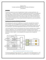
Application Note Synchronization and MIMO ... - Ettus Research
Application Note Synchronization and MIMO ... - Ettus Research
Application Note Synchronization and MIMO ... - Ettus Research

Create successful ePaper yourself
Turn your PDF publications into a flip-book with our unique Google optimized e-Paper software.
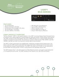
<strong>Application</strong> <strong>Note</strong><br />
<strong>Synchronization</strong> <strong>and</strong> <strong>MIMO</strong> Capability with USRP Devices<br />
<strong>Ettus</strong> <strong>Research</strong><br />
Introduction<br />
Some applications require synchronization between multiple USRP (Universal Software Radio<br />
Peripheral) devices. To meet these requirements, the <strong>Ettus</strong> <strong>Research</strong> USRP N200 <strong>and</strong> USRP N210<br />
kits provide a <strong>MIMO</strong> cable that allows the user to easily build a 2X2 system. External 10 MHz <strong>and</strong> 1<br />
PPS signals can also be used to synchronize all <strong>Ettus</strong> <strong>Research</strong> USRP models, except for the USRP1.<br />
Some USRP models provide the option to integrate an internal GPS Disciplined Oscillator, which<br />
enables timing synchronization over wider geographic areas. This document will introduce <strong>and</strong> explain<br />
the synchronization features of the Universal Software Radio Peripheral (USRP) product family.<br />
<strong>MIMO</strong> Requirements – Time <strong>and</strong> Frequency <strong>Synchronization</strong><br />
For a transceiver to be considered <strong>MIMO</strong> capable, each channel in the radio must meet two<br />
requirements:<br />
1. The sample clocks must be synchronized.<br />
2. The sample times must be aligned when any DSP operations occur.<br />
The <strong>Ettus</strong> <strong>Research</strong> USRP N200/N210 <strong>and</strong> USRP1 meet both of these requirements. In the case of the<br />
USRP N200/N210, this is achieved by sharing a common 10 MHz reference <strong>and</strong> 1 PPS signal to two or<br />
more devices. A <strong>MIMO</strong> system can be built with the USRP N200/N210 <strong>MIMO</strong> cable, or by using an<br />
external reference. The USRP1 contains slots for two daughterboards, <strong>and</strong> uses a common clock<br />
source for all operations. 10 MHz reference <strong>and</strong> 1 PPS inputs are not provided on the USRP1, but are<br />
not required for <strong>MIMO</strong> operation since the USRP1 has two daughterboard slots.<br />
Beamforming <strong>and</strong> Direction Finding Requirements<br />
Some <strong>MIMO</strong> systems are not ideal for applications requiring beamforming or direction finding (DF)<br />
capability. These application areas require a prior knowledge of the phase relationships between<br />
multiple channels. Due to phase ambiguities caused by phased-locked loops, it is possible a software<br />
defined radio (SDR) can have sample clock <strong>and</strong> time alignment, but not phase alignment. In this<br />
context, phase alignment implies a minimal difference between multiple transmit/receive channels, or<br />
that the phase differences can be measured <strong>and</strong> compensated for.<br />
Other Variables That Effect Phase Alignment<br />
As mentioned, other variables aside from LO phase offsets contribute to channel-to-channel phase<br />
error. Filters, mixers, amplifiers <strong>and</strong> other components produce phase variations that vary with time,<br />
temperature, mechanical conditions, etc. These types of errors can generally be calibrated out with<br />
intermittent, low-rate routines detecting the channel-to-channel phase with a common signal generator.<br />
These errors will not change with each PLL retune but may change over time <strong>and</strong> temperature<br />
variation.
<strong>MIMO</strong> Capability vs. Phase Alignment<br />
While applications such as direction finding <strong>and</strong> beamforming require knowledge of the phase offsets<br />
between channels, many <strong>MIMO</strong> implementations do not require a prior knowledge of the phase<br />
relationships between channels. In these cases, the phase differences between channels can be<br />
measured with a training sequence during a frame preamble. Many wireless devices, such as WiFi,<br />
routers work on this concept. <strong>Application</strong>s such as direction finding or adaptive beamforming do<br />
require a prior knowledge of the phase relationships between channels. In these cases, a combination of<br />
the resynchronization methods described above <strong>and</strong> calibration can be used to derive these<br />
relationships.<br />
USRP B100 <strong>and</strong> E100 <strong>Synchronization</strong> – Not <strong>MIMO</strong> Capable<br />
Like the USRP N200/N210, the USRP B100 <strong>and</strong> E100/110 can be synchronized with an external<br />
reference <strong>and</strong> PPS source. However, note this does not imply the USRP B100 <strong>and</strong> E100/E110 are<br />
<strong>MIMO</strong> capable in all cases. The flexible frequency clocking architecture used in the USRP B100 <strong>and</strong><br />
E100/110 produces phase ambiguity in ADC/DAC sample clock. Therefore, sample edges are no<br />
longer aligned <strong>and</strong> the requirements for <strong>MIMO</strong> are not met.<br />
Despite the sample edge misalignment, it is still possible to produce samples with accurate time stamps<br />
for each sample. This is useful for time-difference-of-arrival or similar algorithms.<br />
One exception to these statements is when you make use of a daughterboard containing more than one<br />
channel in a single slot. For example, LFRX/TX, BasicRX/TX, <strong>and</strong> TVRX2 can all be used to achieve<br />
<strong>MIMO</strong> capability with a USRP B100 <strong>and</strong> E100/110. This is because the same clock is used for both<br />
channels.<br />
<strong>Synchronization</strong> with GPS Disciplined Oscillator<br />
It is also possible to provide synchronization over a wider geographic area with a GPS disciplined<br />
oscillator (GPSDO). A GPSDO derives a 10 MHz <strong>and</strong> 1 PPS reference from received GPS signals.<br />
The GPSDO is accurate to approximately +/-50 ns across the globe. <strong>Ettus</strong> <strong>Research</strong> provides an<br />
optional GPSDO module with the USRP N200/N210. An optional GPSDO module can be integrated<br />
into the USRP N200/N210, <strong>and</strong> this module can be purchased from <strong>Ettus</strong> <strong>Research</strong>.<br />
Figure 1 - GPSDO<br />
<strong>MIMO</strong> Capability of <strong>Ettus</strong> <strong>Research</strong> USRP Devices
Table 1 provides an overview of the synchronization <strong>and</strong> <strong>MIMO</strong> capabilities of the USRP product line.<br />
<strong>Note</strong> the USRP B100 <strong>and</strong> E100/110 are not shown as <strong>MIMO</strong> capable. However, some daughterboards<br />
with multiple channels can provide <strong>MIMO</strong> capability in a single slot.<br />
USRP Model<br />
BW Capability<br />
(MSPS w/<br />
16-bit)<br />
System<br />
Clock<br />
Input<br />
<strong>MIMO</strong><br />
Capable<br />
Ext Ref.<br />
Input<br />
1 PPS Input<br />
Internal<br />
GPSDO<br />
Option<br />
Plug <strong>and</strong><br />
Play <strong>MIMO</strong><br />
USRP1 8 X X<br />
N200 25 X X X X X<br />
N210 25 X X X X X<br />
E100 4 X X X<br />
E110 4 X X X<br />
B100 8 X X<br />
Table 1- USRP <strong>Synchronization</strong> Capabilities<br />
In order to provide additional translation between the USRP synchronization mechanisms summarized<br />
summarized in Table 1 <strong>and</strong> the characteristics provided by the daughterboards, Table 2 is presented. In<br />
this matrix, “<strong>MIMO</strong>” means that both time <strong>and</strong> sample clock alignment are possible with multiple<br />
USRP devices. “Time” means samples can be provided with known sample times, while “phase”<br />
means the daughterboard local oscillators can generate a phase aligned LO or, in the case of the Basic<br />
<strong>and</strong> LF boards, there is no local oscillator.<br />
USRP N200/N210 USRP USRP<br />
USRP1<br />
B100 E100/110<br />
SBX <strong>MIMO</strong>, Time, Phase* Time Time <strong>MIMO</strong>, Time<br />
WBX <strong>MIMO</strong>, Time Time Time <strong>MIMO</strong>, Time<br />
XCVR2450 <strong>MIMO</strong>, Time Time Time <strong>MIMO</strong>, Time<br />
DBSRX2 <strong>MIMO</strong>, Time Time Time <strong>MIMO</strong>, Time<br />
TVRX2 <strong>MIMO</strong>, Time Time Time <strong>MIMO</strong>, Time<br />
BasicRx/TX <strong>MIMO</strong>, Time, Phase Time Time <strong>MIMO</strong>, Time,<br />
Phase<br />
LFRX/LFTX <strong>MIMO</strong>, Time, Phase Time Time <strong>MIMO</strong>, Time,<br />
Phase<br />
Table 2 - <strong>Synchronization</strong> Capability vs. Daughterboard <strong>and</strong> USRP<br />
Table 3 shows options for assembling <strong>MIMO</strong> systems of various sizes with a USRP device. When<br />
“external” is stated, you should synchronize multiple devices, or pairs of devices, with a distributed<br />
copy of a 10 MHz <strong>and</strong> 1 PPS signal. This is accomplished with passive or active splitters. This<br />
implementation is discussed in more detail in latter sections.<br />
USRP Model 2x2 <strong>MIMO</strong> 4x4 <strong>MIMO</strong> M x N <strong>MIMO</strong><br />
USRP1 2x Daughterboard Not Recommended Not Recommended<br />
N200/N210 <strong>MIMO</strong> Cable <strong>MIMO</strong> Cable + External External<br />
Table 3- <strong>MIMO</strong> Implementation Options
N200/N210 – Plug <strong>and</strong> Play 2x2 <strong>MIMO</strong> System<br />
The easiest method to implement a high-performance 2x2 <strong>MIMO</strong> system is to utilize two N200/N210s<br />
synchronized with a single <strong>MIMO</strong> cable. In this configuration, a single Gigabit Ethernet (GigE)<br />
interface is used to access both USRP devices. The USRP connected to the GigE acts as a switch <strong>and</strong><br />
provide data/to from both USRP devices. It will also h<strong>and</strong>le time synchronization of the data so the<br />
synchronization process is transparent.<br />
Consider the throughput capability of the N200/N210s GigE interface in this example. The total<br />
sample rate for USRP devices connected to a single GigE port on the host computer cannot exceed 25<br />
MS/s in 16-bit mode, or 50 MS/s in 8-bit mode.<br />
The UHD API allows you to select synchronization settings. These settings are exposed to the GNU<br />
Radio Companion (GRC) blocks. This allows for a quick, illustrative example of how to use the<br />
N200/N210 <strong>MIMO</strong> system. GRC is used for the basic illustration of the N200/N210s <strong>MIMO</strong><br />
capability.<br />
Figure 2 shows a system receiving data from two unsynchronized USRP devices accessed via two<br />
separate GigE interfaces via external switch. The flowgraph reads the streams from the independent<br />
UHD sources, <strong>and</strong> plots the real component on a single scope. A 400.01 MHz signal is injected into<br />
both USRP devices, <strong>and</strong> the real component in shown on a WX GUI Scope. Under ideal conditions,<br />
this yields a constant 10 kHz tone on both channels. Notice in Figure 3 there are obvious phase <strong>and</strong><br />
frequency differences between the two signals. This is a result of variations in the two unsynchronized<br />
reference clocks. The frequency difference is caused primarily between differences in the<br />
daughterboard LO. Heat is applied to one of the USRP devices to accentuate the frequency variation<br />
between the two units.<br />
Figure 2- GRC - Un-Synchronized Reception with Two USRP N200/210s
Figure 3- Phase <strong>and</strong> Frequency Differences in Time Domain Display w/ Asynchronous USRP devices<br />
The plug <strong>and</strong> play 2X2 system is illustrated in the block diagram below. Notice the relative simplicity<br />
of the system. A <strong>MIMO</strong> system is created simply by connecting two N200/N210s with a <strong>MIMO</strong> cable<br />
sharing both the Ethernet connectivity <strong>and</strong> a single 10 MHz reference. A signal generator drives the<br />
receive inputs of both inputs via a two-way splitter to assist with a demonstration of this system. A<br />
flowgraph showing the GNU Radio connectivity is shown in Figure 5.<br />
RF Signal Generator<br />
2-Way Splitter<br />
USRP N210<br />
<strong>MIMO</strong><br />
Cable<br />
USRP N210<br />
1x<br />
GigE<br />
Host PC<br />
Figure 4 - N200/N210 2x2 Reference Design <strong>and</strong> Test
Figure 5 - GRC Flowgraph of w/ 2X2 <strong>MIMO</strong> System<br />
A single UHD block is used in the GRC flowgraph. The block parameters are configured to set up a<br />
2x2 <strong>MIMO</strong> system. The settings of interest are:<br />
Device addr: addr0=192.168.10.2,addr1=192.168.10.3<br />
Sync = don't sync<br />
Num Mboards = 2<br />
Mb0 Clk Src = Default<br />
Mb0 Time Src = Default<br />
…<br />
Mb1 Clk Src = <strong>MIMO</strong> Cable<br />
Mb1 Time Src = <strong>MIMO</strong> Cable<br />
These settings configure the first USRP device, Mb0, which is the first device occurring in the address<br />
string to use its default reference for clocking <strong>and</strong> timing. The second USRP (Mb1) is configured to<br />
accept its frequency <strong>and</strong> timing reference from the <strong>MIMO</strong> cable. The signals are provided by Mb0.<br />
All other st<strong>and</strong>ard settings such as center frequency <strong>and</strong> gain assignments apply as well.<br />
Like the first flowgraph shown, the real part of each USRP channel is displayed on a scope. A phase<br />
correction hier block is included to compensate for the r<strong>and</strong>om, but constant, phase offset discussed<br />
earlier in this paper. A reference signal of 400.010 MHz is injected into both USRP devices through a<br />
splitter <strong>and</strong> cables equal length. Figure 6 includes a screenshot of the resultant display both before<br />
phase adjustment. <strong>Note</strong> the phase is constant <strong>and</strong> can be easily tuned by h<strong>and</strong> with the flowgraph<br />
shown.
Figure 6- Time Domain Display Showing Received Signal before Phase Compensation<br />
Figure 7 shows signals from the two synchronized N210s with phase correction applied. In this plot, it<br />
is clear the <strong>MIMO</strong> connection has enabled the frequency <strong>and</strong> time references to be synchronized. The<br />
r<strong>and</strong>om, but constant, phase offset discussed above is corrected with a complex phase shift in the<br />
flowgraph. In real applications, this phase correction would be implicitly generated with algorithms<br />
such as MRC, or periodic calibration.<br />
Figure 7- Time Domain Display Showing Received Signal with Phase Compensation<br />
This is a simple illustration of the <strong>MIMO</strong> capability provided by the USRP N200/N210. Keep in mind<br />
in most applications the phase compensation is implemented with some automated process. However,
calibrating the devices with this type of manual correction <strong>and</strong> a calibration source is certainly an<br />
option. All principles here apply equally to operations in the transmit direction.<br />
Larger <strong>MIMO</strong> Systems<br />
Utilizing the external reference <strong>and</strong> 1 PPS inputs, it is possible to build a system larger than 2X2 with<br />
an N200/N210. It is possible to reduce the overall cost of a system by utilizing the plug <strong>and</strong> play<br />
<strong>MIMO</strong> capability to create pairs of USRP devices. For example, if you want to build a 4X4 <strong>MIMO</strong><br />
system, two sets of N200/N210 pairs can be used. A distribution amplifier can be used to split a<br />
common 10 MHz reference <strong>and</strong> 1 PPS signal. An illustration of this setup is shown in Figure 8.<br />
USRP N200<br />
<strong>MIMO</strong><br />
Cable<br />
USRP N200<br />
USRP N200<br />
<strong>MIMO</strong><br />
Cable<br />
USRP N200<br />
Splitter<br />
Splitter<br />
1x GigE<br />
1x GigE<br />
10 MHz<br />
Clock<br />
Source<br />
1 PPS<br />
Source<br />
Gigabit<br />
Ethernet<br />
Switch<br />
Host PC<br />
Figure 8- 4X4 <strong>MIMO</strong> Configuration<br />
In this case, a pair of signal splitters/amplifiers is used to distribute the reference <strong>and</strong> 1 PPS signals to<br />
two pairs of N200/N210s. In this testing, <strong>Ettus</strong> <strong>Research</strong> used the TADD series from TAPR, which is<br />
no longer produced <strong>and</strong> not universally compatible to USRP devices other than the N200/N210.<br />
Alternative options are presented later in this document. A low-cost alternative can use a passive RF<br />
splitter for the 10 MHz reference <strong>and</strong> 74AC series logic for the 1 PPS signal. A GigE switch is used to<br />
communicate with the two pairs of N200/N210s. The constraints of GigE effectively limit the total<br />
sample b<strong>and</strong>width to 25 MSPS in each direction when 16-bit samples are used. This translates to 6.25
MSPS or less per channel. <strong>Ettus</strong> <strong>Research</strong> has had success using the EXPI9404PTLBLK 4-Port GigE<br />
card to provide full-rate access to four USRP device simultaneously.<br />
Figure 9 - <strong>Ettus</strong> <strong>Research</strong> 4X4 Reference Design<br />
External Distribution Options <strong>and</strong> Other <strong>Note</strong>s<br />
There are several options to provide the external distribution required for large <strong>MIMO</strong> system. The<br />
quality of the distribution component will determine the cost, <strong>and</strong> ultimately the performance, of the<br />
synchronization. The performance parameters of interest are peak-to-peak timing error, <strong>and</strong> or/ phase<br />
noise in the case of the frequency reference. <strong>Note</strong> all cables from the external distribution devices<br />
should connected to their respective USRP devices with matched length cable of the same type <strong>and</strong><br />
connectorization.<br />
Possible distribution devices can be seen in Table 4. Other devices can be used, but care should be<br />
taken to meet the input requirements for the associated USRP radio. These requirements are seen in<br />
Table 5. Remember any time a signal pass through a two-way splitter the resultant signals are -3 dB<br />
relative to the original reference.
1 PPS Distribution* Clock Distribution*<br />
Passive 2-Way RF Splitter<br />
Part: ZFSC-2-1W<br />
Cost: ~$50<br />
Manufacturer: Mini-Circuits<br />
74 Series TTL/CMOS<br />
Part: 74AC04<br />
Cost: < $5<br />
Manufacturer: n/a<br />
1:4 TTL Fanout Buffer<br />
Part: PRL-414B<br />
Cost: $415<br />
Manufacturer: Pulse <strong>Research</strong><br />
Active, 4-Way 10 MHz Splitter<br />
Part: DEM 10-4<br />
Cost: $75 (assembled w/ enclosure)<br />
Manufacturer: Down East Microwave<br />
Table 4 – Potential Clock <strong>and</strong> PPS Distribution Options<br />
*Solutions not warranted by <strong>Ettus</strong> <strong>Research</strong>. Final selection must be based on users requirements.<br />
USRP Model 1 PPS Specification External Ref. Specification*<br />
N200 3.3-5V 0 to 18dBm<br />
N210 3.3-5V 0 to 18dBm<br />
USRP2 5V 5 to 18dBm<br />
E100 3.3-5V 5 to 15 dBm<br />
E110 3.3-5V 5 to 15 dBm<br />
B100 3.3-5V 5 to 15 dBm<br />
USRP1 – Low-Cost 2X2 <strong>MIMO</strong> System<br />
Table 5- External Reference <strong>and</strong> 1PPS Input Specifications<br />
*50 ohm Terminated<br />
It is possible to use the USRP1 as a 2X1 <strong>MIMO</strong> transceiver in applications requiring a more costsensitive<br />
solution. The USRP1 contains two receive DSP chains <strong>and</strong> one transmit DSP chain. The<br />
aggregate host b<strong>and</strong>width of the USRP1 is 8 MS/s in 16-bit mode. This limits the practical use of a full<br />
duplex, symmetric, 2x1 <strong>MIMO</strong> transceiver to 2 MHz of usable b<strong>and</strong>width per channel. The GRC<br />
flowgraph in Figure 10 shows how the USRP1 can be accessed in a <strong>MIMO</strong> configuration. The key<br />
parameters that need correct settings are:<br />
Num Mboards: 1<br />
Num Channels: 2<br />
Clock Source: Default<br />
Mb0: Subdev Spec: A:0 B:0<br />
The Subdev Spec must contain enough terms to specify the input for each channel. As you access two<br />
channels, you must include to Subdec Spec terms, “A:0” <strong>and</strong> “B:0.”. This specifies the receive<br />
connection of each of the SBXs used in this particular setup.
Figure 10 - Two Channel <strong>MIMO</strong> Flowgraph with USRP1<br />
While the USRP1 does provide <strong>MIMO</strong> capability, it does not have an external reference or 1 PPS input.<br />
Thus, it cannot be easily exp<strong>and</strong>ed to a system larger than 2X2. If a system larger than 2X2, or more<br />
than 2 MHz of b<strong>and</strong>width per channel is required, the N200/N210 is the recommended solution.<br />
Conclusion<br />
This application note discusses some of the basic principles associated with <strong>MIMO</strong> system<br />
implementation using an <strong>Ettus</strong> <strong>Research</strong> USRP SDR. GRC flowgraphs are used for a conceptual<br />
demonstration of phase coherency versus phase alignment capabilities. Reference designs for 2X2 <strong>and</strong><br />
4X4 systems, <strong>and</strong> potential distribution elements, are shown. Additional information on how to use the<br />
UHD API to manage synchronization in software can be found at:<br />
http://files.ettus.com/uhd_docs/manual/html/sync.html<br />
We invite <strong>and</strong> appreciate your feedback, which can be provided to support@ettus.com<br />
References<br />
Mini-Circuits. (n.d.). Mini-Circuits. Retrieved February 15, 2012, from http://www.minicircuits.com/