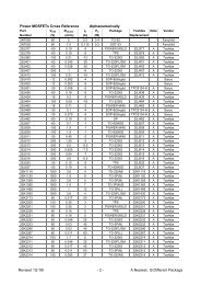
Stag PP39 Users Manual - Matthieu Benoit
Stag PP39 Users Manual - Matthieu Benoit
Stag PP39 Users Manual - Matthieu Benoit

Create successful ePaper yourself
Turn your PDF publications into a flip-book with our unique Google optimized e-Paper software.
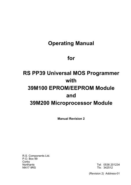
Operating <strong>Manual</strong><br />
for<br />
RS <strong>PP39</strong> Universal MOS Programmer<br />
with<br />
39M100 EPROM/EEPROM Module<br />
and<br />
39M200 Microprocessor Module<br />
<strong>Manual</strong> Revision 2<br />
R.S. Components Ltd.<br />
P.O. Box 99<br />
Corby<br />
Northants<br />
NN17 9RS<br />
Tel: 0536 201234<br />
Tlx: 342512<br />
(Revision 2) Address-01
RS <strong>PP39</strong> CONTENTS<br />
Section 1 GENERAL INTRODUCTION<br />
1.1 Introduction<br />
1.2 Modules<br />
1.3 The Keyboard<br />
1.4 Initial Setting-up Procedure<br />
1.5 Selection of Local and Remote Modes<br />
39M100<br />
Section 2 39M100 INTRODUCTION<br />
2.1 The 39M100 Module<br />
2.2 RAM Operating Structure<br />
2.3 List of ‘Set’ Commands<br />
Section 3 SELECTING A DEVICE<br />
3.1 Selecting a Device<br />
3.2 List of Devices and Device Codes<br />
3.3 Electronic Identifier<br />
Section 4 BIT MODE<br />
4.1 Selection of Bit Mode Configuration<br />
4.2 8-Bit Mode<br />
4.3 Gang Mode<br />
4.4 16-Bit Mode<br />
4.5 32-Bit Mode<br />
Section 5 DEVICE FUNCTIONS<br />
5.1 Load<br />
5.2 Empty Test<br />
5.3 Pre-Program Bit Test<br />
5.4 Programming<br />
5.5 Verify<br />
5.6 Access Time Testing<br />
5.7 Checksum and Cyclic Redundancy Check (CRC)<br />
5.8 Device/RAM Address Limits<br />
5.9 Save and Recall Machine Configurations<br />
Section 6 RAM FUNCTIONS<br />
6.1 Interlace *<br />
6.2 List and Edit<br />
6.3 Insert<br />
6.4 Delete<br />
6.5 Block Move<br />
6.6 Filling the RAM<br />
6.7 String Search<br />
(Revision 2) Contents-01
39M200<br />
Section 7 39M200 INTRODUCTION<br />
7.1 39M200 Module<br />
7.2 RAM operating structure<br />
7.3 List of ‘SET’ Commands<br />
Section 8 SELECTING A DEVICE<br />
8.1 Device Type Selection<br />
8.2 List of Devices and Device Codes<br />
Section 9 DEVICE FUNCTIONS<br />
9.1 Load<br />
9.2 Empty Test<br />
9.3 Programming<br />
9.3.1 Verify Pass-Security Bit<br />
9.3.2 In-program Verify<br />
9.4 Checksum<br />
9.5 Device/RAM address limits<br />
9.6 Save and Recall Machine Configurations<br />
9.7 68705 Device<br />
Section 10 RAM FUNCTIONS<br />
10.1 List<br />
10.2 Edit<br />
10.3 Insert<br />
10.4 Delete<br />
10.5 Block move<br />
10.6 Filling the RAM<br />
10.7 String Search<br />
39M100 and 39M200<br />
Section 11 INTERFACE<br />
11.1 Setting the Input/Output Interface Parameters<br />
11.2 Input/Output Operations<br />
11.2.1 Input Parameters<br />
11.2.2 Output Parameters<br />
11.3 Error Reporting on Input/Output<br />
Section 12 FORMAT DESCRIPTIONS<br />
12.1 Interface Formats<br />
12.1.1 Intellec<br />
12.1.2 Extended Intellec<br />
12.1.3 Hex ASCII<br />
12.1.4 Exorcisor<br />
12.1.5 Extended Exorcisor<br />
12.1.6 Tek-Hex<br />
12.1.7 Extended Tek-Hex<br />
12.1.8 PPX or <strong>Stag</strong> Hex<br />
12.1.9 Binary, DEC Binary and Binary Rubout<br />
Contents-02
Section 13 RS232C HARDWARE DESCRIPTIONS<br />
13.1 RS232C Interface Port Connections<br />
13.2 XON/XOFF (3 wire cable form)<br />
13.3 Hardware Handshake (7 or 8 wire cable form)<br />
13.4 Non-Standard Connections<br />
Section 14 REMOTE CONTROL<br />
14.1 Selecting Remote Control<br />
14.2 Remote Control Commands<br />
14.3 Remote Error Words and Codes<br />
Section 15 SPECIFICATION<br />
15.1 The ASCII code<br />
15.2 Specification<br />
(Revision 2) Contents-03
SECTION 1
1.–GENERAL INTRODUCTION
1.1 INTRODUCTION<br />
The <strong>PP39</strong> is a Universal MOS Programmer, which in conjunction with its<br />
family of modules is capable of supporting all MOS erasable PROM and<br />
MICRO devices in NMOS and CMOS technology.<br />
The Programmer is software controlled using a single level module<br />
approach. This ensures flexibility and ease of upgrade for future devices;<br />
whereby the module alone can be returned for software upgrades. (For<br />
urgent programming needs a module exchange plan is available).<br />
The <strong>PP39</strong> can be operated in ‘LOCAL’ mode or it can be linked to a<br />
computer via the serial RS232C interface port enabling ‘REMOTE’ operation<br />
of the machine.<br />
RS <strong>PP39</strong> MAINFRAME<br />
Two polarised sockets provide<br />
interconnections from the main frame to the<br />
<strong>PP39</strong> modules.<br />
Four locating pins<br />
provide automatic module<br />
alignment.<br />
Keyboard: For data entry and<br />
operating programmer<br />
functions.<br />
16-Character<br />
Green alphanumeric display<br />
(Revision 2) 1.1-01
39M 100 EPROM & EEPROM MODULE<br />
SPECIFICATIONS<br />
FUSES<br />
POWER<br />
CONNECTION<br />
SERIAL RS232C<br />
INTERFACE<br />
PORT CONNECTOR<br />
MAINS POWER<br />
ON/OFF SWITCH<br />
1.1-02
1.2 MODULES<br />
A variety of modules is available to plug into the main frame. This<br />
guarantees future flexibility to support new devices as they are<br />
developed.<br />
39M100 – EPROM/EEPROM<br />
This module supports NMOS and CMOS, EPROM and EEPROM devices in<br />
both 24 and 28 pin DIPs packages. The module features algorithms for fast<br />
programming and it supports Silicon Signature* technology for automatic<br />
device identification. Sockets are provided for set programming of two<br />
devices simultaneously or they can be used as a mini-ganger. The <strong>PP39</strong><br />
can be configured as an 8, 16 or 32 bit machine. Access time tests can be<br />
performed and an auto-recall feature is incorporated where pre-set<br />
parameters can be recalled from a non-volatile memory at any time for ease<br />
of use.<br />
39M200 MICROPROCESSOR MODULE<br />
This module will program single chip microprocessors containing EPROM<br />
from AMD, Intel, NEC and Motorola in both 40 pin and 28 pin DIPs<br />
packages.<br />
(Revision 2) 1.2-01
1.2-02
1.3 THE KEYBOARD<br />
For data entry and operating programmer functions<br />
load<br />
7 8 9 E F<br />
input<br />
output<br />
TO LOAD A MASTER DEVICE OR DEVICES<br />
TO EXECUTE AN INPUT VIA THE RS232C<br />
INTERFACE PORT<br />
4 5 6 C D<br />
1 2 3 A B<br />
HEXADECIMAL KEY<br />
TO ENTER DATA<br />
OR TO SELECT<br />
PARAMETERS<br />
AND SPECIAL<br />
FUNCTIONS<br />
TO EXECUTE AN OUTPUT VIA THE RS232C<br />
INTERFACE PORT<br />
0 ↑ ↓ ← →<br />
edit<br />
list<br />
TO MODIFY THE RAM DATA<br />
CURSOR KEYS – TO MANIPULATE<br />
DATA OR TO MOVE PARAMETERS ON<br />
THE DISPLAY FOR EASE OF USE.<br />
TO SET AN ADDRESS AND DISPLAY THE<br />
DATA IN THAT LOCATION<br />
set<br />
verify<br />
TO SET FUNCTIONS OR PARAMETERS INTO<br />
THE PROGRAMMER<br />
TO EXECUTE DEVICE VERIFICATION WITH<br />
SPECIAL ADDRESS LIMITS<br />
c/sum<br />
TO PERFORM A CHECKSUM OF THE RAM<br />
WITHIN THE DEVICE ADDRESS RANGE<br />
SPECIFIED<br />
empty<br />
TO EXECUTE AN EMPTY CHECK WITHIN<br />
SPECIFIED ADDRESS LIMITS<br />
exit<br />
program<br />
TO EXIT FROM A MODE OR FUNCTION<br />
TO EXECUTE A PROGRAMMING SEQUENCE<br />
WITH PRE-SET PARAMETERS FOR TEST<br />
OPTIONAL FEATURES<br />
RAM EXTENSION BOARD<br />
The <strong>PP39</strong> is presently supplied as standard with 512K bits of RAM. As<br />
larger devices become available this will prove to be inadequate and more<br />
RAM will be required.<br />
Therefore the <strong>PP39</strong> has the facility to have its RAM expanded to 1M-bits,<br />
2M-bits, 4M-bits and beyond.<br />
(Revision 2) 1.3-01
1.3-02
1.4 INITIAL SETTING UP PROCEDURE<br />
Before attempting to apply power to your <strong>PP39</strong> Programmer ensure that<br />
it is set to the correct operating voltage for your power source. The<br />
voltage setting is printed on the rear panel.<br />
1. Plug the supplied Power cord into the rear panel socket<br />
2. Apply power to the machine from the mains power source<br />
3. Power-up the machine using the ON/OFF switch on the rear panel<br />
After “POWER UP” and without a 39-Module inserted the display will<br />
read:<br />
MODULE ?<br />
The mainframe software revision can now be ascertained prior to the<br />
module being inserted simply by pressing the key marked ‘SET’ followed<br />
by the key marked ‘6’, e.g.<br />
<strong>PP39</strong> ISS 04<br />
to remove press ‘EXIT’<br />
In order to make this manual as straightforward as possible the action of<br />
pressing the key marked ‘SET’ followed by another key or keys will be<br />
abbreviated to a single instruction e.g. ‘SET 6’, ‘SET F3’, ‘SET INPUT’ etc.<br />
Note<br />
To ensure correct initialisation, power down before inserting a module.<br />
Always wait five seconds before applying power again.<br />
(Revision 2) 1.4-01
INTRODUCTION OF A 39-MODULE TO THE MAIN FRAME<br />
Having completed the setting up procedure the <strong>PP39</strong> is ready to receive<br />
its 39-Module. Controlling software for the machine resides in the<br />
selected module, therefore the operation of the Programmer is dependent<br />
upon the type of 39-Module plugged into the main frame.<br />
On power-up the programmer will be configured automatically to what it<br />
was before the machine was last powered down.<br />
This ensures that once any machine parameter has been set-up, it needn’t<br />
be reset every time the machine is switched on.<br />
For instance, if the machine was previously used in the ‘LOCAL’ mode<br />
with the 39M100 Eprom Module inserted, the initial configuration of the<br />
machine will be set on power-up and the display will show the last<br />
entered manufacturer, device type and selected mode, such as:<br />
AMD 2764<br />
GANG<br />
To determine the software revision of the Module press ‘SET 6’ and the<br />
display will show:<br />
MODULE M100 07<br />
To remove, press ‘EXIT’.<br />
1.4-02
1.5 SELECTION OF ‘LOCAL’ OR ‘REMOTE’ MODES<br />
The Programmer will be in either ‘Local’ or ‘Remote’ on power up.<br />
To Select Local Mode<br />
When the machine is in remote mode on power-up the display will show<br />
manufacturer, device type and remote mode itself. For instance:<br />
Manufacturer Device type Remote mode<br />
SEQ 5516A REM<br />
To exit from remote one of two sequences can be performed:<br />
(i) If the programmer is connected via the I/O port to a computer or<br />
terminal keyboard then the sequence of pressing Key ‘Z’ followed<br />
by Key ‘RETURN’ will bring control back to ‘local’ on the <strong>PP39</strong><br />
keyboard.<br />
(ii) If the <strong>PP39</strong> is in stand alone mode on power-up but, still under the<br />
‘remote’ setting, the operator must power down wait five seconds and<br />
then power up again with the ‘EXIT’ key depressed to reach<br />
‘local’ mode.<br />
When either sequence (i) or (ii) is performed the display will show<br />
manufacturer, device type and bit mode for instance a typical ‘local’<br />
mode setting for the 39M100 might be:<br />
Manufacturer Device type Bit mode<br />
SEQ 5516A M8<br />
In local mode all functions of the <strong>PP39</strong> are controlled from its own<br />
keyboard.<br />
(Revision 2) 1.5-01
REMOTE CONTROL<br />
To select remote control<br />
Press set 2 and the display will show:<br />
REMOTE PRESS SET<br />
By pressing set again, the display will show the manufacturer, device type<br />
and remote mode.<br />
For instance:<br />
Manufacturer Device type Remote mode<br />
SEQ 5516A REM<br />
In the remote mode, the <strong>PP39</strong> operates under remote control from a<br />
computer or a terminal. The keyboard of the <strong>PP39</strong> is inoperative at this<br />
time and the display will only show information as requested under remote<br />
control.<br />
1.5-02
SECTION 2
39M100
(Revision 2) 2.1-01
2.1-02
2.2 RAM OPERATING STRUCTURE<br />
(Revision 2) 2.2-01
2.2-02
2.3 LIST OF ‘SET’ COMMANDS<br />
set 0<br />
set 1<br />
set 2<br />
set 3<br />
Allows user to scan and select various manufacturers<br />
and device types<br />
Selects interface parameters<br />
Format, Baud Rate, Word Length, Stop Bits, Parity<br />
Sets programmer into ‘Remote’ control. (To return<br />
to Local Mode: Power up with exit key depressed)<br />
Selects mode of machine, i.e. 8-Bit, 16-Bit, 32-Bit<br />
or GANG operating mode.<br />
set 4<br />
Displays RAM size in hexadecimal<br />
set 5<br />
RAM data complemented from lower to upper address limit<br />
set 6<br />
Displays module software revision if module is plugged in,<br />
or main frame software revision, if no module is plugged in.<br />
set 7<br />
Verifies device under access time control<br />
set 8<br />
Calculates and displays CRC (Cyclic Redundancy Check)<br />
set A1<br />
To<br />
A9<br />
Saves machine configuration<br />
(up to nine sets)<br />
(Revision 2) 2.3-01
LIST OF ‘SET’ COMMANDS (continued)<br />
set B1<br />
set F0<br />
To<br />
B9<br />
Recalls previously saved machine<br />
configurations (up to 9 sets)<br />
Fills entire RAM with 00<br />
set FF<br />
Fills entire RAM with FF<br />
set F1<br />
set F2<br />
set F4<br />
set F6<br />
set F7<br />
Audible Alarm: To indicate end of program, test, or<br />
as a warning using a combination of bleeps and tones.<br />
SET F1 both enables and disables this function.<br />
Fills RAM with arbitrary variable from lower to upper<br />
address limit<br />
Block Move: A block of data with pre-selected<br />
address limits can be copied and then re-located at<br />
another address within the RAM.<br />
Defines RAM and device address ranges for all functions<br />
which operate on the device<br />
Access time calibration – Provides repetitive waveform<br />
for access time calibration<br />
set input<br />
Input – Enters input address offset<br />
set output<br />
Output – Enters output address offset, start address<br />
and stop address<br />
2.3-02
LIST OF ‘SET’ COMMANDS (continued)<br />
set E1<br />
Electronic Identifier: Mode (i) Two Key Operation<br />
set E2<br />
Electronic Identifier: Mode (ii) Single Key Operation<br />
set 9<br />
String Search<br />
set FE<br />
Applicable to MOTOROLA 2816 ONLY – Erases Device<br />
(Revision 2) 2.3-03
2.3-04
SECTION 3
3.1 SELECTING A DEVICE<br />
Selecting the device using a 4 digit code<br />
The complete range of devices supported by the 39M100 is stored<br />
in the module. Each individual device has its own four digit code.<br />
(See device code list Section 3.2)<br />
SET 0 – Allows code selection<br />
SEQUENCE: Prior to SET ‘0’ the display will show the last entered<br />
configuration<br />
For example:<br />
AMD 2716<br />
M8<br />
By pressing SET ‘0’ the device code of this configuration will be displayed:<br />
DEVICE CODE 9F42<br />
When the new device code to be entered is already known. (For instance<br />
AF44 is the code for a Fujitsu 2732 EPROM device.) Then the AF44 can be<br />
entered directly onto the display from the keyboard replacing the old code:<br />
DEVICE CODE AF44<br />
The selection sequence can be completed by pressing EXIT whereby the<br />
new manufacturer and device type are displayed along with the bit mode:<br />
FUJ 2732<br />
M8<br />
(Revision 2) 3.1-01
Scanning device types and manufacturers by use of cursor keys<br />
When a device code is not known or if the user wishes to scan the devices<br />
available, selection can be made via the cursor keys:<br />
↓ ↑ ← →<br />
By pressing SET ‘0’ the code of the last used device is displayed:<br />
DEVICE CODE AF44<br />
The manufacturer and device type can be changed by use of the cursor<br />
keys:<br />
The up/down keys scan the range of manufacturers.<br />
↓<br />
↑<br />
changes manufacturer<br />
The left/right keys scan the device range of a particular manufacturer.<br />
←<br />
→<br />
changes device type<br />
3.1-02
3.2 LIST OF DEVICES AND DEVICE CODES<br />
This list of parts is supported by the 39M100 Module. Each device<br />
carries a four digit code. The first two digits define the manufacturer of<br />
the device and the second two digits refer to the device type.<br />
EPROMS<br />
Manufacturer Device Device Code Device Size (Hex)<br />
AMD 2716 9F 42 800<br />
2732 9F 44 1000<br />
2732A 9F C4 1000<br />
2764 9F 4A 2000<br />
2764A 9F CA 2000<br />
27128 9F 4B 4000<br />
27128A 9F CB 4000<br />
27256 9F 4C 8000<br />
27512 9F 4D 10000<br />
Fujitsu 2716 AF 42 800<br />
2732 AF 44 1000<br />
2732A AF C4 1000<br />
2764 AF 4A 2000<br />
27128 AF 4B 4000<br />
27256 AF 4C 8000<br />
27C256 AF DC 8000<br />
27C128 AF DB 4000<br />
27C256A AF CC 8000<br />
27C512 AF DD 10000<br />
General 27C64 02 DA 2000<br />
Instruments 27HC64 02 DA 2000<br />
27256 02 4C 8000<br />
27C256 02 DC 8000<br />
Hitachi 2716 BF 42 800<br />
2532 BF 43 1000<br />
2732 BF 44 1000<br />
2732A BF C4 1000<br />
2764 BF 4A 2000<br />
27C64 BF DA 2000<br />
27128 BF 4B 4000<br />
27128A BF CB 4000<br />
27256 BF 4C 8000<br />
27C256 BF DC 8000<br />
27512 BF 4D 10000<br />
(Revision 2+) 3.2-01
LIST OF DEVICES AND DEVICE CODES (continued)<br />
Manufacturer Device Device Code Device Size (Hex)<br />
Intel 2716 6F 42 800<br />
2732 6F 44 1000<br />
2732A 6F C4 1000<br />
2764 6F 4A 2000<br />
2764A 6F CA 2000<br />
27128A 6F CB 4000<br />
27128B 6F CB 4000<br />
27C64 6F DA 2000<br />
27128 6F 4B 4000<br />
27C128 6F DB 4000<br />
27256 6F 4C 8000<br />
27256 ** 6F FC 8000<br />
27C256** 6F DC 8000<br />
27512 6F 4D 10000<br />
27512 ** 6F FD 10000<br />
27513 6F CD 10000<br />
27513 ** 6F FE 10000<br />
87C64 6F EA 2000<br />
87C128 6F EB 4000<br />
87C256 6F EC 8000<br />
Mitsubishi 2716 DF 42 800<br />
2732 DF 44 1000<br />
2732A DF C4 1000<br />
2764 DF 4A 2000<br />
27128 DF 4B 4000<br />
27C128 DF DB 4000<br />
27256 DF 4C 8000<br />
27512 DF 4D 10000<br />
Motorola 2716 7F 42 800<br />
2532 7F 43 1000<br />
2732 7F 44 1000<br />
68764 7F 45 2000<br />
68766 7F 47 2000<br />
National 2716 3F 42 800<br />
2732 3F 44 1000<br />
27C32H 3F 46 1000<br />
27C32B 3F D5 1000<br />
2732A 3F C4 1000<br />
2764 3F 4A 2000<br />
27128 3F 4B 4000<br />
27C16 3F D2 800<br />
27C32 3F D4 1000<br />
27C64 3F DA 2000<br />
27CP128 3F DB 4000<br />
27C256 3F DC 8000<br />
27C512 3F DD 10000<br />
3.2-02
LIST OF DEVICES AND DEVICE CODES (continued)<br />
Manufacturer Device Device Code Device Size (Hex)<br />
NEC 2716 CF 42 800<br />
2732 CF 44 1000<br />
2732A CF C4 1000<br />
2764 CF 4A 2000<br />
27C64 CF DA 2000<br />
27128 CF 4B 4000<br />
27256 CF 4C 8000<br />
27C256 CF DC 8000<br />
27C256A CF CC 8000<br />
27C512 CF DD 10000<br />
Oki 2716 08 42 800<br />
2532 08 43 1000<br />
2732 08 44 1000<br />
2732A 08 C4 1000<br />
2764 08 4A 2000<br />
27128 08 4B 4000<br />
SEEQ 5133 FF 4A 2000<br />
2764 FF 4A 2000<br />
5143 FF 4B 4000<br />
27128 FF 4B 4000<br />
27256 FF 4C 8000<br />
27C256 FF DC 8000<br />
SGS 2716 8F 42 800<br />
2532 8F 43 1000<br />
2732A 8F C4 1000<br />
2764 8F 4A 2000<br />
2764A 8F CA 2000<br />
27128A 8F CB 4000<br />
27256 8F 4C 8000<br />
Signetics 27C64A 1F DA 2000<br />
87C64A 1F EA 2000<br />
SMOS 27C64 0F DA 2000<br />
27128 0F 4B 4000<br />
27C256 0F DC 8000<br />
(Revision 2+) 3.2-03
LIST OF DEVICES AND DEVICE CODES (continued)<br />
Manufacturer Device Device Code Device Size (Hex)<br />
Texas 2516 4F 42 800<br />
Instruments 2532 4F 43 1000<br />
2532A 4F 41 1000<br />
2732A 4F C4 1000<br />
2564 4F 47 2000<br />
2764 4F 4A 2000<br />
27128 4F 4B 4000<br />
27128A 4F CB 4000<br />
27C128 4F DB 4000<br />
27256 4F 4C 8000<br />
27C256 4F DC 8000<br />
27C512 4F DD 10000<br />
Toshiba 2732 EF 44 1000<br />
2732A EF C4 1000<br />
2764 EF 4A 2000<br />
2764A EF CA 2000<br />
27128 EF 4B 4000<br />
27128A EF CB 4000<br />
27256 EF 4C 8000<br />
27256A EF CC 8000<br />
57256 EF DC 8000<br />
VTI 27C64 04 DA 2000<br />
27C128 04 DB 4000<br />
27C256 04 DC 8000<br />
Waferscale 27C64 0B DA 2000<br />
57C64 0B DA 2000<br />
27C128 0B DB 4000<br />
57C49 0B 06<br />
E100 2516 0E 42 800<br />
2716 0E 42 800<br />
2532 0E 43 1000<br />
2732 0E 44 1000<br />
2564 0E 47 2000<br />
2764 0E 4A 2000<br />
87C64 0E EA 2000<br />
27128 0E 4B 4000<br />
87C128 0E EB 4000<br />
27256 0E 4C 8000<br />
87C256 0E EC 8000<br />
27512 0E 4D 10000<br />
** Indicates Quick Pulse Programming Parts<br />
3.2-04
LIST OF DEVICES AND DEVICE CODES (continued)<br />
EEPROMS<br />
Manufacturer Device Device Code Device Size (Hex)<br />
AMD 9864 9F 5A 2000<br />
2817A 9F 58 800<br />
2864B 9F 5C 2000<br />
Exel 2816A 01 52 800<br />
2817A 01 58 800<br />
2864A 01 5C 2000<br />
2865A 01 5C 2000<br />
Hitachi 48016 BF 51 800<br />
58064 BF 5A 2000<br />
58C65 BF 7C 2000<br />
Intel 2816A 6F 52 800<br />
2817 * 6F 53 800<br />
Motorola 2816 7F 52 800<br />
2817 7F 53 800<br />
National 9716 3F 51 800<br />
9817 3F 58 800<br />
98C64 3F 7C 2000<br />
NEC 28C64 CF 7C 2000<br />
Rockwell 2816A 06 52 800<br />
87C32 06 D4 1000<br />
Samsung 2816A 09 52 800<br />
2864A 09 5C 2000<br />
2865A 09 5C 2000<br />
SEEQ 5516A FF 52 800<br />
2816A FF 52 800<br />
5213 FF 53 800<br />
52B13 FF 54 800<br />
52B13H FF 56 800<br />
52B33 FF 5A 2000<br />
52B33H FF 5E 2000<br />
2817A FF 58 800<br />
2864 FF 5B 2000<br />
28C256 FF 7F 8000<br />
28C64 FF 7C 2000<br />
SMOS 2864 0F 5B 2000<br />
(Revision 2+) 3.2-05
LIST OF DEVICES AND DEVICE CODES (continued)<br />
Manufacturer Device Device Code Device Size (Hex)<br />
Xicor X2804A 07 50 400<br />
X2816A 07 52 800<br />
2816H 07 56 800<br />
2816B 07 56 800<br />
28C16 07 76 800<br />
2864A 07 5C 2000<br />
2864B 07 5C 2000<br />
28C64 07 7C 2000<br />
2864H 07 5B 2000<br />
28256 07 5F 8000<br />
28C256 07 7F 8000<br />
* Intel 2817 requires AM100 6F53 Adaptor<br />
3.2-06
3.3 ELECTRONIC IDENTIFIER<br />
Important Node:<br />
Devices which do not contain an Electronic Identifier may be irreparably<br />
damaged if they are used in the Silicon Sig mode.<br />
Electronic Identifier is a term used to describe a code mask programmed<br />
into a PROM which identifies the device type and manufacturer. The code<br />
is stored outside the normal memory array and is accessed by applying 12<br />
Volts to address line A9. This allows the <strong>PP39</strong> to directly identify any<br />
device containing an Electronic Identifier and thus eliminate the need for<br />
the user to select the device type.<br />
The <strong>PP39</strong> presently uses two modes of Silicon Sig operation both of<br />
which only work with 28 pin devices.<br />
Mode (i): Two Key Operation<br />
On pressing SET E1 the display will show “SILICON SIG” alongside the<br />
selected bit-mode:<br />
SILICON SIG M8<br />
If any device function key is pressed e.g. Program, Load etc. the <strong>PP39</strong> will<br />
first attempt to read the signature of any devices present. If no code can<br />
be read or the code is not found in the <strong>PP39</strong>’s list of valid codes the<br />
display will show:<br />
SI SIG NOT FOUND<br />
If two devices are successfully recognised but are incompatible i.e. they<br />
use different programming algorithms the display will show:<br />
UNLIKE DEVICES<br />
If neither of the above two fault conditions occur then the manufacturer<br />
and the device type will be displayed. In the case of devices in both<br />
sockets the manufacturer and device code of the device in the left socket<br />
will be displayed.<br />
To execute the function the specified ‘device function key’ must be pressed<br />
again e.g. Prog, Load etc.<br />
To exit from the Silicon Sig mode select a device using SET 0 in the usual<br />
manner.<br />
(Revision 2) 3.3-01
Mode (ii): Single Key Operation<br />
Pressing SET E2 will again display “SILICON SIG” alongside the selected<br />
bit-mode.<br />
SILICON SIG M8<br />
Operation is similar to the previously described mode except that the <strong>PP39</strong><br />
rather than stopping to display the manufacturer and device type continues<br />
straight on to execute the selected function.<br />
To exit from the Silicon Sig mode select a device using SET 0 in the usual<br />
manner.<br />
3.3-02
SECTION 4
BIT MODES<br />
4.1 SELECTION OF BIT MODE CONFIGURATION<br />
The last used bit mode will already be displayed on power up along with<br />
manufacturer and device type. For instance:<br />
AMD 2764<br />
By pressing SET 3 the bit mode along is shown:<br />
MODE-16 BIT<br />
M16<br />
The range of modes can now be scanned by pressing either the up or<br />
down cursor keys:<br />
MODE-8 BIT<br />
MODE-16 BIT<br />
MODE-32 BIT LO<br />
MODE-32 BIT HI<br />
MODE-GANG<br />
When selection is made press EXIT for operation in chosen mode, e.g.:<br />
AMD 2764<br />
M8<br />
(Revision 2) 4.1-01
4.1-02
4.2 8-BIT MODE<br />
In the 8-Bit mode, the programmer is configured to handle 8-bit data as<br />
single devices or in sets of two.<br />
One Device<br />
Either left or right ZIF can be used. If only one device is to undergo<br />
program or load<br />
(i) The <strong>PP39</strong> can detect a single device in a particular socket.<br />
(ii) The information in the device can be loaded into a specifically located<br />
section of the RAM.<br />
(iii) The information to be programmed into the device comes from a<br />
specifically located section of the RAM.<br />
(iv) These specific sections of the RAM are pre-selectable.<br />
8-BIT MODE LOAD ONE DEVICE<br />
EMPTY<br />
SOCKET<br />
A single device can<br />
be loaded into RAM<br />
RAM<br />
8-BIT MODE PROGRAMMING ONE DEVICE<br />
EMPTY<br />
SOCKET<br />
A single device can<br />
be programmed from RAM<br />
RAM<br />
(Revision 2) 4.2-01
8-Bit Mode<br />
When two devices are to undergo program or load naturally both sockets<br />
will be used.<br />
Two devices<br />
(i) The <strong>PP39</strong> can detect devices in both sockets.<br />
(ii) The information in the two individual devices can be loaded into two<br />
separate but specifically located sections of the RAM.<br />
(iii) The information to be programmed into the two individual devices<br />
comes from two separate but specifically located sections of the RAM.<br />
(iv) These two specifically located sections of the RAM are pre-selectable.<br />
Pre-selection of RAM address ranges also applies to 16-bit, 32-bit and<br />
gang mode.<br />
8-BIT MODE LOAD TWO DEVICES<br />
Two devices with differing<br />
information can simultaneously<br />
load into two separate preset<br />
sections of RAM.<br />
RAM<br />
8-BIT MODE PROGRAMMING TWO DEVICES<br />
Two devices can be programmed<br />
simultaneously with differing<br />
information from two separate<br />
preset sections of RAM.<br />
RAM<br />
4.2-02
DISPLAY<br />
8-Bit Mode<br />
By pressing Key ‘List’ a visual display of information in TWO HEX<br />
CHARACTERS can be shown at a specific address.<br />
ADDRESS (ZERO) TWO HEX CHARACTER<br />
00000 12<br />
(Under the ‘List’ function THE ADDRESS RANGE can be scanned by use<br />
of the hex keyboard and cursor keys).<br />
(Revision 2) 4.2-03
4.2-04
4.3 GANG MODE<br />
LOAD: Two devices with identical information can simultaneously load<br />
into the same section of the RAM. Therefore during ‘Load’<br />
either socket can be used.<br />
PROGRAM: Two devices can be programmed simultaneously with<br />
identical information.<br />
GANG-MODE LOAD<br />
Two devices with identical<br />
information can simultaneously<br />
load into the same section<br />
of RAM.<br />
Therefore during load only one<br />
device need be used.<br />
RAM<br />
GANG-MODE PROGRAM<br />
Two devices can be programmed<br />
simultaneously with the same<br />
information.<br />
RAM<br />
(Revision 2) 4.3-01
4.3-02
4.4 16-BIT MODE<br />
LOAD: The two EPROMs combined can load over a common address<br />
range within the RAM.<br />
Alternating bytes of information (BYTE-1 and BYTE-2) are loaded<br />
from the combined EPROMs to give a complete block of data<br />
within the pre-selected RAM address range.<br />
BYTE-1 Will reside in the left hand ZIF socket. It represents the<br />
(MSB) “most significant byte” of a 16-Bit parallel word.<br />
BYTE-2 Will reside in the right hand ZIF socket. It represents the<br />
(LSB) “least significant byte” of a 16-bit parallel word.<br />
16-BIT MODE LOAD<br />
(MSB) BYTE-1<br />
(LSB) BYTE-2<br />
Alternating bytes of<br />
information (BYTE-1<br />
and BYTE-2) are<br />
loaded from the<br />
combined EPROMs to give<br />
a complete block of<br />
data with the pre-selected<br />
RAM address range.<br />
(MSB)<br />
(LSB)<br />
BYTE 1<br />
BYTE 2<br />
RAM<br />
MSB – The most significant BYTE in binary code<br />
LSB – The least significant BYTE in binary code<br />
(Revision 2) 4.4-01
16-BIT MODE<br />
PROGRAM: The two EPROMs can be programmed from a common<br />
address range within the RAM.<br />
The address data will be alternately partitioned during<br />
programming into two separate bytes of information:<br />
BYTE-1 and BYTE-2.<br />
BYTE-1 Will reside in the left hand ZIF socket. If represents<br />
the (MSB) “most significant byte” of a 16-Bit<br />
parallel word.<br />
BYTE-2 Will reside in the right hand ZIF socket. It represents<br />
the (LSB) “least significant byte” of a 16-bit parallel<br />
word.<br />
16-BIT MODE PROGRAM<br />
(MSB) BYTE-1<br />
(LSB) BYTE-2<br />
The address data will be<br />
alternately partitioned<br />
during programming into<br />
two separate bytes of<br />
information: BYTE-1 and<br />
BYTE-2.<br />
(MSB)<br />
(LSB)<br />
BYTE 1<br />
BYTE 2<br />
RAM<br />
MSB – The most significant BYTE in binary code<br />
LSB – The least significant BYTE in binary code<br />
4.4-02
DISPLAY<br />
The two bytes can be displayed as four hex characters by pressing key<br />
‘list’.<br />
LEFT ZIF<br />
SOCKET<br />
RIGHT ZIF<br />
SOCKET<br />
FOUR HEX<br />
ADDRESS (ZERO) CHARACTER<br />
00000 1234<br />
MSB LSB<br />
BYTE.1 BYTE.2<br />
(Under the ‘List’ function THE ADDRESS RANGE can be scanned by use<br />
of the hex keyboard and cursor keys) see section ‘LIST’.<br />
(Revision 2) 4.4-03
4.4-04
4.5 32-BIT MODE<br />
The machine can be configured to handle 32-Bit information<br />
PROGRAM<br />
(i) Four EPROMs can be<br />
programmed from a common<br />
address range within the RAM.<br />
(ii) Data programmed using the<br />
32-Bit word is divided into four<br />
separate bytes: BYTE-1,<br />
BYTE-2, BYTE-3 and BYTE-4.<br />
(iii) Each BYTE will program into<br />
one of the four individual<br />
EPROMs.<br />
(iv) Two programming operations<br />
occur.<br />
LOAD<br />
(i) Four EPROMs can load<br />
into a common address<br />
range within the RAM.<br />
(ii) Data loaded from the four<br />
EPROMs using the 32-Bit<br />
word is divided into four<br />
separate bytes: BYTE-1,<br />
BYTE-2, BYTE-3 and BYTE-4.<br />
(iii) Each BYTE is divided from<br />
one of the four EPROMs.<br />
(iv) Two loading operations occur.<br />
(v) The two operations are called:<br />
(v) The two operations are called:<br />
MODE-32 BIT LO<br />
AND<br />
MODE-32 BIT HI<br />
(vi) 32-BIT HI represents BYTE 1 and BYTE 2.<br />
(a) BYTE-1 resides in the left hand ZIF socket.<br />
(b) BYTE-2 resides in the right hand ZIF socket.<br />
(vii) 32-Bit LO represents BYTE-3 and BYTE-4.<br />
(a) BYTE-3 resides in the left hand ZIF socket.<br />
(b) BYTE-4 resides in the right hand ZIF socket.<br />
(Revision 2) 4.5-01
32-BIT MODE<br />
Division of RAM during Load and Program<br />
32-BIT MODE HI<br />
First Operation: Load and Program<br />
(MSB) BYTE 1 BYTE 2<br />
First operation: BYTE-1<br />
and 2 can be loaded or<br />
programmed simultaneously<br />
as a set. BYTE-1<br />
represents the MSB of a<br />
32-Bit parallel word.<br />
(MSB)<br />
BYTE 1<br />
BYTE 2<br />
BYTE 3<br />
BYTE 4<br />
RAM<br />
32-BIT MODE LO<br />
Second Operation: Load and Program<br />
BYTE 3<br />
BYTE 4 (LSB)<br />
Second operation: BYTE-3<br />
and 4 can be loaded or<br />
programmed simultaneously<br />
as a set. BYTE-4<br />
represents the LSB of a<br />
32-Bit parallel word.<br />
(LSB)<br />
BYTE 1<br />
BYTE 2<br />
BYTE 3<br />
BYTE 4<br />
RAM<br />
MSB – The most significant BYTE in binary code.<br />
LSB – The least significant BYTE in binary code.<br />
4.5-02
DISPLAY<br />
The four Bytes can be displayed as an eight hex character by pressing<br />
Key ‘List’.<br />
LEFT<br />
ZIF<br />
SOCKET<br />
RIGHT<br />
ZIF<br />
SOCKET<br />
BYTE 1 BYTE 2<br />
BYTE 3 BYTE 4<br />
ADDRESS: (ZERO)<br />
00000 12345678<br />
BYTE 1 BYTE 2 BYTE 3 BYTE 4<br />
(MSB) (LSB)<br />
EIGHT HEX CHARACTER<br />
(Under the ‘List’ function THE ADDRESS RANGE can be scanned by use<br />
of the hex keyboard and cursor keys).<br />
(Revision 2) 4.5-03
4.5-04
SECTION 5
DEVICE FUNCTIONS<br />
5.1 LOAD<br />
Loading the RAM from a ‘master’ PROM<br />
Insert the master device or devices into the ZIF sockets. Press the Load<br />
key. On completion of load the display will show:<br />
6C90 CSUM 18ED<br />
BOTH ZIF SOCKETS IN USE<br />
The checksum will be displayed on the left as well as on the right hand<br />
side of the display, assuming both sockets are in use. However, if only one<br />
device is inserted in either of the ZIF sockets then the checksum will appear<br />
on either the left or the right of the display corresponding to the socket<br />
used:<br />
6C90 CSUM<br />
LEFT ZIF<br />
SOCKET IN USE<br />
CSUM 18ED<br />
RIGHT ZIF<br />
SOCKET IN USE<br />
The programmer has the ability to detect empty sockets and therefore only<br />
the ZIF socket in use will be shown on the display.<br />
(Revision 2) 5.1-01
5.1-02
PROGRAMMING SEQUENCE<br />
5.2 EMPTY TEST<br />
If required an ‘empty test’ can be applied to the device or devices in the<br />
ZIF sockets prior to programming. This can be done by pressing the<br />
‘empty’ key. The device or devices will be examined for the unblown state<br />
(FF); if both are entirely empty the display will show:<br />
BOTH ZIF SOCKETS IN USE<br />
PASS EMPTY PASS<br />
LEFT ZIF RIGHT ZIF<br />
SOCKET SOCKET<br />
If a device were to fail the ‘empty test’ the display would show:<br />
(i) The first location where a discrepancy occurs; (ii) The unblown state of<br />
the selected device; (iii) The EPROM data at that particular location.<br />
For instance:<br />
BOTH ZIF SOCKETS IN USE<br />
0000 RR-FF RP-2E<br />
LOCATION UNBLOWN RIGHT DEVICE<br />
(ZERO) STATE (FF) CONTAINING DATA (2E)<br />
In this example the device in the right hand ZIF socket has failed. The<br />
device contains data ‘2E’ and not the unblown state ‘FF’. This discrepancy<br />
occurs at the first location – 0000 (ZERO).<br />
Continually pressing ‘empty’ will allow the whole device to be tested<br />
for the empty state, and each successive failure will be displayed.<br />
(Revision 2) 5.2-01
5.2-02
If the empty test passes or is unnecessary the programming can begin.<br />
Pressing the program key will automatically execute the ‘program’<br />
sequence to the manufacturer’s specifications with pre-program (Bit Test)<br />
and in-program (Verify) device tests.<br />
5.3 PRE-PROGRAM BIT TEST<br />
The <strong>PP39</strong> automatically checks that the pattern already within the device is<br />
able to be programmed with the intended data from the RAM.<br />
If a device were to fail a bit test the display would show:<br />
(i) The first location where a discrepancy occurs; (ii) The RAM data at that<br />
location; (iii) The PROM data at that particular location.<br />
For instance:<br />
BOTH ZIF SOCKETS IN USE<br />
0000 LR-02 LP-04<br />
LOCATION LEFT RAM (02) LEFT PROM (04)<br />
(ZERO)<br />
In this example the device in the left hand ZIF socket has failed. It contains<br />
the data ‘04’ compared to the RAM data ‘02’. The discrepancy occurs at<br />
location 0000 ZERO.<br />
(Revision 2) 5.3-01
5.3-02
5.4 PROGRAMMING<br />
Once the device has passed the bit test, programming of that device will<br />
start.<br />
To provide an indication of how far programming has progressed at any<br />
given time the address being programmed is simultaneously displayed,<br />
for example:<br />
COUNTER<br />
PROGRAMMING 0C78<br />
FOUR DIGIT ADDRESS<br />
In the case of the larger devices which use a fast algorithm only the two<br />
most significant digits of the address are displayed.<br />
COUNTER<br />
PROGRAMMING 2A<br />
TWO MOST SIGNIFICANT<br />
DIGITS OF THE ADDRESS<br />
If the data to be programmed into a particular location is the same as the<br />
unblown state of that device, the programming sequence will automatically<br />
skip to the next location. This function speeds up programming<br />
considerably where large sections of the device are to remain empty.<br />
At the end of programming an automatic verify check is done on the<br />
whole device. If ‘device data’ and ‘RAM data’ are identical the display will<br />
show:<br />
PASS VERIFY PASS<br />
LEFT ZIF SOCKET RIGHT ZIF SOCKET<br />
If at any time during programming the EXIT key is pressed programming<br />
will stop and a verify within the selected address limits of the device will be<br />
done.<br />
(Revision 2) 5.4-01
Should the PROGRAMMING fail, by pressing ‘program’ again the<br />
PROGRAMMING function will continue from the next location after the<br />
failure.<br />
NOTE: PROGRAMMING THE MOTOROLA 2816.<br />
To program data into a specific location in a MOTOROLA 2816 requires<br />
the location to be in the EMPTY state.<br />
For instance:<br />
If new data is to be programmed into the device at a previously<br />
unprogrammed location, then PROGRAMMING can be carried out in the<br />
normal manner.<br />
If, however, it is required to program new data into a location that has<br />
already been programmed then the device will have to be set to the<br />
EMPTY state prior to programming.<br />
To do this:<br />
Press SET FE<br />
After the data within the 2816 has been erased, the programmer will<br />
carry out an ‘EMPTY’ test. If the device is empty the message ‘PASS<br />
EMPTY’ will be shown on the display and programming can be carried<br />
out.<br />
5.4-02
5.5 IN-PROGRAM VERIFY<br />
This is a feature whereby each location, as it is programmed, is checked<br />
to see that it is identical to the corresponding data byte in the RAM.<br />
If a device were to fail, the display would show:<br />
(i)<br />
(ii)<br />
(iii)<br />
the first location where a discrepancy occurs<br />
the RAM data at that location<br />
the PROM data at that location<br />
For instance:<br />
BOTH ZIF SOCKETS IN USE<br />
0000 RR-B7 RP-B6<br />
LOCATION RIGHT RAM (B7) RIGHT PROM (B6)<br />
(ZERO)<br />
In this example the device in the right hand ZIF socket has failed. It<br />
contains the data B6 compared to the RAM data B7. The discrepancy<br />
occurs at location 0000 (ZERO).<br />
MANUAL VERIFY<br />
By pressing the ‘verify’ key a manual verify can be applied at any time.<br />
Continually pressing ‘Verify’ will allow the whole device to be tested and<br />
each successive failure will be displayed.<br />
(Revision 2) 5.5-01
5.5-02
5.6 ACCESS TIME TESTING<br />
The Access time test verifies device data against RAM data, where the<br />
device data is read by the <strong>PP39</strong> a preset delay after the device address lines<br />
have changed. If the delay is adjusted until the device just passes then the<br />
delay is a direct measure of the access time of the device.<br />
To use this facility on the <strong>PP39</strong> an oscilloscope is required to display the<br />
outputs from the module terminals TP1 and TP2. The scope should be set<br />
up using the access time calibrate function SET F7. Adjust the scope (with<br />
a timebase of 100 ns) to give the display as shown below.<br />
TP2<br />
2v<br />
0v<br />
Ta<br />
TP1<br />
The access time testing feature may be used in two ways:<br />
1. Direct measurement of the access time of a device<br />
2. The screening of devices to ensure they meet a predetermined access<br />
time.<br />
Direct Measurement<br />
Having checked that the device will pass VERIFY and, that the delay pot<br />
on the module is turned fully counter-clockwise to point ‘min’, press ‘SET<br />
7’, the device will fail. Continue pressing SET 7 turning the delay pot<br />
clockwise until the device passes.<br />
If SET F7 is now pressed with the scope set up as described above, the<br />
access time may be easily read as Ta.<br />
Screening of Devices<br />
Ensure the RAM contains the correct device data. Using the SET F7<br />
function, calibrate Ta using the delay pot on the module to the desired<br />
maximum access time. Devices may now be tested using SET 7.<br />
(Revision 2) 5.6-01
5.6-02
5.7 CHECKSUM and CRC<br />
To do a checksum press the c’sum key.<br />
When the programmer is configured to the Gang Mode the display will<br />
show a single checksum for both devices for example:<br />
CSUM<br />
5EB6<br />
In any other mode two checksums will be displayed whether one or two<br />
devices are in use for example:<br />
9F4E CSUM 1F58<br />
CYCLIC REDUNDANCY CHECK (CRC)<br />
Cyclic Redundancy Check applies a continuous process of shifting and<br />
addition to the PROM data. This yields a coded representation of the data<br />
which is sensitive to the ordering of the data bytes unlike checksum which<br />
only considers their value.<br />
By pressing the SET 8 when two devices are in use the display will show:<br />
01BA CRC<br />
50C0<br />
As with checksum the CRC function can distinguish between different<br />
modes and sockets that are not in use therefore the display will follow a<br />
similar format.<br />
(Revision 2) 5.7-01
5.7-02
5.8 DEVICE/RAM ADDRESS LIMITS (SET F6)<br />
All functions of the <strong>PP39</strong> which operate on a device or devices have 6<br />
associated parameters which may be altered by the user. Additionally CRC<br />
and checksum which operate on the RAM have their address limits defined<br />
by these same 6 parameters.<br />
Address limits for both devices and RAM form these parameters.<br />
Examples of the address limits for the two devices and the RAM can be<br />
shown in diagram form:<br />
LEFT ZIF<br />
SOCKET<br />
RIGHT ZIF<br />
SOCKET<br />
LFT DEV HI 0350<br />
LFT DEV LO 0150<br />
RGT DEV HI 0400<br />
RGT DEV LO 0200<br />
0000<br />
LFT RAM LO<br />
0100<br />
RGT RAM LO<br />
0300 0500<br />
RAM<br />
There are two address limits which can be selected for a single device,<br />
these are called Address Low (0150) and Address High (0350). When two<br />
devices are in use this figure becomes four as an Address Low (0200) and<br />
an Address High (0400) can be specified on the second device.<br />
The RAM has two Address Lows. The left RAM Low (0100) corresponds to<br />
the left device and the right RAM Low (0300) corresponds to the right device.<br />
(The RAM has no high addresses as data loaded or programmed will<br />
automatically default to the size of the data block specified within the<br />
device or devices at the start address pre-selected within the RAM.<br />
(Revision 2) 5.8-01
SETTING UP THE RAM AND THE DEVICE ADDRESS LIMITS<br />
To set address limits press set F6<br />
The display will first show:<br />
LEFT RAM LOW ZERO<br />
LFTRAM LO 00000<br />
By using the up or down cursor keys, the 3 address limits available for<br />
the RAM and device in the left hand ZIF sockets will be displayed. By<br />
pressing the right hand cursor key and then the up and down cursor keys<br />
the 3 address limits available for the RAM and the device in the right hand<br />
socket will be displayed. The left and right hand cursor keys will allow<br />
interchange between both devices.<br />
The initial displays show all 6 parameters in the * default state:<br />
(a)<br />
LFTRAM LO 00000<br />
RGTRAM LO 00000<br />
(d)<br />
(b)<br />
LFTDEV LO 0000<br />
RGTDEV LO 0000<br />
(e)<br />
(c)<br />
LFTDEV HI 3FFF<br />
RGTDEV HI 3FFF<br />
(f)<br />
* The default state in the 8 Bit mode differs from all other modes.<br />
The ‘Right RAM Low’ defaults to the device size plus 1. For example:<br />
RGTRAM LO 04000<br />
5.8-02
(a)<br />
This display shows the left RAM low which has defaulted to ZERO.<br />
An offset can be selected by use of the hex-keyboard for example<br />
00100:<br />
LFTRAM LO 00100<br />
(b) By pressing the down cursor key the left device low will be displayed<br />
defaulted to ZERO also. A lower address limit can be selected by use<br />
of the hex-keyboard for example 0150.<br />
LFTDEV LO 0150<br />
(c)<br />
By pressing the down cursor key again the left device high will be<br />
displayed this time defaulted to the size of the device (for example a<br />
27128 device has a capacity of 3FFF). A new upper address limit can<br />
be selected by use of the keyboard for example 0350.<br />
LFTDEV HI 0350<br />
(d), (e) and (f) The user can select address limits for the right device and<br />
RAM in the same manner for example:<br />
RGTRAM LO 00300<br />
RGTDEV LO 0200<br />
RGTDEV HI 0400<br />
(Revision 2) 5.8-03
32-BIT MODE: ADDITIONAL PARAMETERS<br />
In both 32-Bit Modes, two more parameters become available, these select<br />
which byte of the word is programmed into which socket.<br />
The parameters are called LEFT BYTE and RIGHT BYTE. They are<br />
selected in the same manner as the other parameters.<br />
The default values of these parameters for 32-Bit Mode Hi are:<br />
LEFT BYTE 1 RIGHT BYTE 2<br />
The default values of these parameters for 32-Bit Mode Lo are:<br />
LEFT BYTE 3 RIGHT BYTE 4<br />
Any of the four default values can be changed; by using the hex-keys 1, 2, 3<br />
or 4.<br />
5.8-04
5.9 SAVE AND RECALL MACHINE CONFIGURATIONS<br />
‘SAVE’ Machine Configurations<br />
Up to 9 different pre-set configurations can be saved in the machine for<br />
recall later. Therefore different users can protect their pre-set conditions<br />
and recall them later. To save a set of parameters press ‘Set A1’. The<br />
commands for the 9 sets of configurations are ‘Set A1’ through to ‘Set A9’<br />
inclusive.<br />
‘RECALL’ Machine Configurations<br />
Press ‘Set B1’ to recall previous pre-set configurations saved with A1.<br />
Similarly for other recall configurations B2 to B9.<br />
List of Save and Recall Parameters<br />
(1) SET F6 RAM/Device Address Limits:<br />
LEFT RAM LOW<br />
LEFT DEVICE LOW<br />
LEFT DEVICE HIGH<br />
RIGHT RAM LOW<br />
RIGHT DEVICE LOW<br />
RIGHT DEVICE HIGH<br />
(2) SET 1 Interface Parameters:<br />
FORMAT<br />
BAUD RATE<br />
WORD LENGTH<br />
NUMBER OF STOP BITS<br />
PARITY<br />
(3) SET 0 Device Type Selection* See list of devices and device codes<br />
for the 39M100 Mod.<br />
(4) SET 3 Bit Mode:<br />
GANG<br />
8-BIT<br />
16-BIT<br />
32-BIT LOW<br />
32-BIT HIGH<br />
(5) SET INPUT, SET OUTPUT I/O Offset and Address Limits:<br />
INPUT OFFSET<br />
OUTPUT OFFSET<br />
OUTPUT START ADDRESS<br />
OUTPUT STOP ADDRESS<br />
(Revision 2) 5.9-01
5.9-02
SECTION 6
RAM FUNCTIONS<br />
6.1 INTERLACE*<br />
Interlace* is the operating concept embodied within the <strong>PP39</strong>’s software<br />
which allows easy handling of 8, 16 and 32-bit data.<br />
Previously, when loading 16 or 32-bit data into a programmer RAM the<br />
‘split’ function had to be employed to re-arrange the data into a suitable<br />
form for programming PROMs.<br />
In the 16-bit mode the ‘split’ function takes a specified block of RAM<br />
data and manipulates it to form two new blocks half the size of the<br />
original. One will contain all the odd-addressed bytes from the original<br />
block and the other will contain all the even-addressed bytes.<br />
For 32-bit data this ‘split’ operation would have to be done twice,<br />
forming four new blocks of data. Each block would be one quarter of the<br />
size of the original block.<br />
To reform the original block of data the inverse function of ‘split’, shuffle<br />
is used. On the <strong>PP39</strong> neither of these functions is required to configure<br />
the RAM. The software in the <strong>PP39</strong> removes the need for these functions<br />
by making the apparent RAM word-size selectable as either 8, 16 or 32<br />
bits.<br />
(Revision 2) 6.1-01
6.1-02
6.2 LIST AND EDIT<br />
The data field displayed will vary depending upon which machine<br />
configuration is in use.<br />
(a) 8-Bit mode and Gang mode will display 1 byte of data (2 characters).<br />
(b) 16-Bit mode will display 2 bytes of data (4 characters).<br />
(c) 32-Bit mode low and high will display 4 bytes of data (8 characters).<br />
For convenience the examples used in the edit routines section will be in<br />
the 8 bit mode.<br />
List, Edit, Insert and Delete are integrated functions.<br />
LIST<br />
This is a feature enabling the data content of the RAM to be scanned on<br />
the display. Without the danger of changing the RAM data.<br />
This can be selected by pressing the list key: the first address will be<br />
displayed with the data within the first address.<br />
FOR EXAMPLE:<br />
LOCATION (ZERO) DATA<br />
00000 FF<br />
The address can be scanned in two ways:<br />
1. By use of the cursor keys:<br />
↓ ↑ ← →<br />
(a)<br />
(b)<br />
By using the right/left cursor keys the address can be incremented<br />
or decremented a single location at a time.<br />
By using the up/down cursor keys the address can be incremented<br />
or decremented 16 10<br />
locations at a time.<br />
2. Any address within RAM limits can be directly entered by use of the<br />
hex-keyboard.<br />
For example:<br />
SELECTED ADDRESS DATA<br />
01FF0 29<br />
(Revision 2) 6.2-01
EDIT<br />
This is a feature whereby the actual content of the RAM can be directly<br />
modified by using the keyboard.<br />
The edit mode can be selected in two ways.<br />
(a) By pressing the edit key when the machine is in the normal operating<br />
mode.<br />
(b) By pressing the edit key when the machine is in the list mode. (The list<br />
mode can be reselected in the same manner).<br />
When switching from the list to the edit mode or vice versa the address<br />
and data being displayed will be unaffected.<br />
For example:<br />
LIST<br />
LOCATION DATA<br />
01FF0 29<br />
edit<br />
EDIT<br />
LOCATION E DENOTES EDIT DATA<br />
01FF0 E 29<br />
The data ‘29’ at location ‘01FF0’ can now be changed by use of the hex<br />
keyboard into for instance A3:<br />
LOCATION NEW DATA<br />
01FF0 E A3<br />
As with ‘list’ the data can be scanned by use of the cursor keys; when<br />
selection of address is made the information can again be changed by use<br />
of the hex-keyboard.<br />
Alternatively and usually more quickly an address can be directly entered<br />
by switching back to the ‘List mode’ and using the hex-keyboard to select<br />
the location. Switching back to the Edit mode will not corrupt this<br />
information.<br />
6.2-02
6.3 INSERT<br />
Insert is part of the edit mode and can be selected by pressing the edit key<br />
once, when the machine is in the edit mode.<br />
Information can be inserted into a particular location within the RAM. The<br />
existing data content in and above the selected address is repositioned one<br />
location higher. Apart from this shift in location the existing data remains<br />
the same.<br />
For example:<br />
LOCATION I DENOTES INSERT DATA<br />
01FF0 I 29<br />
By pressing the SET key all data inclusive of location 01FF0 and above is<br />
repositioned one location higher:<br />
NEXT LOCATION UP<br />
01FF1 I 29<br />
Having pressed the set key, ‘00’ will be inserted into the selected address.<br />
01FF0 I 00<br />
By use of the hex-keyboard the chosen data can now be inserted for<br />
instance A6:<br />
01FF0 I A6<br />
Other than the user of the set key, operation in the Insert mode remains the<br />
same as when in the ordinary edit mode.<br />
For graphic example see next page.<br />
(Revision 2) 6.3-01
A GRAPHIC EXAMPLE OF HOW THE INSERT FUNCTION WORKS IS<br />
SHOWN BELOW:<br />
INITIAL STATUS:<br />
LOCATIONS<br />
01FED 01FEE 01FEF 01FF0 01FF1 01FF2 01FF3<br />
RAM DATA<br />
6 C 8 8 4 0 2 9 E 3 7 9 F 3<br />
CURRENTLY DISPLAYED<br />
LOCATION<br />
By pressing the SET key all data inclusive of location 01FF0 and above is<br />
repositioned one location higher. At the displayed location, ‘00’ will be<br />
automatically inserted:<br />
LOCATIONS<br />
01FED 01FEE 01FEF 01FF0 01FF1 01FF2 01FF3<br />
RAM DATA<br />
6 C 8 8 4 0 0 0 2 9 E 3 7 9<br />
CURRENTLY DISPLAYED<br />
LOCATION<br />
DATA REPOSITIONED<br />
ONE LOCATION HIGHER<br />
By use of the hex-keyboard the chosen data A6 can be entered at location<br />
01FF0:<br />
LOCATIONS<br />
01FED 01FEE 01FEF 01FF0 01FF1 01FF2 01FF3<br />
RAM DATA<br />
6 C 8 8 4 0 A 6 2 9 E 3 7 9<br />
‘A6’ ENTERED<br />
CURRENTLY DISPLAYED<br />
LOCATION<br />
6.3-02
6.4 DELETE<br />
Delete is also part of the edit mode and can be selected by pressing the<br />
edit key twice when the machine is in the edit mode. Delete is the opposite<br />
function to insert whereby data is removed ‘from’ a particular location.<br />
The data above the selected deletion address is repositioned one location<br />
lower.<br />
For example: 5B is the data to be deleted.<br />
LOCATION D DENOTES DELETE DATA<br />
00200 D 5B<br />
By pressing the SET key all data above but ‘not’ inclusive of location 00200<br />
is automatically brought down one location. The information previously at<br />
address 00201 replaces ‘Data 5B’ at location 00200.<br />
For example:<br />
00200 D AA<br />
Other than the use of the set key, operation in the delete mode remains<br />
the same as when in the ordinary edit mode.<br />
For graphic example see next page.<br />
(Revision 2) 6.4-01
A GRAPHIC EXAMPLE OF HOW THE DELETE FUNCTION WORKS IS<br />
SHOWN BELOW:<br />
INITIAL STATUS:<br />
LOCATIONS<br />
001FD 001FE 001FF 00200 00201 00202 00203<br />
RAM DATA<br />
1 7 0 A 3 7 5 B A A 6 3 7 2<br />
‘5B’ DELETED<br />
CURRENTLY DISPLAYED<br />
LOCATION<br />
By pressing the SET key all data above the displayed location 00200 is<br />
brought down one location. (All data below the displayed location is left<br />
unaffected).<br />
LOCATIONS<br />
001FD 001FE 001FF 00200 00201 00202 00203<br />
RAM DATA<br />
1 7 0 A 3 7 A A 6 3 7 2 3 F<br />
CURRENTLY DISPLAYED<br />
LOCATION<br />
6.4-02
6.5 BLOCK MODE (SET F4)<br />
SETTING ADDRESS LIMITS<br />
This is a feature enabling a block of data with pre-selected address limits to<br />
be relocated at another address within the RAM, without destroying the<br />
original data.<br />
Selection of this function is made by pressing SET F4.<br />
The display will show:<br />
ADDRESS LOW ZERO<br />
ADDR LO 00000<br />
This defines the lower limit of the block in RAM to be re-located.<br />
(Defaults to 0000)<br />
The new lower RAM limit can be entered using the hex-keyboard.<br />
For example 00100:<br />
NEW LOWER RAM LIMIT<br />
ADDR LO 00100<br />
If the down cursor is pressed the display will show:<br />
ADDRESS HIGH SIZE OF SELECTED DEVICE<br />
ADDR HI 03FFF<br />
This defines the upper limit of the block in RAM to be relocated.<br />
(Defaults to selected device size).<br />
A new value for the upper RAM limit can be entered using the<br />
hex-keyboard.<br />
For example 00300:<br />
NEW UPPER RAM LIMIT<br />
ADDR HI 00300<br />
(Revision 2) 6.5-01
LOWER LIMIT OF RE-LOCATED DATA<br />
By pressing the down cursor key again the display will show:<br />
TO ADDRESS<br />
TO ADDR 00000<br />
This defines the lower RAM limit of where the block of data is to be<br />
re-located (Defaults to 0000).<br />
The re-located lower RAM limit can be entered using the hex-keyboard.<br />
For example 00500:<br />
LOWER LIMIT OF THE<br />
NEW BLOCK OF DATA<br />
TO ADDR 00500<br />
Pressing the exit key will initiate the block-move function. A series of<br />
dashes will be displayed indicating the function is in progress:<br />
----<br />
The <strong>PP39</strong> will automatically return to the normal operating mode.<br />
6.5-02
(Revision 2) 6.5-03
6.5-04
6.6 FILLING THE RAM<br />
By pressing SET FF the RAM will be entirely filled with F’s.<br />
By pressing SET F0 the RAM will be entirely filled with 0’s (Zeros).<br />
By pressing SET 5 the RAM data will be complemented. (1’s complement).<br />
FILLING THE RAM WITH AN ARBITRARY VARIABLE* (SET F2)<br />
This function enables the user to fill the RAM with an arbitrary variable of<br />
their own choosing.<br />
The variable will be identically repeated at every word within address limits<br />
specified by the user.<br />
*The variable can be of differing word length depending on which<br />
machine configuration is in use, i.e.:<br />
2 Characters (1 Byte)<br />
Can be used in the 8-bit mode and Gang mode.<br />
4 Characters (2 Bytes)<br />
Can be used in the 16-bit mode.<br />
8 Characters (4 Bytes)<br />
Can be used in the 32-bit mode low and high.<br />
For convenience the example used will stay in the 8-bit mode.<br />
Pressing SET F2 will display the lower address limit, which defaults to<br />
ZERO:<br />
ADDRESS LOW LOCATION ZERO<br />
ADDR LO 00000<br />
(Revision 2) 6.6-01
The new lower address limit can be selected by using the hex-keyboard for<br />
instance 00600:<br />
LOCATION<br />
ADDR LO 00600<br />
The upper address limit can be shown by pressing the up cursor key, this<br />
also defaults to ZERO:<br />
ADDRESS HIGH LOCATION ZERO<br />
ADDR HI 00000<br />
The new upper limit can be selected using the hex-keyboard for instance<br />
01000:<br />
LOCATION<br />
ADDR HI 01000<br />
The arbitrary variable can be entered by pressing the up-cursor again to<br />
display.<br />
DATA 00<br />
The data selection can be made by using the hex-keyboard for instance A1:<br />
ARBITRARY VARIABLE<br />
DATA A1<br />
Pressing ‘SET’ alone will implement this selection.<br />
Every byte of RAM within and inclusive of the specified address limits of<br />
00600 low to 01000 high is filled with ‘A1’.<br />
6.6-02
*A larger number of up to 8 digits can be used to fill the RAM in 16 or 32<br />
bit mode. This facility can be used in conjunction with modes of smaller<br />
word size.<br />
For instance with the 8-bit mode:<br />
Selection of arbitrary variable made in 32-Bit Mode<br />
For example:<br />
4 BYTES (8 Characters)<br />
DATA 12345678<br />
The display using LIST at location 00000 and 00001 will be:<br />
00000 12345678<br />
and<br />
00001 12345678<br />
(Revision 2) 6.6-03
6.6-04
6.7 STRING SEARCH<br />
This function allows the RAM data to be searched for a particular string<br />
of data.<br />
Press SET 9 to display:<br />
ADDR LO 00000<br />
The lower address limit of the area of RAM to be searched is now<br />
displayed defaulted to zero. It can be altered using values input from the<br />
keyboard.<br />
To display the upper limit:<br />
Press ↑ or ↓<br />
ADDR HI 03FFF<br />
The upper address limit is shown defaulted to the size of the pre-selected<br />
device, and like the lower limit it can be altered using values input from<br />
the keyboard.<br />
Once the address limits have been set:<br />
Press SET to display:<br />
20 <<br />
ASCII Value<br />
Cursor<br />
The default state of the string is now shown. To the extreme left of the<br />
display is the ASCII code equivalent of the character displayed on the<br />
immediate left of the cursor. In this case the space character is displayed.<br />
(Revision 2) 6.7-01
To increment or decrement the ASCII value and hence alter the character<br />
displayed:<br />
Press ↑ or ↓<br />
Alternatively and quicker, the ASCII value if known can be entered<br />
directly from the keyboard.<br />
Note: Due to the limitations of the display some of the characters cannot<br />
be represented accurately. Their value will however remain valid.<br />
To move the cursor one space to the right and allow selection of the next<br />
character:<br />
Press →<br />
20 S <<br />
Selected first character<br />
Cursor<br />
ASCII value of character to immediate left of the cursor (in this case<br />
‘space’)<br />
The second character can now be selected in the manner previously<br />
described. In this way a string of upto 11 characters (or data bytes) can<br />
be entered.<br />
When the desired string has been selected, to implement the String<br />
Search:<br />
Press SET<br />
If a corresponding string is located within the specified area of RAM, then<br />
the message ‘FOUND AT’ and the address of the first occurrence will be<br />
displayed. Every subsequent occurrence can be located by continually<br />
pressing SET until the entire specified area of RAM has been searched.<br />
6.7-02
For instance:<br />
47 STAG<<br />
Cursor<br />
The selected string<br />
The ASCII value of the character to the immediate left of the cursor. (In<br />
this case ‘G’)<br />
The above string was searched for and the display showed the following<br />
message:<br />
FOUND AT 00116<br />
This means that the first occurrence of the string was found at location<br />
00116.<br />
If the string had not been found within the specified area of RAM the<br />
display would have shown:<br />
NOT FOUND<br />
If a string has been entered and only part of it is used, then moving<br />
the cursor to the left will restrict the string to the desired length. The<br />
original string will be retained however in its entirety, and moving the<br />
cursor to the right will display it again.<br />
Any entered string will be retained until the <strong>PP39</strong> is powered down.<br />
To abort the String Search at any time.<br />
Press EXIT<br />
(Revision 2) 6.7-03
6.7-04
SECTION 7
39M200
(Revision 2) 7.1-01
7.1-02
(Revision 2) 7.2-01
7.2-02
7.3 LIST OF ‘SET’ COMMANDS<br />
set 0<br />
set 1<br />
set 2<br />
Allows user to scan and select various manufacturers<br />
and device types<br />
Selects interface parameters<br />
Format, Baud Rate, Word Length, Stop Bits, Parity<br />
Sets programmer into ‘Remote’ control. (To return<br />
to Local Mode: Power up with exit key depressed)<br />
set 4<br />
Displays RAM size in hexadecimal<br />
set 5<br />
RAM data complemented from lower to upper address limit<br />
set 6<br />
Displays module software revision if module is plugged in,<br />
or main frame software revision, if no module is plugged in.<br />
set 8<br />
Calculates and displays CRC (Cyclic Redundancy Check)<br />
set A1<br />
To<br />
A9<br />
Saves machine configuration<br />
(up to nine sets)<br />
(Revision 2) 7.3-01
LIST OF ‘SET’ COMMANDS (continued)<br />
set B1<br />
set F0<br />
To<br />
B9<br />
Recalls previously saved machine<br />
configurations (up to 9 sets)<br />
Fills entire RAM with 00<br />
set FF<br />
Fills entire RAM with FF<br />
set F1<br />
set F2<br />
set F3<br />
set F4<br />
set F6<br />
Audible Alarm: To indicate end of program, test, or<br />
as a warning using a combination of bleeps and tones.<br />
SET F1 both enables and disables this function.<br />
Fills RAM with arbitrary variable from lower to upper<br />
address limit<br />
Set Security fuse: the fuse can be set to ‘BLOWN’<br />
on ‘INTACT’ by use of the up/down arrow keys.<br />
Re-Locate RAM data. A block of data with pre-selected<br />
address limits can be copied and then re-located at<br />
another address within the RAM.<br />
Defines RAM and device address ranges for all functions<br />
which operate on the device<br />
set input<br />
Input – Enters input address offset<br />
set output<br />
Output – Enters output address offset, start address<br />
and stop address<br />
7.3-02
SECTION 8
SELECTING A DEVICE<br />
8.1 DEVICE TYPE SELECTION<br />
Selecting the device using a 4 digit code<br />
The complete range of devices supported by the 39M200 is stored<br />
in the module. Each individual device has its own four digit code. (See<br />
device code list Section 8.2).<br />
SET 0 – Allows code selection<br />
SEQUENCE: Prior to SET ‘0’ the display will show the last entered<br />
configuration<br />
For example:<br />
AMD 9761H<br />
By pressing SET ‘0’ the device code of this configuration will be displayed:<br />
DEVICE CODE 9F8F<br />
When the new device code to be entered is already known, (for instance<br />
7F91 is the code for a Motorola 68701), then the 7F91 can be entered<br />
directly onto the display from the keyboard replacing the old code:<br />
DEVICE CODE 7F91<br />
The selection sequence can be completed by pressing EXIT whereby the<br />
new manufacturer and device type are displayed along with the bit mode:<br />
MOT 68701<br />
(Revision 2) 8.1-01
Scanning device types and manufacturers by use of cursor keys<br />
When a device code is not known or if the user wishes to scan the devices<br />
available, selection can be made via the cursor keys:<br />
↓ ↑ ← →<br />
By pressing SET ‘0’ the code of the last used device is displayed:<br />
DEVICE CODE 7F91<br />
The manufacturer and device type can be changed by use of the cursor<br />
keys:<br />
The up/down keys scan the range of manufacturers.<br />
↓<br />
↑<br />
changes manufacturer<br />
The left/right keys scan the device range of a particular manufacturer.<br />
←<br />
→<br />
changes device type<br />
8.1-02
8.2 LIST OF DEVICES AND DEVICE CODES FOR THE 39M200 MODULE<br />
This list of parts is supported by the 39M200 module and is stored in the<br />
module’s software. Every programmable part carries a four digit code.<br />
The first two digits define the manufacturer of the device while the<br />
second two digits describe the device type.<br />
4 Digit Device<br />
Manufacturer Device Device Code Size (Hex)<br />
AMD 8751H 9F 8D 1000<br />
9761H 9F 8F 2000<br />
INTEL 8741A 6F 81 400<br />
8742 6F 82 800<br />
8748 6F 86 400<br />
8748H 6F 88 400<br />
8749H 6F 8B 800<br />
8744 6F 84 1000<br />
8751 6F 8C 1000<br />
8751H 6F 8D 1000<br />
8755 6F 8E 800<br />
MOTOROLA 68701 7F 91 800<br />
6870104 7F 93 1000<br />
68705P3 7F 95 800<br />
68705P5 7F 96 800<br />
68705U3 7F 98 1000<br />
68705U5 7F 99 1000<br />
68705R3 7F 9A 1000<br />
68705R5 7F 9B 1000<br />
NEC 8741A CC 81 400<br />
8748 CC 86 400<br />
8748H CC 88 400<br />
8749H CC 8B 800<br />
8755A CC 8E 800<br />
(Revision 2) 8.2-01
8.2-02
SECTION 9
DEVICE FUNCTIONS<br />
9.1 LOAD<br />
Loading the RAM from the Device<br />
Insert the device into the ZIF socket.<br />
Press LOAD<br />
On completion of LOAD the display will show:<br />
CSUM<br />
C096<br />
Note: It is impossible to load the RAM from a Motorola 68705 device or<br />
from a device which has had its security fuse blown. (See section 5.7).<br />
(Revision 2) 9.1-01
9.1-02
9.2 PROGRAMMING SEQUENCE<br />
Empty Test<br />
If required an ‘empty test’ can be applied to the device in the ZIF socket<br />
prior to programming. To do this:<br />
Press ‘empty’<br />
The device will be examined for the unprogrammed state (FF). If it is<br />
empty the display will show:<br />
EMPTY PASS<br />
If the device fails the ‘empty test’ the display will show:<br />
i. The first location where a discrepancy occurs, ii. The unblown state of<br />
the selected device, iii. The EPROM data at that particular location:<br />
0000 R-FF P-2E<br />
LOCATION UNBLOWN DEVICE<br />
(ZERO) STATE (FF) CONTAINING DATA (2E)<br />
In this example the device has failed the test because it contains the data<br />
‘2E’ and not the unblown state ‘FF’. This discrepancy occurs at the first<br />
location – 0000 (Zero).<br />
(Revision 2) 9.2-01
If the empty test passes or is unnecessary the programming can begin.<br />
Pressing the program key will automatically execute the ‘program’<br />
sequence to the manufacturer’s specifications with pre-program (Bit Test)<br />
and in-program (Verify) device tests.<br />
PRE-PROGRAM BIT TEST<br />
The <strong>PP39</strong> automatically checks that the pattern already within the device is<br />
able to be programmed with the intended data from the RAM.<br />
If a device were to fail a bit test the display would show:<br />
(i) The first location where a discrepancy occurs; (ii) The RAM data at that<br />
location; (iii) The EPROM data at that particular location.<br />
For instance:<br />
0000 R-02 P-04<br />
LOCATION RAM (02) PROM (04)<br />
(ZERO)<br />
In this example the device has failed the test because it contains the data<br />
‘04’ compared to the RAM data ‘02’. The discrepancy occurs at location<br />
0000 ZERO.<br />
9.2-02
9.3 PROGRAMMING<br />
Once the device has passed the bit test, programming of that device will<br />
start.<br />
To provide an indication of how far programming has progressed at any<br />
given time the address being programmed is simultaneously displayed,<br />
for example:<br />
COUNTER<br />
PROGRAMMING 0C78<br />
FOUR DIGIT ADDRESS<br />
In the case of the larger devices which use a fast algorithm only the two<br />
most significant digits of the address are displayed.<br />
COUNTER<br />
PROGRAMMING 2A<br />
TWO MOST SIGNIFICANT<br />
DIGITS OF THE ADDRESS<br />
If the data to be programmed into a particular location is the same as the<br />
unblown state of that device, the programming sequence will automatically<br />
skip to the next location. This function speeds up programming<br />
considerably where large sections of the device are to remain empty.<br />
At the end of programming an automatic verify check is done on the<br />
whole device. If ‘device data’ and ‘RAM data’ are identical the display will<br />
show:<br />
VERIFY PASS<br />
If at any time during programming the EXIT key is pressed programming<br />
will stop and a verify within the selected address limits of the device will be<br />
done.<br />
(Revision 2) 9.3-01
9.3-02
9.3.1 Verify<br />
Verify Pass-Security Bit<br />
If the device has passed the verify test and the security bit was set to<br />
‘BLOWN’, the display will show:<br />
SECU BIT<br />
PASS<br />
Verify Fail<br />
Should the device fail the verify test, the security bit will not be blown.<br />
IN-PROGRAM VERIFY<br />
A feature whereby each location programmed is immediately checked to see<br />
that is identical to the corresponding data byte in RAM.<br />
If a device were to fail a verify, the display would show:<br />
(i) The first location where a discrepancy occurs; (ii) The RAM data at<br />
that location; (iii) The ‘EPROM’ data at that particular location.<br />
For instance:<br />
0000 R-B7 P-B6<br />
LOCATION RAM (B7) PROM (B6)<br />
(ZERO)<br />
In this example the device contains the data B6 compared to the RAM<br />
data B7. The discrepancy occurs at location 0000 (ZERO).<br />
MANUAL VERIFY<br />
By pressing the ‘verify’ key a manual verify can be applied at any time.<br />
Automatic and manual verify operations are identical.<br />
(Revision 2) 9.3.1-01
9.3.1-02
9.4 CHECKSUM<br />
To do a checksum<br />
Press ‘C/Sum’<br />
The display will show:<br />
CSUM 18ED<br />
CYCLIC REDUNDANCY CHECK (CRC)<br />
The Cyclic Redundancy Check applies a continuous process of shifting<br />
and addition to the RAM data. This yields a coded representation of the<br />
data which is sensitive to the ordering of the data bytes unlike the<br />
checksum, which only considers their values.<br />
Press ‘SET 8’<br />
The display will show:<br />
CRC<br />
6C90<br />
(Revision 2) 9.4-01
9.4-02
9.5 DEVICE/RAM ADDRESS LIMITS (SET F6)<br />
All functions of the <strong>PP39</strong> which operate on a device have 3 associated<br />
parameters which may be altered by the user. Additionally CRC and<br />
checksum which operate on the RAM have their address limits defined by<br />
these same 3 parameters.<br />
Address limits for both devices and RAM form these parameters.<br />
Examples of the address limits for the device and the RAM can be shown<br />
in diagrammatic form:<br />
DEVICE<br />
DEV HI 0350<br />
DEV LO 0150<br />
0000 0100 0300<br />
RAM<br />
There are two address limits which can be selected for a single device,<br />
these are called Address Low (0150) and Address High (0350).<br />
The RAM has an Address Low but no Address High. Data loaded or<br />
programmed will automatically default to the size of the data block<br />
specified within the device at the start address pre-selected within the<br />
RAM.<br />
(Revision 2) 9.5-01
(a)<br />
(b)<br />
SETTING UP THE RAM AND THE DEVICE ADDRESS LIMITS<br />
To set address limits:<br />
Press: Set F6<br />
The display will show:<br />
RAM LO 00000<br />
The RAM Low defaults to zero, but an offset can be selected by use of<br />
the hex-keyboard, for example 00100:<br />
RAM LO 00100<br />
By using the up/down arrow keys, the 2 address limits available for the<br />
device can be displayed.<br />
DEVICE LO 0000<br />
The address limit defaults to zero, but can be altered by use of the hexkeyboard.<br />
DEVICE HI 0FFF<br />
The address limit defaults to the size of the device, but can be altered by<br />
use of the hex-keyboard.<br />
9.5-02
9.6 SAVE AND RECALL MACHINE CONFIGURATIONS<br />
‘SAVE’ Machine Configurations<br />
Up to 9 different pre-set configurations can be saved in the machine for<br />
recall later. Therefore different users can protect their pre-set conditions<br />
and recall them later. To save a set of parameters:<br />
Press ‘Set A1’<br />
The commands for the 9 sets of configurations are ‘Set A1’ through to<br />
‘Set A9’ inclusive.<br />
‘RECALL’ Machine Configurations<br />
Press ‘Set B1’<br />
To recall previous pre-set configurations saved with A1.<br />
Similarly for other recall configurations B2 to B9.<br />
List of Save and Recall Parameters<br />
(1) SET F6 RAM/Device Address Limits:<br />
RAM LOW<br />
DEVICE LOW<br />
DEVICE HIGH<br />
(2) SET 1 Interface Parameters:<br />
FORMAT<br />
BAUD RATE<br />
WORD LENGTH<br />
NUMBER OF STOP BITS<br />
PARITY<br />
(3) SET 0 Device Type Selection<br />
*See list of devices and device codes<br />
for the 39M200 Module.<br />
(5) SET INPUT, SET OUTPUT I/O Offset and Address Limits:<br />
INPUT OFFSET<br />
OUTPUT OFFSET<br />
OUTPUT START ADDRESS<br />
OUTPUT STOP ADDRESS<br />
(Revision 2) 9.6-01
9.6-02
9.7 68705 Devices<br />
The 68705s are self-programming, WRITE ONLY devices. This means<br />
that they cannot be loaded, bit checked, empty checked or verified. They<br />
can only program themselves with data stored in the module’s static<br />
RAMs followed by a self verify. As a result, the device functions for this<br />
family differ from those described earlier in the section.<br />
Load, Empty, Verify<br />
On pressing any one of these function keys, the message<br />
‘Not Applicable’ will be displayed, and the warning failure ‘Bleep’ will<br />
sound.<br />
Pre-Program Bit Test, In-Program Verify<br />
These functions are inoperative for 68705 devices.<br />
Programming<br />
No running count is displayed while programming is in progress.<br />
Device/RAM Address Limits (SET F6)<br />
It is possible to alter all three parameters, but only RAM Low actually<br />
takes effect.<br />
(Revision 2) 9.7-01
9.7-02
SECTION 10
RAM FUNCTIONS<br />
10.1 KEYBOARD EDIT ROUTINES<br />
LIST<br />
This is a feature enabling the data content of the RAM to be scanned on<br />
the display without the danger of changing the RAM data.<br />
This can be selected by pressing the list key: the first address will be<br />
displayed with the data within the first address.<br />
FOR EXAMPLE:<br />
LOCATION (ZERO) DATA<br />
00000 FF<br />
The address can be scanned in two ways:<br />
1. By use of the cursor keys:<br />
↓ ↑ ← →<br />
(a)<br />
(b)<br />
By using the right/left cursor keys the address can be incremented<br />
or decremented a single location at a time.<br />
By using the up/down cursor keys the address can be incremented<br />
or decremented 16 10<br />
locations at a time.<br />
2. Any address within RAM limits can be directly entered by use of the<br />
hex-keyboard.<br />
For example:<br />
SELECTED ADDRESS DATA<br />
01FF0 29<br />
(Revision 2) 10.1-01
10.1-02
10.2 EDIT<br />
This is a feature whereby the actual content of the RAM can be directly<br />
modified by using the keyboard.<br />
The edit mode can be selected in two ways.<br />
(a) By pressing the edit key when the machine is in the normal operating<br />
mode.<br />
(b) By pressing the edit key when the machine is in the list mode. (The list<br />
mode can be reselected in the same manner).<br />
When switching from the list to the edit mode or vice versa the address<br />
and data being displayed will be unaffected.<br />
For example:<br />
LIST<br />
LOCATION DATA<br />
01FF0 29<br />
edit<br />
EDIT<br />
LOCATION E DENOTES EDIT DATA<br />
01FF0 E 29<br />
The data ‘29’ at location ‘01FF0’ can now be changed by use of the hex<br />
keyboard into for instance A3:<br />
LOCATION NEW DATA<br />
01FF0 E A3<br />
As with ‘list’ the data can be scanned by use of the cursor keys; when<br />
selection of address is made the information can again be changed by use<br />
of the hex-keyboard.<br />
Alternatively and usually more quickly an address can be directly entered<br />
by switching back to the ‘List mode’ and using the hex-keyboard to select<br />
the location. Switching back to the Edit mode will not corrupt this<br />
information.<br />
(Revision 2) 10.2-01
10.2-02
10.3 INSERT<br />
Insert is part of the edit mode and can be selected by pressing the edit key<br />
once, when the machine is in the edit mode.<br />
Information can be inserted into a particular location within the RAM. The<br />
existing data content in and above the selected address is repositioned one<br />
location higher. Apart from this shift in location the existing data remains<br />
the same.<br />
For example:<br />
LOCATION I DENOTES INSERT DATA<br />
01FF0 I 29<br />
By pressing the SET key all data inclusive of location 01FF0 and above is<br />
repositioned one location higher:<br />
NEXT LOCATION UP<br />
01FF1 I 29<br />
Having pressed the set key, ‘00’ will be inserted into the selected address.<br />
01FF0 I 00<br />
By use of the hex-keyboard the chosen data can now be inserted for<br />
instance A6:<br />
01FF0 I A6<br />
Other than the user of the set key, operation in the Insert mode remains the<br />
same as when in the ordinary edit mode.<br />
For graphic example see next page.<br />
(Revision 2) 10.3-01
A GRAPHIC EXAMPLE OF HOW THE INSERT FUNCTION WORKS IS<br />
SHOWN BELOW:<br />
INITIAL STATUS:<br />
LOCATIONS<br />
01FED 01FEE 01FEF 01FF0 01FF1 01FF2 01FF3<br />
RAM DATA<br />
6 C 8 8 4 0 2 9 E 3 7 9 F 3<br />
CURRENTLY DISPLAYED<br />
LOCATION<br />
By pressing the SET key all data inclusive of location 01FF0 and above is<br />
repositioned one location higher. At the displayed location, ‘00’ will be<br />
automatically inserted:<br />
LOCATIONS<br />
01FED 01FEE 01FEF 01FF0 01FF1 01FF2 01FF3<br />
RAM DATA<br />
6 C 8 8 4 0 0 0 2 9 E 3 7 9<br />
CURRENTLY DISPLAYED<br />
LOCATION<br />
DATA REPOSITIONED<br />
ONE LOCATION HIGHER<br />
By use of the hex-keyboard the chosen data A6 can be entered at location<br />
01FF0:<br />
LOCATIONS<br />
01FED 01FEE 01FEF 01FF0 01FF1 01FF2 01FF3<br />
RAM DATA<br />
6 C 8 8 4 0 A 6 2 9 E 3 7 9<br />
‘A6’ ENTERED<br />
CURRENTLY DISPLAYED<br />
LOCATION<br />
10.3-02
10.4 DELETE<br />
Delete is also part of the edit mode and can be selected by pressing the<br />
edit key twice when the machine is in the edit mode. Delete is the opposite<br />
function to insert whereby data is removed ‘from’ a particular location.<br />
The data above the selected deletion address is repositioned one location<br />
lower.<br />
For example: 5B is the data to be deleted.<br />
LOCATION D DENOTES DELETE DATA<br />
00200 D 5B<br />
By pressing the SET key all data above but ‘not’ inclusive of location 00200<br />
is automatically brought down one location. The information previously at<br />
address 00201 replaces ‘Data 5B’ at location 00200.<br />
For example:<br />
00200 D AA<br />
Other than the use of the set key, operation in the delete mode remains<br />
the same as when in the ordinary edit mode.<br />
For graphic example see next page.<br />
(Revision 2) 10.4-01
A GRAPHIC EXAMPLE OF HOW THE DELETE FUNCTION WORKS IS<br />
SHOWN BELOW:<br />
INITIAL STATUS:<br />
LOCATIONS<br />
001FD 001FE 001FF 00200 00201 00202 00203<br />
RAM DATA<br />
1 7 0 A 3 7 5 B A A 6 3 7 2<br />
‘5B’ DELETED<br />
CURRENTLY DISPLAYED<br />
LOCATION<br />
By pressing the SET key all data above the displayed location 00200 is<br />
brought down one location. (All data below the displayed location is left<br />
unaffected).<br />
LOCATIONS<br />
001FD 001FE 001FF 00200 00201 00202 00203<br />
RAM DATA<br />
1 7 0 A 3 7 A A 6 3 7 2 3 F<br />
CURRENTLY DISPLAYED<br />
LOCATION<br />
10.4-02
10.5 BLOCK MODE (SET F4)<br />
SETTING ADDRESS LIMITS<br />
This is a feature enabling a block of data with pre-selected address limits to<br />
be relocated at another address within the RAM, without destroying the<br />
original data.<br />
Selection of this function is made by pressing SET F4.<br />
The display will show:<br />
ADDRESS LOW ZERO<br />
ADDR LO 00000<br />
This defines the lower limit of the block in RAM to be re-located.<br />
(Defaults to 0000)<br />
The new lower RAM limit can be entered using the hex-keyboard.<br />
For example 00100:<br />
NEW LOWER RAM LIMIT<br />
ADDR LO 00100<br />
If the down cursor is pressed the display will show:<br />
ADDRESS HIGH SIZE OF SELECTED DEVICE<br />
ADDR HI 03FFF<br />
This defines the upper limit of the block in RAM to be relocated.<br />
(Defaults to selected device size).<br />
A new value for the upper RAM limit can be entered using the<br />
hex-keyboard.<br />
For example 00300:<br />
NEW UPPER RAM LIMIT<br />
ADDR HI 00300<br />
(Revision 2) 10.5-01
LOWER LIMIT OF RE-LOCATED DATA<br />
By pressing the down cursor key again the display will show:<br />
TO ADDRESS<br />
TO ADDR 00000<br />
This defines the lower RAM limit of where the block of data is to be<br />
re-located (Defaults to 0000).<br />
The re-located lower RAM limit can be entered using the hex-keyboard.<br />
For example 00500:<br />
LOWER LIMIT OF THE<br />
NEW BLOCK OF DATA<br />
TO ADDR 00500<br />
Pressing the exit key will initiate the block-move function. A series of<br />
dashes will be displayed indicating the function is in progress:<br />
----<br />
The <strong>PP39</strong> will automatically return to the normal operating mode.<br />
10.5-02
(Revision 2) 10.5-03
10.5-04
10.6 FILLING THE RAM<br />
By pressing SET FF the RAM will be entirely filled with F’s.<br />
By pressing SET F0 the RAM will be entirely filled with 0’s (Zeros).<br />
By pressing SET 5 the RAM data will be complemented. (1’s complement).<br />
FILLING THE RAM WITH AN ARBITRARY VARIABLE* (SET F2)<br />
This function enables the user to fill the RAM with an arbitrary variable of<br />
their own choosing.<br />
Pressing SET F2 will display the lower address limit, which defaults to<br />
ZERO:<br />
ADDRESS LOW LOCATION ZERO<br />
ADDR LO 00000<br />
(Revision 2) 10.6-01
The new lower address limit can be selected by using the hex-keyboard for<br />
instance 00600:<br />
LOCATION<br />
ADDR LO 00600<br />
The upper address limit can be shown by pressing the up cursor key, this<br />
also defaults to ZERO:<br />
ADDRESS HIGH LOCATION ZERO<br />
ADDR HI 00000<br />
The new upper limit can be selected using the hex-keyboard for instance<br />
01000:<br />
LOCATION<br />
ADDR HI 01000<br />
The arbitrary variable can be entered by pressing the up-cursor again to<br />
display.<br />
DATA 00<br />
The data selection can be made by using the hex-keyboard for instance A1:<br />
ARBITRARY VARIABLE<br />
DATA A1<br />
Pressing ‘SET’ alone will implement this selection.<br />
Every byte of RAM within and inclusive of the specified address limits of<br />
00600 low to 01000 high is filled with ‘A1’.<br />
10.6-02
10.7 STRING SEARCH<br />
This function allows the RAM data to be searched for a particular string.<br />
Press SET 9. The display will show:<br />
ADDR LO 00000<br />
The lower address limit for the search can be altered using the hexkeyboard.<br />
To alter the upper address limits:<br />
Press ↑ or ↓<br />
The display will show:<br />
ADDR HI 03FFF<br />
The values will default to the size of the device, but may be altered using<br />
the hex-keyboard.<br />
Once the address limits have been set, press SET<br />
The display will show:<br />
20 <<br />
ASCII Value<br />
Cursor<br />
On the left hand side of the display appears the ASCII equivalent of the<br />
character next to the cursor. (In the example above this is a space).<br />
Press ↑ or ↓<br />
To increment or decrement the ASCII value. The character next to the<br />
cursor will change automatically. It is possible to enter the ASCII value<br />
directly if known.<br />
Press ← or →<br />
to move the cursor left and right.<br />
Note: Some of the characters cannot be exactly reproduced on the<br />
display and hence may be unrecognisable. Their value will however,<br />
remain valid.<br />
Press SET<br />
The specified string is searched for and if found, the display will show<br />
‘FOUND AT’ and the location. If the string search fails, the display will<br />
simply show ‘NOT FOUND’.<br />
(Revision 2) 10.7-01
To increment or decrement the ASCII value and hence alter the character<br />
displayed:<br />
Press ↑ or ↓<br />
Alternatively and quicker, the ASCII value if known can be entered<br />
directly from the keyboard.<br />
Note: Due to the limitations of the display some of the characters cannot<br />
be represented accurately. Their value will however remain valid.<br />
To move the cursor one space to the right and allow selection of the next<br />
character:<br />
Press →<br />
20 S <<br />
Selected first character<br />
Cursor<br />
ASCII value of character to immediate left of the cursor (in this case<br />
‘space’)<br />
The second character can now be selected in the manner previously<br />
described. In this way a string of upto 11 characters (or data bytes) can<br />
be entered.<br />
When the desired string has been selected, to implement the String<br />
Search:<br />
Press SET<br />
If a corresponding string is located within the specified area of RAM, then<br />
the message ‘FOUND AT’ and the address of the first occurrence will be<br />
displayed. Every subsequent occurrence can be located by continually<br />
pressing SET until the entire specified area of RAM has been searched.<br />
10.7-02
For instance:<br />
47 STAG<<br />
Cursor<br />
The selected string<br />
The ASCII value of the character to the immediate left of the cursor. (In<br />
this case ‘G’)<br />
The above string was searched for and the display showed the following<br />
message:<br />
FOUND AT 00116<br />
This means that the first occurrence of the string was found at location<br />
00116.<br />
If the string had not been found within the specified area of RAM the<br />
display would have shown:<br />
NOT FOUND<br />
If a string has been entered and only part of it is used, then moving<br />
the cursor to the left will restrict the string to the desired length. The<br />
original string will be retained however in its entirety, and moving the<br />
cursor to the right will display it again.<br />
Any entered string will be retained until the <strong>PP39</strong> is powered down.<br />
To abort the String Search at any time.<br />
Press EXIT<br />
(Revision 2) 10.7-03
10.7-04
SECTION 11
INTERFACE<br />
11.1 SETTING THE I/O INTERFACE PARAMETERS<br />
On power-up the I/O defaults to the last used I/O parameter.<br />
This default function is programmed into the Non-Volatile RAM and can be<br />
displayed by pressing SET 1.<br />
For instance:<br />
INT 9600 8 2 EP<br />
There are five categories of I/O interface parameter available for selection<br />
on the <strong>PP39</strong> Programmer. These are: Format, Baud Rate, Word Length,<br />
Number of Stop Bits and Parity.<br />
They correspond to the display in this manner:<br />
No. OF<br />
WORD STOP<br />
FORMAT BAUD RATE LENGTH BITS PARITY<br />
INT 9600 8 2 EP<br />
(Revision 2) 11.1-01
11.1-02
(Revision 2) 11.1-03
11.1-04
(Revision 2) 11.2-01
11.2-02
(Revision 2) 11.2-03
11.2-04
(Revision 2) 11.2-05
11.2-06
(Revision 2) 11.2-07
11.2-08
(Revision 2) 11.2-09
11.2-10
(Revision 2) 11.2-11
11.2-12
SECTION 12
FORMAT DESCRIPTIONS<br />
12.1 INTERFACE FORMATS (INTRODUCTION)<br />
There are eleven formats available on the <strong>PP39</strong>, these are:<br />
INT = INTELLEC<br />
XINT = EXTENDED INTELLEC<br />
HASC = HEX ASCII<br />
XOR = EXORCISOR<br />
XXOR = EXTENDED EXORCISOR<br />
TEK = TEK HEX<br />
XTEK = EXTENDED TEK<br />
PPX = STAG HEX *<br />
BIN = BINARY<br />
DBIN = DEC BINARY<br />
BINR = BINARY RUBOUT<br />
STANDARD FORMATS<br />
There are three standard manufacturer formats these are: INTELLEC,<br />
EXORCISOR and TEK HEX which are used on most development systems.<br />
EXTENDED FORMATS<br />
There are three protracted versions of the standard formats these are:<br />
EXTENDED INTELLEC, EXTENDED EXORCISOR and EXTENDED TEK.<br />
The extended formats can be used when a larger address field is required.<br />
HEX ASCII<br />
The Hex ASCII format is the original base version of the standard formats.<br />
It lacks the facility of an address field and a checksum.<br />
PPX (<strong>Stag</strong> Hex) *<br />
The PPX format differs from the HEX ASCII in that it has an address field<br />
and terminates with a checksum of total bytes.<br />
BINARY<br />
The Binary format is the most fundamental of all formats and can be used<br />
where fast data transfers are required. It has no facility for address, byte<br />
count or checksum.<br />
BINARY RUBOUT<br />
BINARY RUBOUT is similar to BINARY apart from the inclusion of the<br />
rubout character (FF) at the start of the data.<br />
DEC BINARY<br />
This is an improvement of binary in that it has a single address and a<br />
single checksum for the entire block of data.<br />
(Revision 2) 12.1-01
STRUCTURE AND CONVERSION OF DATA BETWEEN SERIAL SIGNAL<br />
AND THE <strong>PP39</strong> RAM<br />
RAM locations<br />
1017 1018 1019 101A 101B 101C 101D<br />
B 7 0 F 1 5 7 E C 5 6 3 E 4<br />
BYTE in RAM of <strong>PP39</strong><br />
7 E<br />
ASCII CONVERSION<br />
ASCII Representation<br />
3 7 4 5<br />
Binary<br />
Representation<br />
00110111 01000101<br />
12.1-02
12.1.1 INTELLEC<br />
The Intellec format when displayed consists of:<br />
a. A start code, i.e. (a colon):<br />
b. The sum of the number of bytes in an individual record, e.g. 10<br />
c. The address of the first byte of data in an individual record, e.g. 0000.<br />
d. The record types, i.e. 00 – Data Record<br />
01 – End Record.<br />
e. Data in bytes, e.g. 44 6F 73 20 45 71<br />
f. Checksum of an individual record, e.g. 87<br />
For example: START ADDRESS: 0000<br />
STOP ADDRESS: 004F<br />
OFFSET: 0000<br />
START CODE<br />
ADDRESS OF FIRST<br />
BYTE IN EACH RECORD<br />
:10000000446F7320457175697320446F7320457187<br />
:1000100075697320446F7320457175697320446F4F<br />
:100020007320457175697320446F7320457175693C<br />
:100030007320446F7320457175697320446F73207A<br />
:10004000457175697320446F73204571756973201C<br />
:00000001FF<br />
NO. OF DATA BYTES<br />
IN EACH RECORD<br />
RECORD TYPE<br />
CHECKSUM OF<br />
EACH RECORD<br />
(Revision 2) 12.1.1-01
CALCULATION OF THE INTELLEC* CHECKSUM<br />
:10000000446F7320457175697320446F7320457187<br />
:01001000757A<br />
:00000001FF<br />
Example: THE SECOND ‘DATA RECORD’ OF THE ABOVE FORMAT.<br />
(i) This is: :01 00 10 00 75 7A<br />
(ii) The start code and the<br />
checksum are removed: :7A<br />
(iii) Five Bytes remain: 01 00 10 00 75<br />
(iv) These are added together: 01 + 00 + 10 + 00 + 75 = 86<br />
(v) The total ‘71’ is converted into 8 6<br />
Binary: 1000 0110<br />
(vi) The Binary figure is reversed. 7 9<br />
This is known as a complement: 0111 1001<br />
(vii) A one is added to this 7 A<br />
complement. This addition 0111 1010<br />
forms a “two’s complement”:<br />
(viii) 7A is the checksum as above: :01 00 10 00 75 7A<br />
* This calculation also applies to the extended version.<br />
When addition of information occurs in longer records the checksum may<br />
consist of more than one byte. When this occurs the least significant byte<br />
is always selected to undergo the above calculation.<br />
12.1.1-02
12.1.2 EXTENDED INTELLEC<br />
The extended Intellec format when displayed consists of:<br />
a. A start code, i.e. (a colon):<br />
b. The sum of the number of bytes in an individual record, e.g. 10<br />
c. The address of the first byte of data in an individual record, e.g. 0000.<br />
d. The record types, i.e. 00 – Data Record<br />
01 – End Record.<br />
02 – ‘Segment Base Address’<br />
record (SBA)*<br />
* The SBA is the record that displays, the intellec extension. This is<br />
achieved by the provision of an extra digit which corresponds to the 4th<br />
character of the SBA insertion. This 4th character is effectively the<br />
extension which lengthens the standard (FFFF) limitation, into the<br />
Extended Intellec (FFFFF).<br />
e. Data (in bytes) e.g. 44 6F 73 20<br />
f. A checksum of an individual record, e.g. 87<br />
For example: START ADDRESS: 0000<br />
STOP ADDRESS: 003F<br />
OFFSET: 0000 0000<br />
4th character<br />
of SBA insertion<br />
START CODE<br />
ADDRESS OF FIRST<br />
BYTE IN EACH RECORD<br />
0000<br />
Extra 4 Digits<br />
available for<br />
extension in<br />
SBA Record<br />
:020000020000FC<br />
:10000000446F7320457175697320446F7320457187<br />
:1000100075697320446F7320457175697320446F4F<br />
:100020007320457175697320446F7320457175693C<br />
:100030007320446F7320457175697320446F73207A<br />
:00000001FF<br />
NO. OF DATA BYTES<br />
IN EACH RECORD<br />
RECORD TYPE<br />
CHECKSUM OF<br />
EACH RECORD<br />
(Revision 2) 12.1.2-01
SBA REPETITION<br />
In some operations where an offset is in use the SBA can be displayed<br />
twice.<br />
When the address field passes the maximum quantity for a four digit<br />
figure, i.e. (FFFF), a second SBA record is specified.<br />
For example: START ADDRESS: FFA0<br />
STOP ADDRESS: FFFF<br />
OFFSET: 0000 0018<br />
:020018020000E4 SBA RECORD<br />
:10FFB800FF00FF00FF00FF00FF00FF00FF00FF0041<br />
A<br />
:10FFC800FF00FF00FF00FF00FF00FF00FF00FF0031<br />
:10FFD800FF00FF00FF00FF00FF00FF00FF00FF0021<br />
:10FFE800FF00FF00FF00FF00FF00FF00FF00FF0011<br />
:08FFF800FF00FF00FF00FF0005<br />
:020000021000EC NEW SBA RECORD<br />
:08000000FF00FF00FF00FF00E8<br />
B<br />
:10000800FF00FF00FF00FF00FF00FF00FF00FFFFF1<br />
:00FFB80148<br />
MAXIMUM ADDRESS<br />
FOR FOUR DIGITS (FFFF)<br />
The SBA is added to the address field in the following fashion:<br />
EXTENSION<br />
DIGIT<br />
B<br />
EXTENSION<br />
DIGIT<br />
A<br />
1000 SBA INSERTION<br />
+ 0000 ADDRESS FIELD<br />
=10000<br />
0000 SBA INSERTION<br />
+ F F B8 ADDRESS FIELD<br />
=0FFB8<br />
If required by the user<br />
the remaining 3 digits of<br />
the SBA insertion can be<br />
non zero.<br />
12.1.2-02
12.1.3 HEX ASCII<br />
The Hex ASCII format when displayed consists of:<br />
DATA ALONE<br />
However, invisible instructions are necessary for operation. These are:<br />
(i) Two hidden start characters known as Control A and Control B.<br />
(01: ASCII code, SOH: ASCII character and 02: ASCII code, STX:<br />
ASCII character).<br />
(ii) A hidden stop character known as Control C.<br />
(03: ASCII code, ETX: ASCII character).<br />
(iii) A hidden ‘space’ character between data bytes.<br />
(20: ASCII code, SP: ASCII character).<br />
For example: START ADDRESS: 0000<br />
STOP ADDRESS: 008F<br />
OFFSET: NONE REQUIRED AS<br />
HEX ASCII ALWAYS LOADS AT ZERO<br />
HIDDEN START CHARACTERS<br />
(Control A and Control B)<br />
HIDDEN SPACE CHARACTERS<br />
12 34 56 78 12 34 56 78 12 34 56 78 12 34 56 78<br />
12 34 56 78 12 34 56 78 12 34 56 78 12 34 56 78<br />
12 34 56 78 12 34 56 78 12 34 56 78 12 34 56 78<br />
12 34 56 78 12 34 56 78 12 34 56 78 12 34 56 78<br />
12 34 56 78 12 34 56 78 12 34 56 78 12 34 56 78<br />
12 34 56 78 12 34 56 78 12 34 56 78 12 34 56 78<br />
12 34 56 78 12 34 56 78 12 34 56 78 12 34 56 78<br />
12 34 56 78 12 34 56 78 12 34 56 78 12 34 56 78<br />
12 34 56 78 12 34 56 78 12 34 56 78 12 34 56 78<br />
HIDDEN STOP CHARACTER<br />
(Control C)<br />
16 bytes per line<br />
on output<br />
(Revision 2) 12.1.3-01
12.1.3-02
12.1.4 EXORCISOR<br />
The Exorcisor format consists of:<br />
a. A start code, i.e. S<br />
b. The record types, i.e. 1 – Data Record<br />
9 – End Record<br />
c. The sum of the number of bytes in an individual record, e.g. 1D<br />
d. The address of the first byte of data in an individual record, e.g. 0000<br />
e. Data in bytes, e.g. 12 34 56 78<br />
f. Checksum of an individual record, e.g. A4<br />
For example: START ADDRESS: 0000<br />
STOP ADDRESS: 008F<br />
OFFSET: 0000<br />
START CODE<br />
NO. OF BYTES<br />
IN EACH RECORD<br />
}<br />
THIS IS AN ADDITION OF: THE CHECKSUM<br />
BYTE + THE ADDRESS BYTES + ALL DATA BYTES<br />
S11D0000123456781234567812345678123456781234567812345678123424<br />
S11D001A567812345678123456781234567812345678123456781234567882<br />
S11D00341234567812345678123456781234567812345678123456781234F0<br />
S11D004E56781234567812345678123456781234567812345678123456784E<br />
S11D00681234567812345678123456781234567812345678123456781234BC<br />
S1110082567812345678123456781234567862<br />
S9030000FC<br />
RECORD TYPE<br />
ADDRESS OF FIRST<br />
BYTE IN EACH RECORD<br />
CHECKSUM OF<br />
EACH RECORD<br />
(Revision 2) 12.1.4-01
CALCULATION OF THE EXORCISOR* CHECKSUM<br />
S11D0000123456781234567812345678123456781234567812345678123424<br />
S104001A568B<br />
S9030000FC<br />
Example: THE SECOND ‘DATA RECORD’ OF THE ABOVE FORMAT.<br />
(i) This is:<br />
(ii) The start code, the record type<br />
and the checksum are removed:<br />
S1 04 00 1A 56 8B<br />
S1 8B<br />
(iii) Four Bytes remain: 04 00 1A 56<br />
(iv) These are added together: 04 + 00 + 1A + 56 = 74<br />
(v) The total ‘74’ is converted into 7 4<br />
Binary: 0111 0100<br />
(vi) The Binary figure is reversed. 8 B<br />
This is known as a complement: 1000 1011<br />
(vii) 8B corresponds to the<br />
checksum as above: S1 04 00 1A 56 8B<br />
When no additional figures are added to this calculation it is called a 1’s<br />
(One’s) complement.<br />
* This calculation also applies to the extended version.<br />
When addition of information occurs in longer records the checksum may<br />
consist of more than one byte. When this occurs the least significant byte<br />
is always selected to undergo the above calculation.<br />
12.1.4-02
12.1.5 EXTENDED EXORCISOR<br />
The Extended Exorcisor is identical to the standard version when displayed<br />
up to the point that the data’s address goes beyond FFFF and thus<br />
requires a 5th digit, e.g. 10000. To compensate for this addition an extra<br />
byte is added to the address giving 010000.<br />
When this occurs the record type changes:<br />
The data record changes from 1 to 2<br />
and the end record changes from 9 to 8<br />
Similarly when the data address goes beyond FFFFFF a 7th digit is required<br />
and likewise a byte is added giving the address 8 characters: 01000000.<br />
When this occurs:<br />
The data record changes from 2 to 3<br />
and the end record changes from 8 to 7.<br />
The extended exorcisor when displayed consists of:<br />
a. A start code, i.e. S<br />
b. The record types, i.e. 1 – Data Record (Four character address)<br />
9 – End Record (Four character address)<br />
2 – Data Record (Six character address)<br />
8 – End Record (Six character address)<br />
3 – Data Record (Eight character address)<br />
7 – End Record (Eight character address)<br />
c. The sum of the number of bytes in an individual record, e.g. 1D<br />
d. The address of the first byte of data in an individual record, e.g.<br />
0000, 010000, 01000000<br />
Data in bytes, e.g. 12 34 56 78<br />
Checksum of an individual record: 24<br />
(Revision 2) 12.1.5-01
1 – Data Record (Four Character Address)<br />
9 – End Record (Four Character Address) } 2 BYTES<br />
For example: START ADDRESS: 0000<br />
STOP ADDRESS: 008F<br />
OFFSET: 0000 0000<br />
START CODE<br />
NO. OF BYTES<br />
IN EACH RECORD<br />
S11D0000123456781234567812345678123456781234567812345678123424<br />
S11D001A567812345678123456781234567812345678123456781234567882<br />
S11D00341234567812345678123456781234567812345678123456781234F0<br />
S11D004E56781234567812345678123456781234567812345678123456784E<br />
S11D00681234567812345678123456781234567812345678123456781234BC<br />
S1110082567812345678123456781234567862<br />
S9030000FC<br />
RECORD TYPE<br />
ADDRESS OF FIRST<br />
BYTE IN EACH RECORD<br />
CHECKSUM OF<br />
EACH RECORD<br />
1 – Data Record (Four Character Address)<br />
9 – End Record (Four Character Address) } 2 BYTES<br />
The Extended Exorcisor format stays identical in layout to that of the<br />
standard when the address field stays below FFFF.<br />
12.1.5-02
TRANSITION FROM 2 BYTE ADDRESS (4 CHARACTERS)<br />
THROUGH TO 3 BYTE ADDRESS (6 CHARACTERS)<br />
START ADDRESS: FF80<br />
STOP ADDRESS: FFFF<br />
OFFSET: 00000050<br />
START CODE<br />
NO. OF BYTES<br />
IN EACH RECORD<br />
S11DFFD0123456781234567812345678123456781234567812345678123455<br />
S11DFFEA5678123456781234567812345678123456781234567812345678B3<br />
S21E01000412345678123456781234567812345678123456781234567812341E<br />
S21E01001E56781234567812345678123456781234567812345678123456787C<br />
S21C01003812345678123456781234567812345678123456781234567832<br />
S903FFD02D<br />
RECORD TYPE<br />
ADDRESS OF FIRST<br />
BYTE IN EACH RECORD<br />
LAST ADDRESS IS A<br />
REPETITION OF THE<br />
FIRST ADDRESS<br />
CHECKSUM OF<br />
EACH RECORD<br />
2 – Data Record (Six Character Address)<br />
8 – End Record (Six Character Address) } 3 BYTES<br />
For example: START ADDRESS: 0000<br />
STOP ADDRESS: 008F<br />
OFFSET: 00010000<br />
START CODE<br />
NO. OF BYTES<br />
IN EACH RECORD<br />
S21E010000123456781234567812345678123456781234567812345678123422<br />
S21E01001A567812345678123456781234567812345678123456781234567880<br />
S21E0100341234567812345678123456781234567812345678123456781234EE<br />
S21E01004E56781234567812345678123456781234567812345678123456784C<br />
S21E0100681234567812345678123456781234567812345678123456781234BA<br />
S212010082567812345678123456781234567860<br />
S804010000FA<br />
RECORD TYPE<br />
ADDRESS OF FIRST<br />
BYTE IN EACH RECORD<br />
CHECKSUM OF<br />
EACH RECORD<br />
2 – Data Record (Six Character Address)<br />
8 – End Record (Six Character Address) } 3 BYTES (Revision 2) 12.1.5-03
3 – Data Record (Eight Character Address)<br />
7 – End Record (Eight Character Address) } 4 BYTES<br />
For example: START ADDRESS: 0000<br />
STOP ADDRESS: 008F<br />
OFFSET: 01000000<br />
START CODE<br />
NO. OF BYTES<br />
IN EACH RECORD<br />
S31F01000000123456781234567812345678123456781234567812345678123421<br />
S31F0100001A56781234567812345678123456781234567812345678123456787F<br />
S31F010000341234567812345678123456781234567812345678123456781234ED<br />
S31F0100004E56781234567812345678123456781234567812345678123456784B<br />
S31F010000681234567812345678123456781234567812345678123456781234B9<br />
S3130100008256781234567812345678123456785F<br />
S70501000000F9<br />
RECORD TYPE<br />
ADDRESS OF FIRST<br />
BYTE IN EACH RECORD<br />
CHECKSUM OF<br />
EACH RECORD<br />
3 – Data Record (Eight Character Address)<br />
7 – End Record (Eight Character Address) } 4 BYTES<br />
12.1.5-04
12.1.6 TEK HEX<br />
The Tek Hex format when displayed consists of:<br />
a. A start code, i.e. /<br />
b. The address of the first byte of data in an individual record, e.g. 0000<br />
c. The sum of the number of bytes in an individual record, e.g. 1A<br />
d. Checksum 1 which is a nibble addition of the address (4 characters) and<br />
the byte count (2 characters), e.g. 0B<br />
e. Data in bytes, e.g. 12 34 56 78<br />
f. Checksum 2 which is a nibble addition of all data.<br />
g. An end record which automatically stops the operation when 00 is<br />
specified in the byte count (c).<br />
For example: START ADDRESS: 0000<br />
STOP ADDRESS: 008F<br />
OFFSET: 0000<br />
START CODE<br />
NO. OF DATA BYTES<br />
IN EACH RECORD<br />
/00001A0B1234567812345678123456781234567812345678123456781234E2<br />
/001A1A165678123456781234567812345678123456781234567812345678F2<br />
/00341A121234567812345678123456781234567812345678123456781234E2<br />
/004E1A1D5678123456781234567812345678123456781234567812345678F2<br />
/00681A191234567812345678123456781234567812345678123456781234E2<br />
/00820E18567812345678123456781234567886<br />
/00000000<br />
ADDRESS OF FIRST<br />
BYTE IN EACH RECORD<br />
1<br />
CHECKSUM OF THE ADDRESS<br />
AND THE BYTE COUNT IN<br />
NIBBLES<br />
2<br />
CHECKSUM OF DATA IN<br />
EACH RECORD IN NIBBLES<br />
(Revision 2) 12.1.6-01
CALCULATION OF TEK HEX CHECKSUMS<br />
Unlike the other <strong>PP39</strong> formats, the Tek Hex has two checksums which are<br />
both the result of nibble additions, as opposed to byte additions.<br />
Checksum 1 is a nibble addition of the ‘address’ and the ‘byte count’<br />
which make 6 characters in total.<br />
Checksum 2 is a nibble addition of the data alone.<br />
/00001A0B1234567812345678123456781234567812345678123456781234E2<br />
CHECKSUM 1 CHECKSUM 2 6781234567812345678123456781234567812345678F2<br />
/0034030A12345615<br />
/00000000<br />
Example: THE THIRD ‘DATA RECORD’ OF THE ABOVE FORMAT.<br />
CHECKSUM 1<br />
(i) This is: /10034030A<br />
(ii) The start code and the checksum<br />
are removed: /0A<br />
(iii) Six nibbles remain: 003403<br />
(iv) They are added together:<br />
0 + 0 + 3 + 4 + 0 + 3 = A<br />
(v) 0A is the checksum which is<br />
displayed in byte form as above: /1003403 0A<br />
CHECKSUM 2<br />
(i) This is: 12345615<br />
(ii) The checksum is removeed: 15<br />
(iii) Six nibbles remain: 123456<br />
(iv) These are added together: 1 + 2 + 3 + 4 + 5 + 6 = 15<br />
(v) 15 is the checksum as above 123456 15<br />
When addition of nibble information occurs in longer records the checksum<br />
may consist of more than one byte. When this occurs the least significant<br />
byte is always selected to undergo the above calculation.<br />
12.1.6-02
12.1.7 EXTENDED TEK HEX<br />
The Extended Tek Hex when displayed consists of:<br />
a. A start code: % (percentage)<br />
b. A count of the nibbles in an individual record, e.g. 3B<br />
c. The record types, i.e. 6 – Data Record<br />
8 – End Record<br />
d. A checksum of the whole of an individual record excluding the %, e.g. F7<br />
e. * The number of nibbles comprising – “the address of the first byte in<br />
each record”, e.g. 1, 2, 3 etc.<br />
f. The address of the first byte of data in an individual record, e.g. 0, 1A,<br />
104<br />
For example: START ADDRESS: 0000<br />
STOP ADDRESS: 0140<br />
OFFSET: 0000 0000<br />
START CODE<br />
RECORD TYPE<br />
NUMBER OF<br />
NIBBLES IN ADDRESS<br />
%3B6F7101234567812345678123456781234567812345678123456781234<br />
%3C61421A5678123456781234567812345678123456781234567812345678<br />
%3C6002341234567812345678123456781234567812345678123456781234<br />
%3C61B24E5678123456781234567812345678123456781234567812345678<br />
%3C6072681234567812345678123456781234567812345678123456781234<br />
%3C6132825678123456781234567812345678123456781234567812345678<br />
%3C60E29C1234567812345678123456781234567812345678123456781234<br />
%3C61A2B65678123456781234567812345678123456781234567812345678<br />
%3C6062D01234567812345678123456781234567812345678123456781234<br />
%3C6212EA5678123456781234567812345678123456781234567812345678<br />
%3C60031041234567812345678123456781234567812345678123456781234<br />
%3C61B311E5678123456781234567812345678123456781234567812345678<br />
%3C66C3138123456781234567812<br />
%0781010<br />
1 CHARACTER<br />
2 CHARACTERS<br />
3 CHARACTERS<br />
NUMBER OF NIBBLES<br />
IN EACH RECORD<br />
CHECKSUM OF<br />
EACH RECORD<br />
THE ADDRESS OF THE FIRST<br />
BYTE IN EACH RECORD<br />
(Revision 2) 12.1.7-01
* Sections (e) and (f) are integrated:<br />
As the operation progresses the address field lengthens. More characters<br />
are added to show this expansion. The nibble count of section (e) reflects<br />
this, e.g.:<br />
2/1A 6/100000 A/1B4625DC95<br />
2 Characters 6 Characters A Characters (10 in Decimal)<br />
The nibble count has the facility to rise to ’F’ making a 15 (DECIMAL)<br />
character address field possible.<br />
EXTENDED TEK HEX WITH AN OFFSET, DISPLAYING TRANSITION<br />
FROM 4 CHARACTER ADDRESS FIELD TO 5 CHARACTER<br />
ADDRESS FIELD.<br />
For example: START ADDRESS: 0000<br />
STOP ADDRESS: 00AF<br />
OFFSET:<br />
0000 FFC0<br />
START CODE<br />
RECORD TYPE<br />
NUMBER OF<br />
NIBBLES IN ADDRESS<br />
%3E6274FFC01234567812345678123456781234567812345678123456781234<br />
%3E6424FFDA5678123456781234567812345678123456781234567812345678<br />
%3E62E4FFF41234567812345678123456781234567812345678123456781234<br />
%3F61E51000E5678123456781234567812345678123456781234567812345678<br />
%3F60A5100281234567812345678123456781234567812345678123456781234<br />
%3F61651004C5678123456781234567812345678123456781234567812345678<br />
%336D751005C1234567812345678123456781234567812345678<br />
%0A8404FFC0<br />
4 CHARACTERS<br />
5 CHARACTERS<br />
NUMBER OF NIBBLES<br />
IN EACH RECORD<br />
CHECKSUM OF<br />
EACH RECORD<br />
THE ADDRESS OF THE FIRST<br />
BYTE IN EACH RECORD<br />
12.1.7-02
CALCULATION OF THE EXTENDED TEK HEX CHECKSUM<br />
Unlike the standard version the Extended Tek Hex has only one checksum.<br />
%3B6F7101234567812345678123456781234567812345678123456781234<br />
%3C61421A5678123456781234567812345678123456781234567812345678<br />
%0A61C23412<br />
%0781010<br />
Example: THE THIRD LINE OF THE ABOVE FORMAT.<br />
(i) This is:<br />
(ii) The start code and the<br />
checksum are removed:<br />
(iii) Eight nibbles remain:<br />
(iv) These are added togther:<br />
% 0A61C23412<br />
% 1C<br />
0A623412<br />
0 + A + 6 + 2 + 3 + 4 + 1 + 2 = 1C<br />
(v) 1C is the checksum as above: % 0A6 1C 23412<br />
When addition of nibble information occurs in longer records the checksum<br />
may consist of more than one byte. When this occurs the least significant<br />
byte is always selected to undergo the above calculation.<br />
(Revision 2) 12.1.7-03
12.1.7-04
12.1.8 PPX or (STAG HEX) *<br />
The PPX format when displayed consists of:<br />
a. A start code, i.e. * (an asterisk, 2A – ASCII Code)<br />
b. The address of the first byte of data in an individual record, e.g. 1000<br />
c. Data in bytes, e.g. 12 34 56 78<br />
d. A stop code, i.e. $ (a dollar sign, 24 – ASCII Code)<br />
e. A checksum of all data over the entire address range. (The displayed<br />
checksum is the two least significant bytes.)<br />
f. A checksum start code: S<br />
g. An invisible space character between data bytes (20 – ASCII Code)<br />
For example: START ADDRESS: 0000<br />
STOP ADDRESS: 008F<br />
OFFSET: 0000<br />
START CODE HIDDEN SPACE CHARACTERS CHECKSUM CODE<br />
*<br />
0000 12 34 56 78 12 34 56 78 12 34 56 78 12 34 56 78<br />
0010 12 34 56 78 12 34 56 78 12 34 56 78 12 34 56 78<br />
0020 12 34 56 78 12 34 56 78 12 34 56 78 12 34 56 78<br />
0030 12 34 56 78 12 34 56 78 12 34 56 78 12 34 56 78<br />
0040 12 34 56 78 12 34 56 78 12 34 56 78 12 34 56 78<br />
0050 12 34 56 78 12 34 56 78 12 34 56 78 12 34 56 78<br />
0060 12 34 56 78 12 34 56 78 12 34 56 78 12 34 56 78<br />
0070 12 34 56 78 12 34 56 78 12 34 56 78 12 34 56 78<br />
0080 12 34 56 78 12 34 56 78 12 34 56 78 12 34 56 78 $S26D0<br />
ADDRESS OF THE FIRST<br />
BYTE IN EACH RECORD<br />
STOP CODE<br />
CHECKSUM OF “ALL” DATA<br />
TWO LEAST SIGNIFICANT BYTES<br />
(Revision 2) 12.1.8-01
AND WITH AN OFFSET OF 8000<br />
START CODE HIDDEN SPACE CHARACTERS CHECKSUM CODE<br />
*<br />
8000 12 34 56 78 12 34 56 78 12 34 56 78 12 34 56 78<br />
8010 12 34 56 78 12 34 56 78 12 34 56 78 12 34 56 78<br />
8020 12 34 56 78 12 34 56 78 12 34 56 78 12 34 56 78<br />
8030 12 34 56 78 12 34 56 78 12 34 56 78 12 34 56 78<br />
8040 12 34 56 78 12 34 56 78 12 34 56 78 12 34 56 78<br />
8050 12 34 56 78 12 34 56 78 12 34 56 78 12 34 56 78<br />
8060 12 34 56 78 12 34 56 78 12 34 56 78 12 34 56 78<br />
8070 12 34 56 78 12 34 56 78 12 34 56 78 12 34 56 78<br />
8080 12 34 56 78 12 34 56 78 12 34 56 78 12 34 56 78 $S26D0<br />
ADDRESS OF THE FIRST<br />
BYTE IN EACH RECORD<br />
STOP CODE<br />
CHECKSUM OF “ALL” DATA<br />
TWO LEAST SIGNIFICANT BYTES<br />
CALCULATION OF THE PPX CHECKSUM<br />
“Data alone”, in bytes over the entire address range (as opposed to<br />
individual records) is added together to give the checksum. The address is<br />
not included in this calculation.<br />
*<br />
0000 12 34 56 78 $S0114<br />
Example: THE SEGMENT OF DATA ABOVE<br />
(i) This is: *0000 12 34 56 78 $S0114<br />
(ii) The start code, the address, the<br />
stop code, the checksum code<br />
and the checksum are removed: *0000 $S0114<br />
(iii) Four bytes remain: 12 34 56 78<br />
(iv) These are added together: 12 + 34 + 56 + 78 = 114<br />
(v) 114 is the checksum which is<br />
displayed in two byte form<br />
as above: *0000 12 34 56 78 $S0114<br />
As the PPX checksum is an addition of all data the total will invariably<br />
constitute more than two bytes. When this occurs the least significant<br />
two bytes are always selected to undergo the above calculation.<br />
12.1.8-02
12.1.9 BINARY, DEC BINARY and BINARY RUBOUT<br />
Binary, DEC Binary and Binary Rubout are the most fundamental of all<br />
formats. ASCII code conversion never occurs. Information is therefore<br />
limited to the interpretation of pulses via the RS232C interface port into<br />
either ONES or ZEROS. Hence ‘Binary’. A visual display is not possible,<br />
however a simple graphical representation can be made.<br />
BINARY<br />
Binary is data only. It is devoid of a start code, address, stop code and<br />
checksum.<br />
64FA201632<br />
Hypothetical Representation<br />
of Data Bytes<br />
0110010011111010001000000001011000110010<br />
DATA: CONVERSION IS<br />
LIMITED TO BINARY<br />
SERIAL (TTL)<br />
OUTPUT<br />
THE BINARY FORMAT OPERATION<br />
CAN ONLY BE STOPPED BY<br />
PRESSING EXIT<br />
Binary is used mainly for speed of transmission and RS232C<br />
communication problems, i.e. test.<br />
(Revision 2) 12.1.9-01
DEC BINARY<br />
DEC Binary is an improvement of Binary. It has a start code, a null prior to<br />
transmission, a byte count, a single address and a single checksum of all<br />
data. It also has the facility for an offset to be set.<br />
For example:<br />
HYPOTHETICAL REPRESENTATION<br />
OF DEC BINARY INSTRUCTIONS<br />
DATA: CONVERSION IS<br />
LIMITED TO BINARY<br />
0100D92E7500 C7<br />
BYTE COUNT ADDRESS OF<br />
START NULL MAX FFFF FIRST BYTE CHECKSUM<br />
000000010000000011011001001011100111010100000000 11000111<br />
SERIAL (TTL)<br />
OUTPUT<br />
THE TRANSMISSION<br />
STOPS ON CHECKSUM<br />
The DEC Binary checksum is an addition of all data (data only). The least<br />
significant byte is selected to represent the checksum.<br />
DEC Binary is used for speed of transmission.<br />
BINARY RUBOUT<br />
Binary Rubout is similar to Binary in that it is devoid of Address, Stop<br />
Code and Checksum. The data is preceded however, by the Rubout<br />
character (FF).<br />
For example:<br />
If a string of Binary data is represented thus:<br />
64FA201632<br />
Start<br />
HYPOTHETICAL REPRESENTATION<br />
OF DATA BYTES<br />
then the same data in Binary Rubout format would be represented thus:<br />
FF64FA201632<br />
‘FF’ the rubout character<br />
HYPOTHETICAL REPRESENTATION<br />
OF DATA BYTES<br />
12.1.9-02
SECTION 13
(Revision 2) 13.1-01
13.1-02
(Revision 2) 13.2-01
13.2-02
(Revision 2) 13.3-01
13.3-02
SECTION 14
REMOTE CONTROL<br />
14.1 SELECTING REMOTE CONTROL<br />
To select remote control Press Set 2<br />
The display will show:<br />
REMOTE PRESS SET<br />
By pressing set again, the display will show manufacturer, device type and<br />
remote mode.<br />
For instance:<br />
Manufacturer Device type Remote mode<br />
SEQ 5516A REM<br />
In the remote mode the <strong>PP39</strong> operates under remote control from a<br />
computer or a terminal. The keyboard of the <strong>PP39</strong> is inoperative at this<br />
time and the display will only show information as requested under remote<br />
control.<br />
(Revision 2) 14.1-01
14.2 REMOTE CONTROL COMMANDS<br />
h = one hex digit<br />
RETURN<br />
ESC<br />
G<br />
Z<br />
Executes a command for instance G RETURN,<br />
A6AF< RETURN, [ RETURN, 11A RETURN etc.<br />
Aborts a command.<br />
Software revision number. This command issues a 4-digit hex<br />
number representing the software configuration in the<br />
programmer.<br />
Exits from remote control.<br />
SET UP FOR LOAD AND PROGRAM<br />
Device Type Selection<br />
hhhh@<br />
* A four digit code sets up programming for a particular<br />
device. (The first two digits represent the manufacturer code<br />
and the second two represent the pin out codes).<br />
[ * The programmer sends a four digit hex code of the device in<br />
use. (The first two digits represent the manufacturer code<br />
and the second two represent the pin out code).<br />
T<br />
B<br />
R<br />
Test for illegal bit in the device.<br />
Blank check, sees that no bits are programmed in the device.<br />
Respond indicates device status for instance: 0FFF/8/0>:<br />
The first 4 digits reflect the working RAM limit relevant to the<br />
device. The 5th digit is the byte size measured in bits. The<br />
6th digit reflects the unprogrammed state of the device<br />
selected. The 6th digit can be either 1 or 0.<br />
1 = Unprogrammed state 00.<br />
0 = Unprogrammed state FF.<br />
Selection of bit mode configuration<br />
1M] GANG MODE<br />
2M] 8-BIT MODE<br />
3M] 16-BIT MODE<br />
4M] 32-BIT MODE LOW<br />
5M] 32-BIT MODE HIGH<br />
* See: LIST OF DEVICES AND DEVICE CODES FOR THE 39M100 MODULE<br />
(Revision 2) 14.2-01
Set Up for Load and Program (Cont.)<br />
Device/RAM address limits<br />
RAM low address <<br />
hhhh< This defines the lower address limit in RAM<br />
Device high address ;<br />
hhhh; This sets the number of bytes of data to be transferred,<br />
therefore effectively defining the upper address limit.<br />
Device low address :<br />
hhhh: This defines the lower address limit within the device or<br />
devices.<br />
NOTE: The above commands may specify either the left or right ZIF<br />
socket using the suffix L or R. For instance hhhhL; or hhhhR
SET UP FOR INPUT AND OUTPUT<br />
Selection of Translation Formats A<br />
10A<br />
Binary<br />
11A<br />
DEC Binary<br />
12A<br />
Binary Rubout<br />
50A<br />
Hex-ASCII (space)<br />
51A Hex-ASCII (percent) All covered by<br />
52A Hex-ASCII (apostrophe) standard hex-ASCII<br />
53A<br />
Hex-ASCII (comma)<br />
59A PPX (<strong>Stag</strong> Hex *)<br />
82A<br />
Exorcisor<br />
83A<br />
Intellec<br />
86A<br />
Tek-Hex<br />
92A OR 87A<br />
Extended Exorcisor<br />
93A OR 88A<br />
Extended Intellec<br />
96A<br />
Extended Tek-Hex<br />
Input/Output Address Limits<br />
Lower Address Limit<br />
⎫<br />
⎪<br />
⎬<br />
⎪<br />
⎭<br />
hhhh<<br />
This gives a four digit figure defining the lower address limit.<br />
Upper Address Limit<br />
hhhh;<br />
This sets the number of bytes of data to be transferred,<br />
therefore effectively defining the upper address limit.<br />
Input Output Offset<br />
hhhh hhhhW This defines the offset required for data transference in both<br />
input and output, 4 or 8 digits can be specified.<br />
NOTE: The above commands may specify either the left or right ZIF<br />
socket using the suffix L or R. For instance hhhhL; or hhhhR
ERROR RESPONSES<br />
F<br />
X<br />
H<br />
Error-status inquiry returns a 32-bit word that codes errors<br />
accumulated. Error-status word returns to zero after<br />
interrogation. (See <strong>PP39</strong> remote error words)<br />
Error-code inquiry. Programmer outputs error codes stored in<br />
scratch-RAM and then clears them from memory. (See <strong>PP39</strong><br />
remote error codes)<br />
No operation. This is a null command and always returns a<br />
prompt character ( > ).<br />
PROGRAMMER RESPONSES<br />
> Prompt character. Informs the computer that the<br />
programmer has successfully executed a command.<br />
F<br />
Fail character. Informs the computer that the programmer<br />
has failed to execute the last-entered command.<br />
? Question mark. Informs the computer that the programmer<br />
does not understand a command.<br />
14.2-04
14.3 REMOTE ERROR WORD -F-<br />
BIT<br />
NUMBER RECEIVER ERRORS<br />
31 If any error has occurred, this bit is set<br />
30 Not used<br />
29 Not used<br />
28 Not used<br />
27<br />
26 Serial-overrun error (42)<br />
25 Serial-framing error (41, 43)<br />
24 Command-buffer overflow, i.e. > 18 characters (48)<br />
PROGRAMMING ERRORS<br />
23 Any device-related error<br />
22 Device appears faulty to the machine electronics (26)<br />
21 L2 + L3 > Device<br />
20 Not used<br />
19 Device not blank (20)<br />
18 Illegal bit (21)<br />
17 Non verify (23)<br />
16 Incomplete programming or invalid device (22)<br />
I/O ERRORS<br />
15 If any I/O error has occurred, this bit is set<br />
14 Not used<br />
13 Not used<br />
12 Not used<br />
11 Checksum error (82)<br />
10 Not used<br />
9 Address error, i.e. > word limit<br />
8 Data not hexadecimal where expected (84)<br />
RAM ERRORS<br />
7 RAM – hardware error<br />
6 Not used<br />
5 L2 + L3 > RAM<br />
4 Not used<br />
3 Not used<br />
2 No RAM or insufficient RAM resident<br />
1 RAM write error, or program-memory failure<br />
0 Not used<br />
(Revision 2) 14.3-01
INTERPRETATION OF THE ERROR STATUS WORD<br />
EXAMPLE: 80C80084<br />
8 – The word contains error information<br />
0 – No receive errors<br />
C<br />
– ( = 8 + 4); 8 = Device error<br />
4 = Start line not set high<br />
8 – Device is not blank<br />
0 – No input errors<br />
0 – No input errors<br />
8 – RAM error<br />
4 – Insufficient RAM resident<br />
REMOTE ERROR CODES – ’X’ remote code <strong>PP39</strong><br />
Code Name Description<br />
20 Blank check Error Device not blank<br />
21 Illegal bit Error<br />
22 Programming Error The device selected could<br />
not be programmed<br />
23 Verify Error<br />
26 Device Faulty Either faulty part or<br />
reversed part<br />
41 Framing Error<br />
42 Overrun Error<br />
43 Framing and Overrun Error<br />
48 Buffer Overflow<br />
50 No Data Input Because of address errors<br />
or an invalid format<br />
selected<br />
81 Parity Error<br />
82 Checksum<br />
84 Invalid Data<br />
14.3-02
SECTION 15
15.1 THE ASCII CODE<br />
ASCII ASCII ASCII<br />
Code Character Code Character Code Character<br />
00 NUL 2B + 56 V<br />
01 SOH 2C , 57 W<br />
02 STX 2D - 58 X<br />
03 ETX 2E . 59 Y<br />
04 EOT 2F / 5A Z<br />
05 ENQ 30 0 5B [<br />
06 ACK 31 1 5C \<br />
07 BEL 32 2 5D ]<br />
08 BS 33 3 5E ^ (↑)<br />
09 HT 34 4 5F _ (←)<br />
0A LF 35 5 60 ‘<br />
0B VT 36 6 61 a<br />
0C FF 37 7 62 b<br />
0D CR 38 8 63 c<br />
0E SO 39 9 64 d<br />
0F SI 3A : 65 e<br />
10 DLE 3B ; 66 f<br />
11 DC1 (X-ON) 3C < 67 g<br />
12 DC2 (TAPE) 3D = 68 h<br />
13 DC3 (X-OFF) 3E > 69 i<br />
14 DC4 3F ? 6A j<br />
15 NAK 40 @ 6B k<br />
16 SYN 41 A 6C l<br />
17 ETB 42 B 6D m<br />
18 CAN 43 C 6E n<br />
19 EM 44 D 6F o<br />
1A SUB 45 E 70 p<br />
1B ESC 46 F 71 q<br />
1C FS 47 G 72 r<br />
1D GS 48 H 73 s<br />
1E RS 49 I 74 t<br />
1F US 4A J 75 u<br />
20 SP 4B K 76 v<br />
21 ! 4C L 77 w<br />
22 " 4D M 78 x<br />
23 £ 4E N 79 y<br />
24 $ 4F O 7A z<br />
25 % 50 P 7B {<br />
26 & 51 Q 7C |<br />
27 ’ 52 R 7D } (ALT MODE)<br />
28 ( 53 S 7E ~<br />
29 ) 54 T 7F DEL (RUB OUT)<br />
2A * 55 U<br />
(Revision 2) 15.1-01
15.1-02
15.2 SPECIFICATION<br />
Programming Support:<br />
39M100 Module supports 24 and 28 pin<br />
EPROMs and EEPROMs.<br />
39M200 Module supports 40 pin<br />
Microprocessors.<br />
User RAM:<br />
64K x 8 (512 bits)<br />
Expansion RAM to standard 1M bits and 2M bits<br />
Keyboard: 16 Hexadecimal keys, 4 cursor keys and 11<br />
function keys<br />
Display:<br />
Auto Recall:<br />
Zif Socket Test:<br />
Device Test:<br />
Access Time Test:<br />
Programming Speed:<br />
Auto Select:<br />
16 character alpha numeric green vacuum<br />
fluorescent display<br />
Up to 9 complete machine configurations may be<br />
stored in non volatile memory and recalled at any<br />
time. Parameters include device type, I/O format,<br />
RS232C baud rate, address range etc.<br />
Tests zif socket for poor connections or faulty<br />
device.<br />
Empty, Verify and Illegal Bit<br />
Variable access time test 100-600ns<br />
High speed programming algorithms are used<br />
where applicable.<br />
The 39M100 module supports Silicon Signature*<br />
and Inteligent Identifier* coded devices.<br />
(Revision 2) 15.2-01
I/O Interface:<br />
I/O Formats:<br />
Audible Alarm:<br />
Set Programming:<br />
Edit Functions:<br />
Self-Test:<br />
Operating Voltages:<br />
Power Consumption:<br />
Physical<br />
Specification:<br />
RS232C with full handshake XON/XOFF, device<br />
control on input, keyboard entry of parameters<br />
and transmission rates up to 19,200 baud. Full<br />
remote control.<br />
Supports all commonly used I/O formats<br />
including extended formats, e.g. Intel-hex, Tekhex,<br />
Extended Tek-hex, Motorola S-record,<br />
Hex-ASCII, <strong>Stag</strong>-hex, Binary, DEC Binary and<br />
Binary Rubout.<br />
Software selectable to indicate end of program<br />
test or as a warning.<br />
Will program two devices simultaneously with<br />
different data for 16 bit applications. The<br />
machine is also configured to program 32 bit<br />
sets.<br />
String Search, Insert, Delete, Block move,<br />
Complement, Interlace, Fill RAM with test pattern<br />
etc.<br />
Automatically runs self-test program on<br />
power-up.<br />
100-130V 200-260V 60/50Hz<br />
70 Watts<br />
Width: 315mm; Height: 90mm; Depth: 225mm;<br />
Weight: 2.5Kg<br />
Interlace* and <strong>Stag</strong> Hex* are tradenames of <strong>Stag</strong>.<br />
Silicon Signature* is a tradename of the SEEQ Corporation.<br />
Inteligent Identifier* is a tradename of the Intel Corporation.<br />
<strong>Stag</strong> reserve the right to alter design and specifications without prior<br />
notice in pursuit of a policy for continuous improvement.<br />
15.2-02