Designing a Low-Cost USB Mouse with the Cypress Semiconductor ...
Designing a Low-Cost USB Mouse with the Cypress Semiconductor ...
Designing a Low-Cost USB Mouse with the Cypress Semiconductor ...

You also want an ePaper? Increase the reach of your titles
YUMPU automatically turns print PDFs into web optimized ePapers that Google loves.
fax id: 3450<br />
<strong>Designing</strong> a <strong>Low</strong>-<strong>Cost</strong> <strong>USB</strong> <strong>Mouse</strong> <strong>with</strong> <strong>the</strong> <strong>Cypress</strong><br />
<strong>Semiconductor</strong> CY7C63000 <strong>USB</strong> Controller<br />
Introduction<br />
The Universal Serial Bus (<strong>USB</strong>) is an industrial standard serial<br />
interface between a computer and peripherals such as a<br />
mouse, joystick, keyboard, etc. This application note describes<br />
how a cost-effective <strong>USB</strong> opto-mechanical mouse<br />
can be built quickly using <strong>the</strong> <strong>Cypress</strong> <strong>Semiconductor</strong> single-chip<br />
CY7C63000 <strong>USB</strong> controller. The document starts<br />
<strong>with</strong> <strong>the</strong> basic operations of an opto-mechanical mouse followed<br />
by an introduction to <strong>the</strong> CY7C63000 <strong>USB</strong> controller.<br />
A schematic of <strong>the</strong> <strong>USB</strong> mouse and its connection details can<br />
be found in <strong>the</strong> Hardware Implementation Section.<br />
The software section of this application note describes <strong>the</strong><br />
architecture of <strong>the</strong> firmware required to implement <strong>the</strong> mouse<br />
function. Several sample code segments are included to assist<br />
in <strong>the</strong> explanation. The binary code of <strong>the</strong> complete<br />
mouse firmware is available free of charge from <strong>Cypress</strong><br />
<strong>Semiconductor</strong>. Please contact your local <strong>Cypress</strong> sales office<br />
for details.<br />
This application note assumes that <strong>the</strong> reader is familiar <strong>with</strong><br />
<strong>the</strong> CY7C63000 <strong>USB</strong> controller and <strong>the</strong> Universal Serial Bus.<br />
The CY7C63000 data sheet is available from <strong>the</strong> <strong>Cypress</strong><br />
web site at www.cypress.com. <strong>USB</strong> documentation can be<br />
found at <strong>the</strong> <strong>USB</strong> Implementers Forum web site at<br />
www.usb.org.<br />
<strong>USB</strong> <strong>Mouse</strong> Basics<br />
<strong>USB</strong> has been gaining popularity due to it’s simple connection,<br />
plug and play feature, and hot insertion capability. There<br />
are several kinds of <strong>USB</strong> pointing devices available in <strong>the</strong><br />
market. The opto-mechanical mouse is <strong>the</strong> most popular type<br />
because it provides relatively high resolution and works on a<br />
wide range of surfaces.<br />
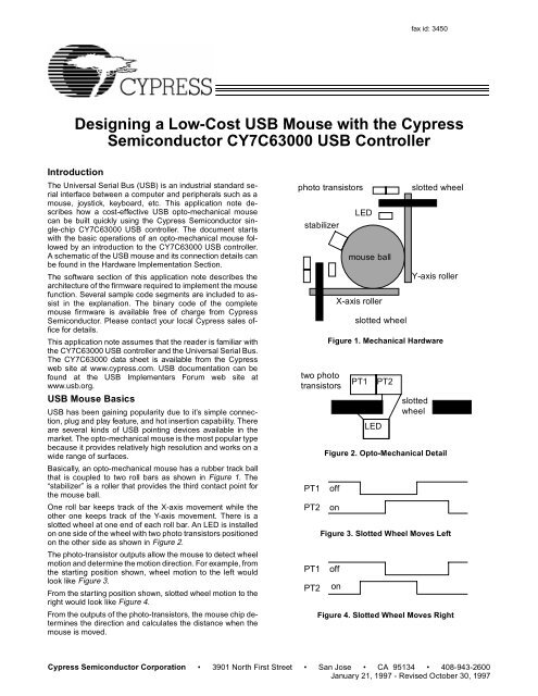
Basically, an opto-mechanical mouse has a rubber track ball<br />
that is coupled to two roll bars as shown in Figure 1. The<br />
“stabilizer” is a roller that provides <strong>the</strong> third contact point for<br />
<strong>the</strong> mouse ball.<br />
One roll bar keeps track of <strong>the</strong> X-axis movement while <strong>the</strong><br />
o<strong>the</strong>r one keeps track of <strong>the</strong> Y-axis movement. There is a<br />
slotted wheel at one end of each roll bar. An LED is installed<br />
on one side of <strong>the</strong> wheel <strong>with</strong> two photo transistors positioned<br />
on <strong>the</strong> o<strong>the</strong>r side as shown in Figure 2.<br />
The photo-transistor outputs allow <strong>the</strong> mouse to detect wheel<br />
motion and determine <strong>the</strong> motion direction. For example, from<br />
<strong>the</strong> starting position shown, wheel motion to <strong>the</strong> left would<br />
look like Figure 3.<br />
From <strong>the</strong> starting position shown, slotted wheel motion to <strong>the</strong><br />
right would look like Figure 4.<br />
From <strong>the</strong> outputs of <strong>the</strong> photo-transistors, <strong>the</strong> mouse chip determines<br />
<strong>the</strong> direction and calculates <strong>the</strong> distance when <strong>the</strong><br />
mouse is moved.<br />
photo transistors<br />
stabilizer<br />
two photo<br />
transistors<br />
PT1<br />
PT2<br />
PT1<br />
PT2<br />
LED<br />
mouse ball<br />
X-axis roller<br />
slotted wheel<br />
slotted wheel<br />
Y-axis roller<br />
Figure 1. Mechanical Hardware<br />
PT1<br />
LED<br />
PT2<br />
slotted<br />
wheel<br />
Figure 2. Opto-Mechanical Detail<br />
off<br />
on<br />
Figure 3. Slotted Wheel Moves Left<br />
off<br />
on<br />
Figure 4. Slotted Wheel Moves Right<br />
<strong>Cypress</strong> <strong>Semiconductor</strong> Corporation • 3901 North First Street • San Jose • CA 95134 • 408-943-2600<br />
January 21, 1997 - Revised October 30, 1997
<strong>Designing</strong> a <strong>Low</strong>-<strong>Cost</strong> <strong>USB</strong> <strong>Mouse</strong><br />
The resolution is <strong>the</strong> smallest motion <strong>the</strong> mouse can detect,<br />
measured in dots per inch (DPI). A typical opto-mechanical<br />
mouse has a resolution in <strong>the</strong> 200 to 400 DPI range. The<br />
mechanical dimensions of <strong>the</strong> mouse hardware limit <strong>the</strong> maximum<br />
achievable resolution.<br />
<strong>USB</strong> provides <strong>the</strong> plug-and-play feature that is not supported<br />
in RS-232 and PS/2 interfaces. The <strong>USB</strong> interface uses a<br />
four-pin connector <strong>with</strong> positive retention. A 28 AWG twisted<br />
pair is used for differential signaling and two 20 to 30 AWG<br />
wires are used to supply power and ground. No cable shielding<br />
is necessary for a mouse application.<br />
Introduction to CY7C63000<br />
The CY7C63000 is a high performance 8-bit RISC microcontroller<br />
<strong>with</strong> an integrated <strong>USB</strong> Serial Interface Engine (SIE).<br />
The architecture implements 34 commands that are optimized<br />
for <strong>USB</strong> applications. The CY7C63000 has built-in<br />
clock oscillator and timers as well as programmable current<br />
drivers, and pull-up resistors at each I/O line. High performance,<br />
low-cost human-interface type computer peripherals<br />
such as mouse, joystick, and gamepad can be implemented<br />
<strong>with</strong> minimum external components and firmware effort.<br />
Clock Circuit<br />
The CY7C63000 has a built-in clock oscillator and PLL-based<br />
frequency doubler. This circuit allows a cost effective 6 MHz<br />
ceramic resonator to be used externally while <strong>the</strong> on-chip<br />
RISC core runs at 12 MHz.<br />
<strong>USB</strong> Serial Interface Engine (SIE)<br />
The operation of <strong>the</strong> SIE is totally transparent to <strong>the</strong> user. In<br />
<strong>the</strong> receive mode, <strong>USB</strong> packet decode and data transfer to<br />
<strong>the</strong> endpoint FIFO are automatically done by <strong>the</strong> SIE. The SIE<br />
<strong>the</strong>n generates an interrupt request to invoke <strong>the</strong> service routine<br />
after a packet is unpacked.<br />
In <strong>the</strong> transmit mode, data transfer from <strong>the</strong> endpoint and <strong>the</strong><br />
assembly of <strong>the</strong> <strong>USB</strong> packet are handled automatically by <strong>the</strong><br />
SIE.<br />
General Purpose I/O<br />
The CY7C63000 has 12 general purpose I/O lines divided<br />
into 2 ports: Port 0 and Port 1. One such I/O circuit is shown<br />
in Figure 5. The output state can be programmed according<br />
to Table 1 below. Writing a “0” to <strong>the</strong> Data Register will drive<br />
<strong>the</strong> output <strong>Low</strong> and allow it to sink current.<br />
Table 1. Programmable Output State<br />
Port Data bit Port Pull-up bit Output State<br />
0 X sink current “0”<br />
1 0 pull-up resistor “1”<br />
1 1 High-Z<br />
Instead of supporting a fixed output drive, <strong>the</strong> CY7C63000<br />
allows <strong>the</strong> user to select an output current level for each I/O<br />
line. The sink current of each output is controlled by a dedicated<br />
8-bit Isink Register. The lower 4-bits of this register contains<br />
a code selecting one of sixteen sink current levels. The<br />
upper 4-bits are reserved and must be written as zeros. The<br />
output sink current levels of <strong>the</strong> two I/O ports are different. For<br />
Port 0 outputs, <strong>the</strong> lowest drive strength (0000) is about 0.2<br />
mA and <strong>the</strong> highest drive strength (1111) is about 1.0 mA.<br />
These levels are insufficient to drive <strong>the</strong> LEDs in a mouse.<br />
Port 1 outputs are specially designed to drive high-current<br />
applications such as LEDs. Each Port 1 output is much stronger<br />
than <strong>the</strong>ir Port 0 counterparts at <strong>the</strong> same drive level setting.<br />
In o<strong>the</strong>r words, <strong>the</strong> lowest and highest drive for Port 1<br />
lines are 3.2 mA and 16 mA respectively.<br />
Each General Purpose I/O (GPIO) is capable of generating<br />
an interrupt to <strong>the</strong> RISC core. Interrupt polarity is selectable<br />
on a per bit basis using <strong>the</strong> Port Pull-up register. Setting a Port<br />
Pull-up register bit to “1” will select a rising edge trigger for <strong>the</strong><br />
corresponding GPIO line. Conversely, setting a Port Pull-up<br />
Register bit to “0” will select a falling edge trigger. The interrupt<br />
triggered by a GPIO line is individually enabled by a dedicated<br />
bit in <strong>the</strong> Port Interrupt Enable Registers. All GPIO interrupts<br />
are fur<strong>the</strong>r masked by <strong>the</strong> Global GPIO Interrupt<br />
Enable Bit in <strong>the</strong> Global Interrupt Enable Register.<br />
V CC<br />
Port Pull-Up<br />
Register<br />
Port Data<br />
Register<br />
Schmitt<br />
Trigger<br />
16 KΩ<br />
GPIO<br />
Pin<br />
Data Bus<br />
Port Isink<br />
Register<br />
Isink<br />
DAC<br />
Figure 5. One General Purpose I/O Line<br />
2
<strong>Designing</strong> a <strong>Low</strong>-<strong>Cost</strong> <strong>USB</strong> <strong>Mouse</strong><br />
The Port Pull-up Registers are located at I/O address 0x08<br />
and 0x09 for Port 0 and Port 1 respectively. The Data Registers<br />
are located at I/O address 0x00 and 0x01 for Port 0 and<br />
Port 1 respectively. The Port 0 and Port 1 Interrupt Enable<br />
Registers are at addresses 0x04 and 0x05 respectively.<br />
Wake-Up Interrupt<br />
Power management is paramount in many <strong>USB</strong> applications.<br />
To conserve power, <strong>the</strong> CY7C63000 supports an externally<br />
programmable interrupt input to wake up <strong>the</strong> microcontroller<br />
from <strong>the</strong> suspend mode when <strong>the</strong> mouse is moved or when a<br />
button is pressed. The suspend mode causes <strong>the</strong> microcontroller<br />
to shut down most of its functions such as <strong>the</strong> clock<br />
circuit, <strong>the</strong> RISC core, <strong>the</strong> timer, and part of <strong>the</strong> SIE. In <strong>the</strong><br />
mouse application, a high percentage of <strong>the</strong> power is consumed<br />
by <strong>the</strong> LEDs. Therefore, <strong>the</strong> CY7C63000 should be<br />
programmed to turn off <strong>the</strong> LEDs before entering <strong>the</strong> suspend<br />
mode. With <strong>the</strong> LEDs off, <strong>the</strong> CY7C63000 can no longer detect<br />
any mouse movements although button closures are still<br />
recognized (because pressing a button causes an interrupt).<br />
This problem can be solved by using <strong>the</strong> wake-up interrupt<br />
that wakes up <strong>the</strong> microcontroller, checks for mouse movement,<br />
and <strong>the</strong>n goes back to suspend mode.<br />
The wake-up interrupt can be implemented by connecting <strong>the</strong><br />
CEXT pin to VCC <strong>with</strong> a resistor and to GND <strong>with</strong> a capacitor.<br />
Before <strong>the</strong> firmware puts <strong>the</strong> microcontroller into <strong>the</strong> suspend<br />
mode, it writes a zero to <strong>the</strong> Cext register at address 0x22 to<br />
discharge <strong>the</strong> external capacitor. Then, to start timing a one<br />
is written to <strong>the</strong> Cext register to allow <strong>the</strong> RC circuit to begin<br />
charging. A wake-up interrupt is generated to <strong>the</strong> RISC core<br />
when <strong>the</strong> external capacitor is charged up to nominal 2.75V<br />
(45% to 65% of Vcc) by <strong>the</strong> external resistor. The duration<br />
between successive wake-ups is controlled by <strong>the</strong> RC constant<br />
of <strong>the</strong> external resistor and capacitor.<br />
Hardware Implementation<br />
Figure 6 is <strong>the</strong> schematic for a mouse application.<br />
Photo transistor pins of Port 0 are programmed by writing a<br />
zero to <strong>the</strong> Data Registers which drives <strong>the</strong> output low. Then<br />
set <strong>the</strong> value of <strong>the</strong> Port Isink Register to <strong>the</strong> sink current<br />
value. One of sixteen sink current values could be selected.<br />
This is done to bias <strong>the</strong> photo transistors for correct operation.<br />
Button pins of Port 0 are programmed to accept active-low<br />
inputs <strong>with</strong> internal pull-up resistors enabled. This is accomplished<br />
by setting all bits in <strong>the</strong> Port 0 Data Register to “1” and<br />
setting <strong>the</strong> contents of <strong>the</strong> Port 0 Pull-up Register to all “0”s.<br />
Bits 4 to 6 of Port 0 are connected to <strong>the</strong> left, right, and middle<br />
buttons respectively. Bits 0 and 1 are connected to <strong>the</strong> left and<br />
right photo transistors of <strong>the</strong> horizontal axis respectively. Bits<br />
2 and 3 are connected to left and right photo transistors of <strong>the</strong><br />
vertical axis respectively.<br />
The two LEDs are connected in series to bit 0 of Port 1. The<br />
LEDs are turned off in <strong>the</strong> suspend mode to conserve power.<br />
The LEDs are switched on only when <strong>the</strong> mouse wakes up.<br />
Because <strong>the</strong> sink current of each GPIO line can be set to one<br />
of sixteen levels, <strong>the</strong> user can adjust <strong>the</strong> light output of <strong>the</strong><br />
LEDs to match <strong>the</strong> sensitivity of a wide range of photo transistors.<br />
The CEXT pin of <strong>the</strong> CY7C63000 is connected to an external<br />
RC timing circuit formed by R2 and C1. The wake-up time is<br />
set to about 20 msec to achieve a good balance between<br />
wake-up response time and power savings.<br />
A 6 MHz ceramic resonator is connected to <strong>the</strong> clock inputs<br />
of <strong>the</strong> microcontroller. This component should be placed as<br />
close to <strong>the</strong> microcontroller as possible.<br />
According to <strong>the</strong> <strong>USB</strong> specification, <strong>the</strong> <strong>USB</strong> D– line of a<br />
low-speed device (1.5 Mbps) should be tied to a voltage<br />
source between 3.0V and 3.6V <strong>with</strong> a 1.5K ohms pull-up terminator.<br />
The CY7C63000 eliminates <strong>the</strong> need for a 3.3V regulator<br />
by specifying a 7.5 Kohm resistor connected between<br />
<strong>the</strong> <strong>USB</strong> D– line and <strong>the</strong> nominal 5V Vcc.<br />
3
<strong>Designing</strong> a <strong>Low</strong>-<strong>Cost</strong> <strong>USB</strong> <strong>Mouse</strong><br />
Figure 6. Hardware Implementation<br />
4
<strong>Designing</strong> a <strong>Low</strong>-<strong>Cost</strong> <strong>USB</strong> <strong>Mouse</strong><br />
Firmware Implementation<br />
<strong>USB</strong> Interface<br />
All <strong>USB</strong> Human Interface Device (HID) class applications<br />
such as a mouse, follow <strong>the</strong> same <strong>USB</strong> start-up procedure.<br />
The procedure is as follows (see Figure 7):<br />
Device Plug-in<br />
Start<br />
• Set up stack pointer<br />
• Enable all interrupts being used<br />
Bus Reset<br />
Main Loop<br />
Enumeration<br />
Figure 8. Reset Interrupt Service Routine<br />
Data Acquisition/<br />
Transfer<br />
Figure 7. <strong>USB</strong> Start-Up Procedure<br />
End Point 0<br />
Device Plug-in<br />
When a <strong>USB</strong> device is first connected to <strong>the</strong> bus, it is powered<br />
but remains non-functional waiting for a bus reset. The pull-up<br />
resistor on D– notifies <strong>the</strong> hub that a low-speed (1.5 Mbps)<br />
device has just been connected.<br />
Bus Reset<br />
The host recognizes <strong>the</strong> presence of a new <strong>USB</strong> device and<br />
resets it (see Figure 8).<br />
Enumeration<br />
The host sends a SETUP packet followed by IN packets to<br />
read <strong>the</strong> device description from default address 0. When <strong>the</strong><br />
description is received, <strong>the</strong> host assigns a new <strong>USB</strong> address<br />
to <strong>the</strong> device. The device begins responding to communication<br />
<strong>with</strong> <strong>the</strong> newly assigned address, while <strong>the</strong> host continues<br />
to ask for information about <strong>the</strong> device description, configuration<br />
description and HID report description. Using <strong>the</strong><br />
information returned from <strong>the</strong> device, <strong>the</strong> host now knows <strong>the</strong><br />
number of data endpoints supported by <strong>the</strong> device (in a <strong>USB</strong><br />
mouse, <strong>the</strong>re is only one data endpoint). At this point, <strong>the</strong><br />
process of enumeration is completed. See Figures 9, 10 and<br />
11.<br />
received a<br />
SETUP packet<br />
• Responds to<br />
SETUP packet<br />
according to <strong>the</strong><br />
parsing structure<br />
return<br />
Y<br />
N<br />
Figure 9. Endpoint 0 ISR<br />
5
<strong>Designing</strong> a <strong>Low</strong>-<strong>Cost</strong> <strong>USB</strong> <strong>Mouse</strong><br />
bmrequest type<br />
host to dev<br />
dev recip<br />
0x00<br />
host to dev<br />
inter recip<br />
0x01<br />
host to dev<br />
endp recip<br />
0x02<br />
dev to host<br />
dev recip<br />
0x80<br />
dev to host<br />
inter recip<br />
0x81<br />
dev to host<br />
endp recip<br />
0x82<br />
get status<br />
0x00<br />
clr feature<br />
0x01<br />
set feature<br />
0x3<br />
set addr<br />
0x05<br />
get desc<br />
0x06<br />
set desc<br />
0x07<br />
get config<br />
0x08<br />
set config<br />
0x09<br />
get inter<br />
0x0A<br />
set inter<br />
0x0B<br />
synch<br />
0x0C<br />
brequest<br />
Figure 10. <strong>USB</strong> Standard Request Parsing Structure<br />
bmrequest type<br />
host to dev<br />
inter recip<br />
0x21<br />
dev to host<br />
inter recip<br />
0xA1<br />
get_reportl<br />
0x01<br />
get_idle<br />
0x02<br />
get_protocol<br />
0x03<br />
set_reportl<br />
0x09<br />
set_idle<br />
0x0A<br />
set_protocol<br />
0x0B<br />
brequest<br />
Figure 11. <strong>USB</strong> HID Class Request Parsing Structure<br />
Data Acquisition/Transfer<br />
The firmware polls <strong>the</strong> mouse buttons and <strong>the</strong> photo transistors.<br />
The status of <strong>the</strong> buttons as well as <strong>the</strong> horizontal and<br />
vertical displacements are sent to <strong>the</strong> host using endpoint 1.<br />
When <strong>the</strong> host issues IN packets to retrieve data from <strong>the</strong><br />
device, <strong>the</strong> device returns three bytes of data as shown in<br />
Figure 12. Figure 13 illustrates response to an e14, and 15.)<br />
Bit 7 Bit 0<br />
N/A N/A N/A N/A N/A Mid Right Left Byte 0 - buttons<br />
Bit 7 Bit 0<br />
HD7 HD6 HD5 HD4 HD3 HD2 HD1 HD0 Byte 1 - Horizontal<br />
displacement<br />
Bit 7 Bit 0<br />
VD7 VD6 VD5 VD4 VD3 VD2 VD1 VD0 Byte 2 - Vertical<br />
displacement<br />
Figure 12. Data Organization for <strong>USB</strong> <strong>Mouse</strong><br />
6
<strong>Designing</strong> a <strong>Low</strong>-<strong>Cost</strong> <strong>USB</strong> <strong>Mouse</strong><br />
Endpoint_1<br />
• Prepare data in Endpoint_1 DMA<br />
buffer<br />
• Re-enable interrupts<br />
Return<br />
Figure 13. Endpoint 1 Interrupt Service Routine<br />
lh = left horizontal photo transistor<br />
rh = right horizontal photo transistor<br />
r/l = right / left bit state<br />
r/l=0 0<br />
lh=0<br />
STATE 0<br />
rh=0<br />
r/l=01<br />
STATE 1<br />
rh=01<br />
lh=1 rh=1<br />
rh=10 lh=10<br />
STATE 3<br />
lh=01<br />
STATE 2<br />
r/l=10<br />
r/l=11<br />
Figure 14. <strong>Mouse</strong> State Diagram<br />
State 3 State 2 State 0 State 1 State 3<br />
Left horizontal<br />
photo transistor output<br />
Right horizontal<br />
photo transistor output<br />
Left movement Right movement<br />
Figure 15. State Definitions<br />
7
<strong>Designing</strong> a <strong>Low</strong>-<strong>Cost</strong> <strong>USB</strong> <strong>Mouse</strong><br />
The byte order and bit field positions are defined by <strong>the</strong> <strong>USB</strong><br />
HID specification.<br />
<strong>USB</strong> Descriptors<br />
As stated earlier, <strong>the</strong> <strong>USB</strong> descriptors hold information about<br />
<strong>the</strong> device. There are several types of descriptors, which will<br />
be discussed in detail below. All descriptors have certain<br />
characteristics in common. Byte 0 is always <strong>the</strong> descriptor<br />
length in bytes and Byte 1 is always <strong>the</strong> descriptor type. Discussion<br />
of <strong>the</strong>se two bytes will be omitted from <strong>the</strong> following<br />
descriptions. The rest of <strong>the</strong> descriptor structure is dependent<br />
on <strong>the</strong> descriptor type. An example of each descriptor will be<br />
given. Descriptor types are device, configuration, interface,<br />
endpoint, string, report, and several different class descriptors.<br />
Device Descriptor<br />
This is <strong>the</strong> first descriptor <strong>the</strong> host requests from <strong>the</strong> device.<br />
It contains important information about <strong>the</strong> device. The size<br />
of this descriptor is 18 bytes. A list follows:<br />
• <strong>USB</strong> Specification release number in binary-coded decimal<br />
(BCD) (2 bytes)<br />
• Device class (1 byte)<br />
• Device subclass (1 byte)<br />
• Device protocol (1 byte)<br />
• Max packet size for Endpoint 0 (1 byte)<br />
• Vendor ID (2 bytes)<br />
• Product ID (2 bytes)<br />
• Device release number in BCD (2 bytes)<br />
• Index of string describing Manufacturer (Optional) (1 byte)<br />
• Index of string describing Product (Optional) (1 byte)<br />
• Index of string containing serial number (Optional) (1 byte)<br />
• Number of configurations for <strong>the</strong> device (1 byte)<br />
Example of a device descriptor<br />
Descriptor Length (18 bytes)<br />
Descriptor Type (Device)<br />
Complies to <strong>USB</strong> Spec Release (1.00)<br />
Class Code (insert code)<br />
Subclass Code (0)<br />
Protocol (No specific protocol)<br />
Max Packet Size for endpt 0 (8 bytes)<br />
Vendor ID (<strong>Cypress</strong>)<br />
Product ID (<strong>USB</strong> Joystick)<br />
Device Release Number (1.03)<br />
String Describing Vendor (None)<br />
String Describing Product (None)<br />
String for Serial Number (None)<br />
Possible Configurations (1)<br />
Configuration Descriptor<br />
The configuration descriptor is 9 bytes in length and gives <strong>the</strong><br />
configuration information for <strong>the</strong> device. It is possible to have<br />
more than one configuration for each device. When <strong>the</strong> host<br />
requests a configuration descriptor, it will continue to read<br />
<strong>the</strong>se descriptors until all configurations have been received.<br />
A list of <strong>the</strong> structure follows:<br />
• Total length of <strong>the</strong> data returned for this configuration (2<br />
bytes)<br />
• Number of interfaces for this configuration (1 byte)<br />
• Value used to address this configuration (1 byte)<br />
• Index of string describing this configuration (Optional) (1<br />
byte)<br />
• Attributes bitmap describing configuration characteristics<br />
(1 byte)<br />
• Maximum power <strong>the</strong> device will consume from <strong>the</strong> bus (1<br />
byte)<br />
Example of configuration descriptor<br />
Descriptor Length (9 bytes)<br />
Descriptor Type (Configuration)<br />
Total Data Length (34 bytes)<br />
Interfaces Supported (1)<br />
Configuration Value (1)<br />
String Describing this Config (None)<br />
Config Attributes (Bus powered)<br />
Max Bus Power Consumption (100mA)<br />
Interface Descriptor<br />
The interface descriptor is 9 bytes long and describes <strong>the</strong><br />
interface of each device. It is possible to have more than one<br />
interface for each device. This descriptor is set up as follows:<br />
• Number of this interface (1 byte)<br />
• Value used to select alternate setting for this interface (1<br />
byte)<br />
• Number of endpoints used by this interface. If this number<br />
is zero, only endpoint 0 is used by this interface (1 byte)<br />
• Class code (1 byte)<br />
• Subclass code (1 byte)<br />
• Protocol code (1 byte)<br />
• Index of string describing this interface (1 byte)<br />
Example of interface descriptor<br />
Descriptor Length (9 bytes)<br />
Descriptor Type (Interface)<br />
Interface Number (0)<br />
Alternate Setting (0)<br />
Number of Endpoints (1)<br />
Class Code (insert code)<br />
Subclass Code (0)<br />
Protocol (No specific protocol)<br />
String Describing Interface (None)<br />
Endpoint Descriptor<br />
The endpoint descriptor describes each endpoint, including<br />
<strong>the</strong> attributes and <strong>the</strong> address of each endpoint. It is possible<br />
to have more than one endpoint for each interface. This descriptor<br />
is 7 bytes long and is set up as follows:<br />
• Endpoint address (1 byte)<br />
• Endpoint attributes. Describes transfer type (1 byte)<br />
• Maximum packet size this endpoint is capable of transferring<br />
(2 bytes)<br />
• Time interval at which this endpoint will be polled for data<br />
(1 byte)<br />
Example of endpoint descriptor<br />
Descriptor Length (7 bytes)<br />
Descriptor Type (Endpoint)<br />
8
<strong>Designing</strong> a <strong>Low</strong>-<strong>Cost</strong> <strong>USB</strong> <strong>Mouse</strong><br />
Endpoint Address (IN, Endpoint 1)<br />
Attributes (Interrupt)<br />
Maximum Packet Size (6 bytes)<br />
Polling Interval (10 ms)<br />
HID (Class) Descriptor<br />
The class descriptor tells <strong>the</strong> host about <strong>the</strong> class of <strong>the</strong> device.<br />
In this case, <strong>the</strong> device falls in <strong>the</strong> human interface device<br />
(HID) class. This descriptor is 9 bytes in length and is set<br />
up as follows:<br />
• Class release number in BCD (2 bytes)<br />
• Localized country code (1 byte)<br />
• Number of HID class descriptor to follow (1 byte)<br />
• Report descriptor type (1 byte)<br />
• Total length of report descriptor in bytes (2 bytes)<br />
Example of HID class descriptor<br />
Descriptor Length (9 bytes)<br />
Descriptor Type (HID Class)<br />
HID Class Release Number (1.00)<br />
Localized Country Code (USA)<br />
Number of Descriptors (1)<br />
Report Descriptor Type (HID)<br />
Report Descriptor Length (63 bytes)<br />
Report Descriptor<br />
This is <strong>the</strong> most complicated descriptor in <strong>USB</strong>. There is no<br />
set structure. It is more like a computer language that describes<br />
<strong>the</strong> format of <strong>the</strong> device’s data in detail. This descriptor<br />
is used to define <strong>the</strong> structure of <strong>the</strong> data returned to <strong>the</strong><br />
host as well as to tell <strong>the</strong> host what to do <strong>with</strong> that data. An<br />
example of a report descriptor can be found below.<br />
A report descriptor must contain <strong>the</strong> following items: Input (or<br />
Output or Feature), Usage, Usage Page, Logical Minimum,<br />
Logical Maximum, Report size, and Report Count. These are<br />
all necessary to describe <strong>the</strong> device’s data.<br />
Example of report descriptor<br />
Usage Page (Generic Desktop)<br />
Usage (<strong>Mouse</strong>)<br />
Collection (Application)<br />
Usage (Pointer)<br />
Collection (Physical)<br />
Usage Page (Buttons)<br />
Usage Minimum (01)<br />
Usage Maximum (03)<br />
Logical Minimum (0)<br />
Logical Maximum (1)<br />
Report Count (3)<br />
Report Size (1)<br />
Input (Data, Variable,<br />
Absolute)<br />
Report Count (1)<br />
Report Size (5)<br />
Input (Constant)<br />
Usage Page (Generic Desktop)<br />
Usage (X)<br />
Usage (Y)<br />
Logical Minimum (-127)<br />
Logical Maximum (127)<br />
Report Size (8)<br />
Report Count (2)<br />
Input (Data, Variable,<br />
Variable)<br />
End Collection<br />
End Collection<br />
Input items are used to tell <strong>the</strong> host what type of data will be<br />
returned as input to <strong>the</strong> host for interpretation. These items<br />
describe attributes such as data vs. constant, variable vs. array,<br />
absolute vs. relative, etc.<br />
Usages are <strong>the</strong> part of <strong>the</strong> descriptor that defines what should<br />
be done <strong>with</strong> <strong>the</strong> data that is returned to <strong>the</strong> host. From <strong>the</strong><br />
example descriptor, Usage (X) tells <strong>the</strong> host that <strong>the</strong> data is<br />
to be used as an X axis input. There is also ano<strong>the</strong>r kind of<br />
Usage tag found in <strong>the</strong> example called a Usage Page. The<br />
reason for <strong>the</strong> Usage Page is that it is necessary to allow for<br />
more than 256 possible Usage tags. Usage Page tags are<br />
used as a second byte which allows for up to 65536 Usages.<br />
Logical Minimum and Logical Maximum are used to bound<br />
<strong>the</strong> values that a device will return.<br />
Report Size and Report Count define <strong>the</strong> structures that <strong>the</strong><br />
data will be transferred in. Report Size gives <strong>the</strong> size of <strong>the</strong><br />
structure in bits. Report Count defines how many structures<br />
will be used. In <strong>the</strong> example descriptor above, <strong>the</strong> lines Report<br />
Size (8) and Report Count (2) define <strong>the</strong> axes of <strong>the</strong><br />
mouse. There are now two eight-bit fields defined, one for <strong>the</strong><br />
X axis and one for <strong>the</strong> Y axis.<br />
Collection items are used to show a relationship between two<br />
or more sets of data. End Collection items simply close <strong>the</strong><br />
collection.<br />
It is important to note that all examples given here are merely<br />
for clarification. They are not necessarily definitive solutions.<br />
A more detailed description of all items discussed here as<br />
well as o<strong>the</strong>r descriptor issues can be found in <strong>the</strong> “Device<br />
Class Definition for Human Interface Devices (HID)” revision<br />
1.0d and in <strong>the</strong> “Universal Serial Bus Specification” revision<br />
1.0, chapter 9. Both of <strong>the</strong>se documents can be found on <strong>the</strong><br />
<strong>USB</strong> world wide web site at http://www.usb.org/.<br />
Power Management<br />
Power management on <strong>USB</strong> devices involves <strong>the</strong> issues described<br />
in Figures 16 and 17. The LEDs are turned off before<br />
<strong>the</strong> device goes into suspend and are turned on right after <strong>the</strong><br />
device gets out of suspend.<br />
Displacement Calculation<br />
The outputs of <strong>the</strong> photo transistors for one axis transition<br />
through <strong>the</strong> states shown in Figure 14. A transition from one<br />
state to <strong>the</strong> next indicates mouse movement in that direction.<br />
Based on <strong>the</strong> position of <strong>the</strong> photo transistors, a<br />
counter-clockwise state change increments <strong>the</strong> mouse position<br />
counter and a clockwise state change decrements <strong>the</strong><br />
position counter. The displacements are calculated based on<br />
<strong>the</strong> previous location of <strong>the</strong> mouse.<br />
Conclusion<br />
The two main enabling factors of <strong>the</strong> proliferation of <strong>the</strong> <strong>USB</strong><br />
devices are cost and functionality. The CY7C63000 meets<br />
both requirements by integrating <strong>the</strong> <strong>USB</strong> SIE and multi-function<br />
I/Os <strong>with</strong> a <strong>USB</strong> optimized RISC core.<br />
9
<strong>Designing</strong> a <strong>Low</strong>-<strong>Cost</strong> <strong>USB</strong> <strong>Mouse</strong><br />
1 ms<br />
• Clear watchdog<br />
timer<br />
Y<br />
Remote<br />
Wakeup<br />
process?<br />
• Increment 10 msec wakeup<br />
counter<br />
N<br />
<strong>USB</strong> bus<br />
activity<br />
N<br />
Y<br />
• Load software counter<br />
• Clear bus activity bit<br />
• Decrement software<br />
counter<br />
N<br />
software<br />
counter = 0<br />
Y<br />
• Enable global interrupts except Cext<br />
and 128 µs<br />
Remote<br />
Wakeup<br />
Enabled?<br />
N<br />
Y<br />
return<br />
•Clear Cext<br />
• Set Cext to High-Z<br />
• Enable Cext interrupts<br />
• Load software counter<br />
• Suspend µC and wait for interrupts<br />
Figure 16. One msec Interrupt Service Routine<br />
10
<strong>Designing</strong> a <strong>Low</strong>-<strong>Cost</strong> <strong>USB</strong> <strong>Mouse</strong><br />
Remote Wake-Up<br />
Clear Cext<br />
Compare Port 0 value<br />
to stored Port 0 value<br />
Check for mouse or a button press<br />
Same<br />
Y<br />
If same, no mouse movement<br />
N<br />
Write RESUME bit<br />
03h to <strong>USB</strong> Status and<br />
Control reg.<br />
If different, wake-up host<br />
Loop for 10 ms<br />
(remember to reset<br />
WD timer)<br />
Send resume signal for 10 ms<br />
Clear RESUME bit<br />
write 00h to <strong>USB</strong> Status<br />
and Control reg<br />
Set Cext to High Z<br />
Return<br />
Figure 17. Remote Wake-Up Interrupt<br />
© <strong>Cypress</strong> <strong>Semiconductor</strong> Corporation, 1997. The information contained herein is subject to change <strong>with</strong>out notice. <strong>Cypress</strong> <strong>Semiconductor</strong> Corporation assumes no responsibility for <strong>the</strong> use<br />
of any circuitry o<strong>the</strong>r than circuitry embodied in a <strong>Cypress</strong> <strong>Semiconductor</strong> product. Nor does it convey or imply any license under patent or o<strong>the</strong>r rights. <strong>Cypress</strong> <strong>Semiconductor</strong> does not authorize<br />
its products for use as critical components in life-support systems where a malfunction or failure may reasonably be expected to result in significant injury to <strong>the</strong> user. The inclusion of <strong>Cypress</strong><br />
<strong>Semiconductor</strong> products in life-support systems application implies that <strong>the</strong> manufacturer assumes all risk of such use and in doing so indemnifies <strong>Cypress</strong> <strong>Semiconductor</strong> against all charges.