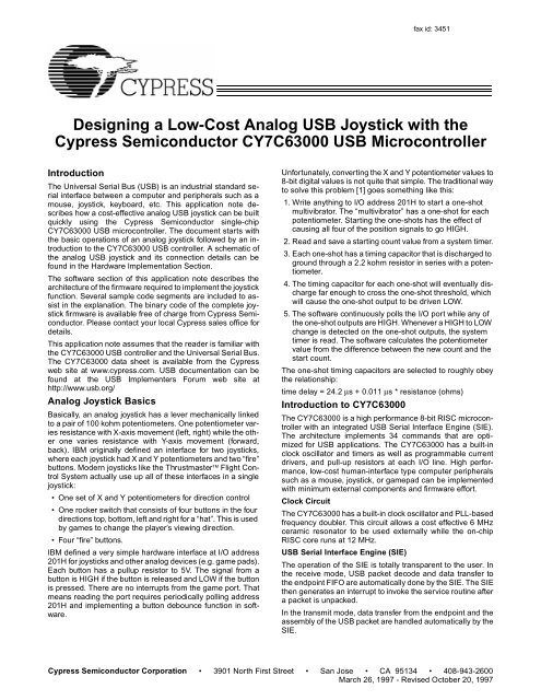
Designing a Low-Cost Analog USB Joystick with the Cypress ...
Designing a Low-Cost Analog USB Joystick with the Cypress ...
Designing a Low-Cost Analog USB Joystick with the Cypress ...

You also want an ePaper? Increase the reach of your titles
YUMPU automatically turns print PDFs into web optimized ePapers that Google loves.
fax id: 3451<br />
<strong>Designing</strong> a <strong>Low</strong>-<strong>Cost</strong> <strong>Analog</strong> <strong>USB</strong> <strong>Joystick</strong> <strong>with</strong> <strong>the</strong><br />
<strong>Cypress</strong> Semiconductor CY7C63000 <strong>USB</strong> Microcontroller<br />
Introduction<br />
The Universal Serial Bus (<strong>USB</strong>) is an industrial standard serial<br />
interface between a computer and peripherals such as a<br />
mouse, joystick, keyboard, etc. This application note describes<br />
how a cost-effective analog <strong>USB</strong> joystick can be built<br />
quickly using <strong>the</strong> <strong>Cypress</strong> Semiconductor single-chip<br />
CY7C63000 <strong>USB</strong> microcontroller. The document starts <strong>with</strong><br />
<strong>the</strong> basic operations of an analog joystick followed by an introduction<br />
to <strong>the</strong> CY7C63000 <strong>USB</strong> controller. A schematic of<br />
<strong>the</strong> analog <strong>USB</strong> joystick and its connection details can be<br />
found in <strong>the</strong> Hardware Implementation Section.<br />
The software section of this application note describes <strong>the</strong><br />
architecture of <strong>the</strong> firmware required to implement <strong>the</strong> joystick<br />
function. Several sample code segments are included to assist<br />
in <strong>the</strong> explanation. The binary code of <strong>the</strong> complete joystick<br />
firmware is available free of charge from <strong>Cypress</strong> Semiconductor.<br />
Please contact your local <strong>Cypress</strong> sales office for<br />
details.<br />
This application note assumes that <strong>the</strong> reader is familiar <strong>with</strong><br />
<strong>the</strong> CY7C63000 <strong>USB</strong> controller and <strong>the</strong> Universal Serial Bus.<br />
The CY7C63000 data sheet is available from <strong>the</strong> <strong>Cypress</strong><br />
web site at www.cypress.com. <strong>USB</strong> documentation can be<br />
found at <strong>the</strong> <strong>USB</strong> Implementers Forum web site at<br />
http://www.usb.org/<br />
<strong>Analog</strong> <strong>Joystick</strong> Basics<br />
Basically, an analog joystick has a lever mechanically linked<br />
to a pair of 100 kohm potentiometers. One potentiometer varies<br />
resistance <strong>with</strong> X-axis movement (left, right) while <strong>the</strong> o<strong>the</strong>r<br />
one varies resistance <strong>with</strong> Y-axis movement (forward,<br />
back). IBM originally defined an interface for two joysticks,<br />
where each joystick had X and Y potentiometers and two “fire”<br />
buttons. Modern joysticks like <strong>the</strong> Thrustmaster Flight Control<br />
System actually use up all of <strong>the</strong>se interfaces in a single<br />
joystick:<br />
• One set of X and Y potentiometers for direction control<br />
• One rocker switch that consists of four buttons in <strong>the</strong> four<br />
directions top, bottom, left and right for a “hat”. This is used<br />
by games to change <strong>the</strong> player’s viewing direction.<br />
• Four “fire” buttons.<br />
IBM defined a very simple hardware interface at I/O address<br />
201H for joysticks and o<strong>the</strong>r analog devices (e.g. game pads).<br />
Each button has a pullup resistor to 5V. The signal from a<br />
button is HIGH if <strong>the</strong> button is released and LOW if <strong>the</strong> button<br />
is pressed. There are no interrupts from <strong>the</strong> game port. That<br />
means reading <strong>the</strong> port requires periodically polling address<br />
201H and implementing a button debounce function in software.<br />
Unfortunately, converting <strong>the</strong> X and Y potentiometer values to<br />
8-bit digital values is not quite that simple. The traditional way<br />
to solve this problem [1] goes something like this:<br />
1. Write anything to I/O address 201H to start a one-shot<br />
multivibrator. The “multivibrator” has a one-shot for each<br />
potentiometer. Starting <strong>the</strong> one-shots has <strong>the</strong> effect of<br />
causing all four of <strong>the</strong> position signals to go HIGH.<br />
2. Read and save a starting count value from a system timer.<br />
3. Each one-shot has a timing capacitor that is discharged to<br />
ground through a 2.2 kohm resistor in series <strong>with</strong> a potentiometer.<br />
4. The timing capacitor for each one-shot will eventually discharge<br />
far enough to cross <strong>the</strong> one-shot threshold, which<br />
will cause <strong>the</strong> one-shot output to be driven LOW.<br />
5. The software continuously polls <strong>the</strong> I/O port while any of<br />
<strong>the</strong> one-shot outputs are HIGH. Whenever a HIGH to LOW<br />
change is detected on <strong>the</strong> one-shot outputs, <strong>the</strong> system<br />
timer is read. The software calculates <strong>the</strong> potentiometer<br />
value from <strong>the</strong> difference between <strong>the</strong> new count and <strong>the</strong><br />
start count.<br />
The one-shot timing capacitors are selected to roughly obey<br />
<strong>the</strong> relationship:<br />
time delay = 24.2 µs + 0.011 µs * resistance (ohms)<br />
Introduction to CY7C63000<br />
The CY7C63000 is a high performance 8-bit RISC microcontroller<br />
<strong>with</strong> an integrated <strong>USB</strong> Serial Interface Engine (SIE).<br />
The architecture implements 34 commands that are optimized<br />
for <strong>USB</strong> applications. The CY7C63000 has a built-in<br />
clock oscillator and timers as well as programmable current<br />
drivers, and pull-up resistors at each I/O line. High performance,<br />
low-cost human-interface type computer peripherals<br />
such as a mouse, joystick, or gamepad can be implemented<br />
<strong>with</strong> minimum external components and firmware effort.<br />
Clock Circuit<br />
The CY7C63000 has a built-in clock oscillator and PLL-based<br />
frequency doubler. This circuit allows a cost effective 6 MHz<br />
ceramic resonator to be used externally while <strong>the</strong> on-chip<br />
RISC core runs at 12 MHz.<br />
<strong>USB</strong> Serial Interface Engine (SIE)<br />
The operation of <strong>the</strong> SIE is totally transparent to <strong>the</strong> user. In<br />
<strong>the</strong> receive mode, <strong>USB</strong> packet decode and data transfer to<br />
<strong>the</strong> endpoint FIFO are automatically done by <strong>the</strong> SIE. The SIE<br />
<strong>the</strong>n generates an interrupt to invoke <strong>the</strong> service routine after<br />
a packet is unpacked.<br />
In <strong>the</strong> transmit mode, data transfer from <strong>the</strong> endpoint and <strong>the</strong><br />
assembly of <strong>the</strong> <strong>USB</strong> packet are handled automatically by <strong>the</strong><br />
SIE.<br />
<strong>Cypress</strong> Semiconductor Corporation • 3901 North First Street • San Jose • CA 95134 • 408-943-2600<br />
March 26, 1997 - Revised October 20, 1997
<strong>Designing</strong> a <strong>Low</strong>-<strong>Cost</strong> <strong>USB</strong> <strong>Joystick</strong><br />
V CC<br />
Port Pull-Up<br />
Register<br />
Port Data<br />
Register<br />
Schmitt<br />
Trigger<br />
16 KΩ<br />
GPIO<br />
Pin<br />
Data Bus<br />
Port Isink<br />
Register<br />
Isink<br />
DAC<br />
Figure 1. One General Purpose I/O Line<br />
General Purpose I/O<br />
The CY7C63000 has 12 general purpose I/O lines divided<br />
into 2 ports: Port 0 and Port 1. One such I/O circuit is shown<br />
in Figure 1. The output state can be programmed according<br />
to Table 1 below. Writing a “0” to <strong>the</strong> Data Register will drive<br />
<strong>the</strong> output <strong>Low</strong> and allow it to sink current.<br />
Table 1. Programmable Output State<br />
Port Data bit Port Pull-up bit Output State<br />
0 X sink current “0”<br />
1 0 pull-up resistor “1”<br />
1 1 High-Z<br />
Instead of supporting a fixed output drive, <strong>the</strong> CY7C63000<br />
allows <strong>the</strong> user to select an output current level for each I/O<br />
line. The sink current of each output is controlled by a dedicated<br />
8-bit Isink Register. The lower 4-bits of this register contains<br />
a code selecting one of sixteen sink current levels. The<br />
upper 4-bits are reserved and must be written as zeros. The<br />
output sink current levels of <strong>the</strong> two I/O ports are different. For<br />
Port 0 outputs, <strong>the</strong> lowest drive strength (0000) is about 0.2<br />
mA and <strong>the</strong> highest drive strength (1111) is about 1.0 mA.<br />
These levels are insufficient to drive LEDs.<br />
Port 1 outputs are specially designed to drive high-current<br />
applications such as LEDs. Each Port 1 output is much stronger<br />
than its Port 0 counterparts at <strong>the</strong> same drive level setting.<br />
In o<strong>the</strong>r words, <strong>the</strong> lowest and highest drive for Port 1 lines<br />
are about 3.2 mA and 16 mA respectively.<br />
Each General Purpose I/O (GPIO) is capable of generating<br />
an interrupt to <strong>the</strong> RISC core. Interrupt polarity is selectable<br />
on a per bit basis using <strong>the</strong> Port Pull-up register. Setting a Port<br />
Pull-up register bit to “1” will select a rising edge trigger for <strong>the</strong><br />
corresponding GPIO line. Conversely, setting a Port Pull-up<br />
Register bit to “0” will select a falling edge trigger. The interrupt<br />
triggered by a GPIO line is individually enabled by a dedicated<br />
bit in <strong>the</strong> Interrupt Enable Register. All GPIO interrupts<br />
are fur<strong>the</strong>r masked by <strong>the</strong> Global GPIO Interrupt Enable Bit<br />
in <strong>the</strong> Global Interrupt Enable Register<br />
The Port Pull-up Registers are located at I/O address 0x08<br />
and 0x09 for Port 0 and Port 1 respectively. The Data Registers<br />
are located at I/O address 0x00 and 0x01 for Port 0 and<br />
Port 1 respectively.<br />
Hardware Implementation<br />
Figure 2 is <strong>the</strong> schematic for a joystick application.<br />
All I/O pins of Port 0 are programmed to accept active-low<br />
inputs <strong>with</strong> internal pull-up resistors enabled. This is accomplished<br />
by setting all bits in <strong>the</strong> Port 0 Data Register to “1” and<br />
setting <strong>the</strong> contents of <strong>the</strong> Port 0 Pull-up Register to all “0”s.<br />
Bits 0 to 3 of Port 0 are used to support up to four “fire” buttons.<br />
The only external components are <strong>the</strong> four buttons.<br />
Bits 4 to 7 of Port 0 are used to support a “hat” function. The<br />
hat is limited to nine possible positions. In <strong>the</strong> left to right<br />
direction, <strong>the</strong> X value can be maximum left, centered, or maximum<br />
right. In <strong>the</strong> forward and back direction, <strong>the</strong> Y value can<br />
be maximum forward, centered, or maximum back. Again,<br />
<strong>the</strong>re are no external components except <strong>the</strong> buttons.<br />
Bits 0, 1, and 2 of Port 1 are used to read <strong>the</strong> X, Y, and<br />
THROTTLE potentiometers respectively. The only external<br />
components needed are a 1800 pF capacitor and a 2Kohm<br />
resistor for each axis.<br />
A 6 MHz ceramic resonator is connected to <strong>the</strong> clock inputs<br />
of <strong>the</strong> microcontroller. This component should be placed as<br />
close to <strong>the</strong> microcontroller as possible.<br />
According to <strong>the</strong> <strong>USB</strong> specification, <strong>the</strong> <strong>USB</strong> D– line of a<br />
low-speed device (1.5 Mbps) should be tied to a voltage<br />
source between 3.0V and 3.6V <strong>with</strong> a 1.5K ohms pull-up terminator.<br />
The CY7C63000 eliminates <strong>the</strong> need for a 3.3V regulator<br />
by specifying a 7.5 Kohm resistor connected between<br />
<strong>the</strong> <strong>USB</strong> D– line and <strong>the</strong> nominal 5V V CC (<strong>USB</strong> Power).<br />
2
<strong>Designing</strong> a <strong>Low</strong>-<strong>Cost</strong> <strong>USB</strong> <strong>Joystick</strong><br />
Figure 2. Hardware Implementation<br />
3
<strong>Designing</strong> a <strong>Low</strong>-<strong>Cost</strong> <strong>USB</strong> <strong>Joystick</strong><br />
Firmware Implementation<br />
<strong>USB</strong> Interface<br />
All <strong>USB</strong> Human Interface Device (HID) class applications<br />
such as a joystick, follow <strong>the</strong> same <strong>USB</strong> start-up procedure.<br />
The procedure is as follows (see Figure 3):<br />
Device Plug-in<br />
Bus Reset<br />
Enumeration<br />
The host sends a SETUP packet followed by IN packets to<br />
read <strong>the</strong> device description from default address 0. When <strong>the</strong><br />
description is received, <strong>the</strong> host assigns a new <strong>USB</strong> address<br />
to <strong>the</strong> device. The device begins responding to communication<br />
<strong>with</strong> <strong>the</strong> newly assigned address. The host <strong>the</strong>n asks for<br />
<strong>the</strong> device descriptor, configuration descriptor and HID report<br />
descriptor. The descriptors hold <strong>the</strong> information about <strong>the</strong> device.<br />
They will be discussed in detail below. Using <strong>the</strong> information<br />
returned from <strong>the</strong> device, <strong>the</strong> host now knows <strong>the</strong><br />
number of data endpoints supported by <strong>the</strong> device (in a <strong>USB</strong><br />
joystick, <strong>the</strong>re is only one data endpoint). At this point, <strong>the</strong><br />
process of enumeration is completed. See Figures 5, 6 and 7.<br />
Enumeration<br />
Data Acquisition/<br />
Transfer<br />
Figure 3. <strong>USB</strong> Start-Up Procedure<br />
Device Plug-in<br />
When a <strong>USB</strong> device is first connected to <strong>the</strong> bus, it is powered<br />
but remains non-functional waiting for a bus reset. The pull-up<br />
resistor on D– notifies <strong>the</strong> hub that a low-speed (1.5 Mbps)<br />
device has just been connected.<br />
Bus Reset<br />
The host recognizes <strong>the</strong> presence of a new <strong>USB</strong> device and<br />
resets it (see Figure 4).<br />
Reset<br />
End Point 0<br />
received a<br />
SETUP packet<br />
Y<br />
• Responds to<br />
SETUP packet<br />
according to <strong>the</strong><br />
parsing structure<br />
N<br />
• Set up stack pointer<br />
• Enable all interrupts being used<br />
return<br />
Main loop<br />
Figure 5. Endpoint 0 ISR<br />
Figure 4. Reset Interrupt Service Routine<br />
4
<strong>Designing</strong> a <strong>Low</strong>-<strong>Cost</strong> <strong>USB</strong> <strong>Joystick</strong><br />
bmrequest type<br />
host to dev<br />
dev recip<br />
0x00<br />
host to dev<br />
inter recip<br />
0x01<br />
host to dev<br />
endp recip<br />
0x02<br />
dev to host<br />
dev recip<br />
0x80<br />
dev to host<br />
inter recip<br />
0x81<br />
dev to host<br />
endp recip<br />
0x82<br />
get status<br />
0x00<br />
clr feature<br />
0x01<br />
set feature<br />
0x3<br />
set addr<br />
0x05<br />
get desc<br />
0x06<br />
set desc<br />
0x07<br />
get config<br />
0x08<br />
set config<br />
0x09<br />
get inter<br />
0x0A<br />
set inter<br />
0x0B<br />
synch<br />
0x0C<br />
brequest<br />
Figure 6. <strong>USB</strong> Standard Request Parsing Structure<br />
bmrequest type<br />
host to dev<br />
inter recip<br />
0x21<br />
dev to host<br />
inter recip<br />
0xA1<br />
get_reportl<br />
0x01<br />
get_idle<br />
0x02<br />
get_protocol<br />
0x03<br />
set_reportl<br />
0x09<br />
set_idle<br />
0x0A<br />
set_protocol<br />
0x0B<br />
Data Acquisition/Transfer<br />
The firmware polls <strong>the</strong> joystick buttons and <strong>the</strong> potentiometers<br />
for <strong>the</strong> X, Y, Z and THROTTLE axes. The status of <strong>the</strong><br />
buttons as well as <strong>the</strong> displacements for each axis are sent to<br />
<strong>the</strong> host using endpoint 1 (see Figure 8). When <strong>the</strong> host issues<br />
IN packets to retrieve data from <strong>the</strong> device, <strong>the</strong> device<br />
returns six bytes of data. These six bytes hold <strong>the</strong> joystick<br />
control data (see Figure 9).<br />
brequest<br />
Figure 7. <strong>USB</strong> HID Class Request Parsing Structure<br />
5
<strong>Designing</strong> a <strong>Low</strong>-<strong>Cost</strong> <strong>USB</strong> <strong>Joystick</strong><br />
Figure 8. Endpoint 1 Interrupt Service Routine<br />
Bit 7 Bit 0<br />
T 7 T 6 T 5 T 4 T 3 T 2 T1 T 0 Byte 5 -Throttle<br />
Bit 7 Bit 0<br />
Unused<br />
Unused<br />
Unused<br />
Unused<br />
Button<br />
3<br />
Button<br />
2<br />
Button<br />
1<br />
Button<br />
0<br />
Bit 7 Bit 0<br />
Unused<br />
Unused<br />
Unused<br />
Unused<br />
Endpoint_1<br />
• Prepare data in Endpoint_1 DMA<br />
buffer for <strong>the</strong> next transfer.<br />
• Re-initialize variables used by<br />
Endpoint_1.<br />
• Re-enable interrupts<br />
Return<br />
Hat 3 Hat 2 Hat1<br />
Bit 7 Bit 0<br />
Byte 4 - buttons<br />
Hat 0 Byte 3 - Hat<br />
Z7 Z6 Z5 Z4 Z3 Z2 Z1 Z0 Byte 2 - Z axis<br />
displacement<br />
Bit 7 Bit 0<br />
Y7 Y6 Y5 Y4 Y3 Y2 Y1 Y0 Byte 1 - Y axis<br />
displacement<br />
Bit 7 Bit 0<br />
X7 X6 X5 X4 X3 X2 X1 X0 Byte 0 - X axis<br />
displacement<br />
Figure 9. Data Organization for <strong>USB</strong> <strong>Joystick</strong><br />
The byte order and bit field positions are defined by <strong>the</strong> HID<br />
report descriptor (discussed below).<br />
<strong>USB</strong> Descriptors<br />
As stated earlier, <strong>the</strong> <strong>USB</strong> descriptors hold information about<br />
<strong>the</strong> device. There are several types of descriptors, which will<br />
be discussed in detail below. All descriptors have certain<br />
characteristics in common. Byte 0 is always <strong>the</strong> descriptor<br />
length in bytes and Byte 1 is always <strong>the</strong> descriptor type. Discussion<br />
of <strong>the</strong>se two bytes will be omitted from <strong>the</strong> following<br />
descriptions. The rest of <strong>the</strong> descriptor structure is dependent<br />
on <strong>the</strong> descriptor type. An example of each descriptor will be<br />
given. Descriptor types are device, configuration, interface,<br />
endpoint, string, report, and several different class descriptors.<br />
Device Descriptor<br />
This is <strong>the</strong> first descriptor <strong>the</strong> host requests from <strong>the</strong> device.<br />
It contains important information about <strong>the</strong> device. The size<br />
of this descriptor is 18 bytes. A list follows:<br />
• <strong>USB</strong> Specification release number in binary-coded decimal<br />
(BCD) (2 bytes)<br />
• Device class (1 byte)<br />
• Device subclass (1 byte)<br />
• Device protocol (1 byte)<br />
• Max packet size for Endpoint 0 (1 byte)<br />
• Vendor ID (2 bytes)<br />
• Product ID (2 bytes)<br />
• Device release number in BCD (2 bytes)<br />
• Index of string describing Manufacturer (Optional) (1 byte)<br />
• Index of string describing Product (Optional) (1 byte)<br />
• Index of string containing serial number (Optional) (1 byte)<br />
• Number of configurations for <strong>the</strong> device (1 byte)<br />
Example of a device descriptor<br />
Descriptor Length (18 bytes)<br />
Descriptor Type (Device)<br />
Complies to <strong>USB</strong> Spec Release (1.00)<br />
Class Code (insert code)<br />
Subclass Code (0)<br />
Protocol (No specific protocol)<br />
Max Packet Size for endpt 0 (8 bytes)<br />
Vendor ID (<strong>Cypress</strong>)<br />
Product ID (<strong>USB</strong> <strong>Joystick</strong>)<br />
Device Release Number (1.03)<br />
String Describing Vendor (None)<br />
String Describing Product (None)<br />
String for Serial Number (None)<br />
Possible Configurations (1)<br />
Configuration Descriptor<br />
The configuration descriptor is 9 bytes in length and gives <strong>the</strong><br />
configuration information for <strong>the</strong> device. It is possible to have<br />
more than one configuration for each device. When <strong>the</strong> host<br />
requests a configuration descriptor, it will continue to read<br />
<strong>the</strong>se descriptors until all configurations have been received.<br />
A list of <strong>the</strong> structure follows:<br />
• Total length of <strong>the</strong> data returned for this configuration (2<br />
bytes)<br />
• Number of interfaces for this configuration (1 byte)<br />
• Value used to address this configuration (1 byte)<br />
• Index of string describing this configuration (Optional) (1<br />
byte)<br />
• Attributes bitmap describing configuration characteristics<br />
(1 byte)<br />
• Maximum power <strong>the</strong> device will consume from <strong>the</strong> bus (1<br />
byte)<br />
6
<strong>Designing</strong> a <strong>Low</strong>-<strong>Cost</strong> <strong>USB</strong> <strong>Joystick</strong><br />
Example of configuration descriptor<br />
Descriptor Length (9 bytes)<br />
Descriptor Type (Configuration)<br />
Total Data Length (34 bytes)<br />
Interfaces Supported (1)<br />
Configuration Value (1)<br />
String Describing this Config (None)<br />
Config Attributes (Bus powered)<br />
Max Bus Power Consumption (100mA)<br />
Interface Descriptor<br />
The interface descriptor is 9 bytes long and describes <strong>the</strong><br />
interface of each device. It is possible to have more than one<br />
interface for each device. This descriptor is set up as follows:<br />
• Number of this interface (1 byte)<br />
• Value used to select alternate setting for this interface (1<br />
byte)<br />
• Number of endpoints used by this interface. If this number<br />
is zero, only endpoint 0 is used by this interface (1 byte)<br />
• Class code (1 byte)<br />
• Subclass code (1 byte)<br />
• Protocol code (1 byte)<br />
• Index of string describing this interface (1 byte)<br />
Example of interface descriptor<br />
Descriptor Length (9 bytes)<br />
Descriptor Type (Interface)<br />
Interface Number (0)<br />
Alternate Setting (0)<br />
Number of Endpoints (1)<br />
Class Code (insert code)<br />
Subclass Code (0)<br />
Protocol (No specific protocol)<br />
String Describing Interface (None)<br />
Endpoint Descriptor<br />
The endpoint descriptor describes each endpoint, including<br />
<strong>the</strong> attributes and <strong>the</strong> address of each endpoint. It is possible<br />
to have more than one endpoint for each interface. This descriptor<br />
is 7 bytes long and is set up as follows:<br />
• Endpoint address (1 byte)<br />
• Endpoint attributes. Describes transfer type (1 byte)<br />
• Maximum packet size this endpoint is capable of transferring<br />
(2 bytes)<br />
• Time interval at which this endpoint will be polled for data<br />
(1 byte)<br />
Example of endpoint descriptor<br />
Descriptor Length (7 bytes)<br />
Descriptor Type (Endpoint)<br />
Endpoint Address (IN, Endpoint 1)<br />
Attributes (Interrupt)<br />
Maximum Packet Size (6 bytes)<br />
Polling Interval (10 ms)<br />
HID (Class) Descriptor<br />
The class descriptor tells <strong>the</strong> host about <strong>the</strong> class of <strong>the</strong> device.<br />
In this case, <strong>the</strong> device falls in <strong>the</strong> human interface device<br />
(HID) class. This descriptor is 9 bytes in length and is set<br />
up as follows:<br />
• Class release number in BCD (2 bytes)<br />
• Localized country code (1 byte)<br />
• Number of HID class descriptor to follow (1 byte)<br />
• Report descriptor type (1 byte)<br />
• Total length of report descriptor in bytes (2 bytes)<br />
Example of HID class descriptor<br />
Descriptor Length (9 bytes)<br />
Descriptor Type (HID Class)<br />
HID Class Release Number (1.00)<br />
Localized Country Code (USA)<br />
Number of Descriptors (1)<br />
Report Descriptor Type (HID)<br />
Report Descriptor Length (63 bytes)<br />
Report Descriptor<br />
This is <strong>the</strong> most complicated descriptor in <strong>USB</strong>. There is no<br />
set structure. It is more like a computer language that describes<br />
<strong>the</strong> format of <strong>the</strong> device’s data in detail. This descriptor<br />
is used to define <strong>the</strong> structure of <strong>the</strong> data returned to <strong>the</strong><br />
host as well as to tell <strong>the</strong> host what to do <strong>with</strong> that data. An<br />
example of a report descriptor can be found below.<br />
A report descriptor must contain <strong>the</strong> following items: Input (or<br />
Output or Feature), Usage, Usage Page, Logical Minimum,<br />
Logical Maximum, Report size, and Report Count. These are<br />
all necessary to describe <strong>the</strong> device’s data.<br />
Example of report descriptor<br />
Usage Page (Generic Desktop)<br />
Usage (<strong>Joystick</strong>)<br />
Collection (Application)<br />
Usage (Pointer)<br />
Collection (Physical)<br />
Usage Page(Generic Desktop)<br />
Usage (X)<br />
Usage (Y)<br />
Logical Minimum (-127)<br />
Logical Maximum (127)<br />
Physical Minimum (0)<br />
Physical Maximum (255)<br />
Report Size (8)<br />
Report Count (2)<br />
Input (Data, Variable,<br />
Absolute)<br />
Usage (Rotation about<br />
z-axis)<br />
Logical Minimum (-64)<br />
Logical Maximum (63)<br />
Physical Minimum (0)<br />
Physical Maximum (255)<br />
Report Size (8)<br />
Report Count (1)<br />
Input (Data, Variable,<br />
Absolute)<br />
Usage (Hat switch)<br />
Logical Minimum (1)<br />
Logical Maximum (8)<br />
Physical Minimum (0)<br />
Physical Maximum (315)<br />
Unit (Degrees)<br />
7
<strong>Designing</strong> a <strong>Low</strong>-<strong>Cost</strong> <strong>USB</strong> <strong>Joystick</strong><br />
Report Size (8)<br />
Report Count (1)<br />
Input (Data, Variable,<br />
Absolute)<br />
Usage (buttons)<br />
Usage Minimum (1)<br />
Usage Maximum (4)<br />
Logical Minimum (0)<br />
Logical Maximum (1)<br />
Report Size (1)<br />
Report Count (4)<br />
Input (Data, Variable,<br />
Absolute)<br />
Report Size (1)<br />
Report Count (4)<br />
Input (4 bit padding)<br />
End Collection<br />
Usage Page(Generic Desktop)<br />
Usage (Slider)<br />
Logical Minimum (0)<br />
Logical Maximum (255)<br />
Physical Minimum (0)<br />
Physical Maximum (255)<br />
Report Size (8)<br />
Report Count (1)<br />
Input (Data, Variable,<br />
Absolute)<br />
End Collection<br />
Input items are used to tell <strong>the</strong> host what type of data will be<br />
returned as input to <strong>the</strong> host for interpretation. These items<br />
describe attributes such as data vs. constant, variable vs. array,<br />
absolute vs. relative, etc.<br />
Usages are <strong>the</strong> part of <strong>the</strong> descriptor that defines what should<br />
be done <strong>with</strong> <strong>the</strong> data that is returned to <strong>the</strong> host. From <strong>the</strong><br />
example descriptor, Usage (X) tells <strong>the</strong> host that <strong>the</strong> data is<br />
to be used as an X axis input. There is also ano<strong>the</strong>r kind of<br />
Usage tag found in <strong>the</strong> example called a Usage Page. The<br />
reason for <strong>the</strong> Usage Page is that it is necessary to allow for<br />
more than 256 possible Usage tags. Usage Page tags are<br />
used as a second byte which allows for up to 65536 Usages.<br />
Note that Usage (Slider) refers to <strong>the</strong> joystick throttle. Usage<br />
(Rotation about z-axis) is implemented in <strong>the</strong> firmware, but is<br />
not depicted in Figure 2.<br />
Logical Minimum and Logical Maximum are used to bound<br />
<strong>the</strong> values that a device will return. For example, a joystick<br />
that will return <strong>the</strong> values 0 to 255 for <strong>the</strong> x-axis input will have<br />
a Logical Minimum (0) and Logical Maximum (255). These<br />
are different from Physical Minimum and Physical Maximum.<br />
Physical boundaries give some meaning to <strong>the</strong> Logical<br />
boundaries. For example, a <strong>the</strong>rmometer may have Logical<br />
boundaries of 0 to 999, but <strong>the</strong> Physical boundaries may be<br />
32 to 212. In o<strong>the</strong>r words, <strong>the</strong> boundaries on <strong>the</strong> <strong>the</strong>rmometer<br />
are 32 to 212 degrees Fahrenheit, but <strong>the</strong>re are one thousand<br />
steps defined between <strong>the</strong> boundaries.<br />
Report Size and Report Count define <strong>the</strong> structures that <strong>the</strong><br />
data will be transferred in. Report Size gives <strong>the</strong> size of <strong>the</strong><br />
structure in bits. Report Count defines how many structures<br />
will be used. In <strong>the</strong> example descriptor above, <strong>the</strong> lines Report<br />
Size (8) and Report Count (2) define two axes of <strong>the</strong><br />
joystick. There are now two eight-bit fields defined, one for <strong>the</strong><br />
X axis and one for <strong>the</strong> Y axis.<br />
Collection items are used to show a relationship between two<br />
or more sets of data. For example, a minimal joystick can be<br />
described as a collection of four data items (X axis, Y axis,<br />
and two buttons). End Collection items simply close <strong>the</strong> collection.<br />
It is important to note that all examples given here are merely<br />
for clarification. They are not necessarily definitive solutions.<br />
A more detailed description of all items discussed here as<br />
well as o<strong>the</strong>r descriptor issues can be found in <strong>the</strong> “Device<br />
Class Definition for Human Interface Devices (HID)” revision<br />
1.0d and in <strong>the</strong> “Universal Serial Bus Specification” revision<br />
1.0, chapter 9. Both of <strong>the</strong>se documents can be found on <strong>the</strong><br />
<strong>USB</strong> world wide web site at http://www.usb.org/.<br />
Calibration<br />
Calibration of <strong>the</strong> joystick is performed by <strong>the</strong> host.<br />
Functionality<br />
The main infinite loop implemented in <strong>the</strong> firmware is a continuous<br />
polling scheme of <strong>the</strong> joystick fire and hat buttons.<br />
(See Figure 10). This loop is entered immediately following<br />
Main loop<br />
• Read Port 0<br />
• Save button values<br />
Figure 10. Main Loop<br />
calibration of <strong>the</strong> joystick. First, all bits of Port 0 are polled in<br />
order to determine if any of <strong>the</strong> buttons have been pressed.<br />
The movement of <strong>the</strong> stick (and throttle if <strong>the</strong> joystick has this<br />
feature) is implemented using <strong>the</strong> GPIO interrupts and <strong>the</strong><br />
displacement calculation described below is performed. The<br />
One_msec interrupt subroutine is used to discharge <strong>the</strong> capacitors<br />
and save <strong>the</strong> start count (See Figure 12). When <strong>the</strong><br />
Port 1 bit for <strong>the</strong> axis being read transitions from LOW to HIGH<br />
a GPIO interrupt occurs and <strong>the</strong> end count is saved (See<br />
Figure 11).<br />
Displacement Calculation<br />
The measurement algorithm will look like this:<br />
For each axis defined...<br />
1. Write a zero to Port 1 to discharge <strong>the</strong> 1800 pF timing<br />
capacitors.<br />
8
<strong>Designing</strong> a <strong>Low</strong>-<strong>Cost</strong> <strong>USB</strong> <strong>Joystick</strong><br />
2. Read and save <strong>the</strong> free running timer value as <strong>the</strong> start<br />
count.<br />
3. When <strong>the</strong> Port 1 bit for <strong>the</strong> axis being read transitions from<br />
LOW to HIGH a GPIO interrupt occurs.<br />
4. Read and save <strong>the</strong> free running timer value as <strong>the</strong> end<br />
count for that measurement (X or Y).<br />
5. Subtract <strong>the</strong> start count from <strong>the</strong> end count.<br />
6. Subtract new joystick position from previous joystick position<br />
(or vice versa depending on which position value is<br />
larger). If value less than 4h save previous position in endpoint<br />
1 FIFO o<strong>the</strong>rwise save new position in endpoint 1<br />
FIFO. This is done to reduce joystick jitter.<br />
7. The value in <strong>the</strong> endpoint 1 FIFO will be sent to <strong>the</strong> host<br />
on <strong>the</strong> next data transfer.<br />
The host will <strong>the</strong>n compare this value to a reference value that<br />
was found during calibration. From this, <strong>the</strong> host is able to<br />
determine how much and in which direction <strong>the</strong> joystick has<br />
moved and can act accordingly<br />
One_msec<br />
• Clear Watchdog timer<br />
• Suspend subroutine<br />
• Clear caps<br />
• Save start count<br />
Return<br />
Figure 12. One_msec Interrupt Subroutine<br />
GPIO<br />
• Read end count<br />
• Calculate difference between<br />
end count and start<br />
count<br />
• precision modification for<br />
jitter<br />
• save value in endpoint 1<br />
FIFO<br />
• Clear caps<br />
Conclusion<br />
The two main enabling factors of <strong>the</strong> proliferation of <strong>the</strong> <strong>USB</strong><br />
devices are cost and functionality. The CY7C63000 meets<br />
both requirements by integrating <strong>the</strong> <strong>USB</strong> SIE and multi-function<br />
I/Os <strong>with</strong> a <strong>USB</strong> optimized RISC core.<br />
References<br />
[1] Second edition of “The Indispensable PC Hardware Book”<br />
Return<br />
Figure 11. GPIO Interrupt Subroutine<br />
© <strong>Cypress</strong> Semiconductor Corporation, 1997. The information contained herein is subject to change <strong>with</strong>out notice. <strong>Cypress</strong> Semiconductor Corporation assumes no responsibility for <strong>the</strong> use<br />
of any circuitry o<strong>the</strong>r than circuitry embodied in a <strong>Cypress</strong> Semiconductor product. Nor does it convey or imply any license under patent or o<strong>the</strong>r rights. <strong>Cypress</strong> Semiconductor does not authorize<br />
its products for use as critical components in life-support systems where a malfunction or failure may reasonably be expected to result in significant injury to <strong>the</strong> user. The inclusion of <strong>Cypress</strong><br />
Semiconductor products in life-support systems application implies that <strong>the</strong> manufacturer assumes all risk of such use and in doing so indemnifies <strong>Cypress</strong> Semiconductor against all charges.