Designing a USB Keyboard with the Cypress Semiconductor ...
Designing a USB Keyboard with the Cypress Semiconductor ...
Designing a USB Keyboard with the Cypress Semiconductor ...
- No tags were found...

Create successful ePaper yourself
Turn your PDF publications into a flip-book with our unique Google optimized e-Paper software.
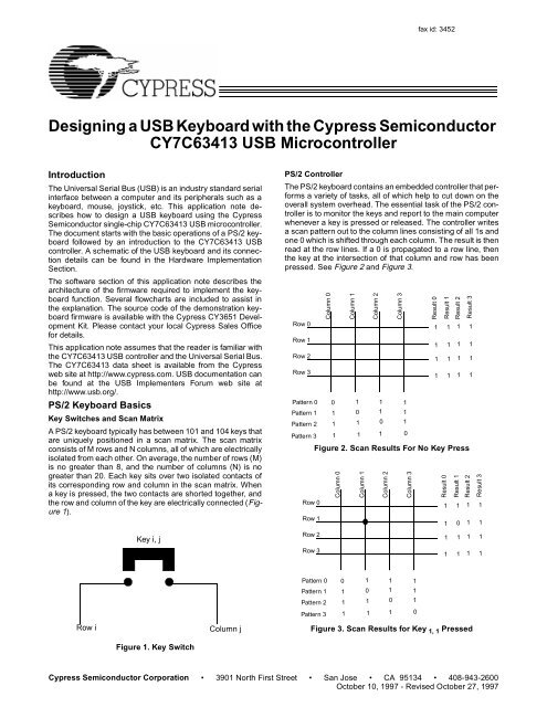
fax id: 3452<strong>Designing</strong> a <strong>USB</strong> <strong>Keyboard</strong> <strong>with</strong> <strong>the</strong> <strong>Cypress</strong> <strong>Semiconductor</strong>CY7C63413 <strong>USB</strong> MicrocontrollerIntroductionThe Universal Serial Bus (<strong>USB</strong>) is an industry standard serialinterface between a computer and its peripherals such as akeyboard, mouse, joystick, etc. This application note describeshow to design a <strong>USB</strong> keyboard using <strong>the</strong> <strong>Cypress</strong><strong>Semiconductor</strong> single-chip CY7C63413 <strong>USB</strong> microcontroller.The document starts <strong>with</strong> <strong>the</strong> basic operations of a PS/2 keyboardfollowed by an introduction to <strong>the</strong> CY7C63413 <strong>USB</strong>controller. A schematic of <strong>the</strong> <strong>USB</strong> keyboard and its connectiondetails can be found in <strong>the</strong> Hardware ImplementationSection.The software section of this application note describes <strong>the</strong>architecture of <strong>the</strong> firmware required to implement <strong>the</strong> keyboardfunction. Several flowcharts are included to assist in<strong>the</strong> explanation. The source code of <strong>the</strong> demonstration keyboardfirmware is available <strong>with</strong> <strong>the</strong> <strong>Cypress</strong> CY3651 DevelopmentKit. Please contact your local <strong>Cypress</strong> Sales Officefor details.This application note assumes that <strong>the</strong> reader is familiar <strong>with</strong><strong>the</strong> CY7C63413 <strong>USB</strong> controller and <strong>the</strong> Universal Serial Bus.The CY7C63413 data sheet is available from <strong>the</strong> <strong>Cypress</strong>web site at http://www.cypress.com. <strong>USB</strong> documentation canbe found at <strong>the</strong> <strong>USB</strong> Implementers Forum web site athttp://www.usb.org/.PS/2 <strong>Keyboard</strong> BasicsKey Switches and Scan MatrixA PS/2 keyboard typically has between 101 and 104 keys thatare uniquely positioned in a scan matrix. The scan matrixconsists of M rows and N columns, all of which are electricallyisolated from each o<strong>the</strong>r. On average, <strong>the</strong> number of rows (M)is no greater than 8, and <strong>the</strong> number of columns (N) is nogreater than 20. Each key sits over two isolated contacts ofits corresponding row and column in <strong>the</strong> scan matrix. Whena key is pressed, <strong>the</strong> two contacts are shorted toge<strong>the</strong>r, and<strong>the</strong> row and column of <strong>the</strong> key are electrically connected (Figure1).PS/2 ControllerThe PS/2 keyboard contains an embedded controller that performsa variety of tasks, all of which help to cut down on <strong>the</strong>overall system overhead. The essential task of <strong>the</strong> PS/2 controlleris to monitor <strong>the</strong> keys and report to <strong>the</strong> main computerwhenever a key is pressed or released. The controller writesa scan pattern out to <strong>the</strong> column lines consisting of all 1s andone 0 which is shifted through each column. The result is <strong>the</strong>nread at <strong>the</strong> row lines. If a 0 is propagated to a row line, <strong>the</strong>n<strong>the</strong> key at <strong>the</strong> intersection of that column and row has beenpressed. See Figure 2 and Figure 3.Row 0Row 1Row 2Row 3Pattern 0Pattern 1Pattern 2Pattern 3Row 0Row 1Column 0Column 10 11 01 11 1Column 2Column 31 11 10 11 0Result 0Result 1Result 2Result 3Figure 2. Scan Results For No Key PressColumn 0Column 1Column 2Column 31111111111111111Result 0Result 1Result 2Result 311101111Key i, jRow 21111Row 31111Pattern 0Pattern 1Pattern 2Pattern 30 11 01 11 11 11 10 11 0Row iColumn jFigure 3. Scan Results for Key 1, 1 PressedFigure 1. Key Switch<strong>Cypress</strong> <strong>Semiconductor</strong> Corporation • 3901 North First Street • San Jose • CA 95134 • 408-943-2600October 10, 1997 - Revised October 27, 1997
<strong>Designing</strong> a <strong>USB</strong> <strong>Keyboard</strong>PS/2 CableThe PS/2 keyboard is connected to <strong>the</strong> main computerthrough a shielded PS/2 cable that usually contains 6 wirescarrying 4 signals: Vcc, GND, Clock, and Data. The remaining2 wires are unused (one of <strong>the</strong>m is sometimes tied to chassisground.)Introduction to CY7C63413The CY7C63413 is a high performance 8-bit RISC microcontroller<strong>with</strong> an integrated <strong>USB</strong> Serial Interface Engine (SIE).The architecture implements 37 commands that are optimizedfor <strong>USB</strong> applications. The CY7C63413 has a built-inclock oscillator and timers, as well as general purpose I/Olines that can be configured as resistive <strong>with</strong> internal pull-ups,open-drain outputs, or traditional CMOS outputs. High performance,low-cost human-interface type computer peripheralssuch as a keypad or keyboard can be implemented <strong>with</strong> minimumexternal components and firmware effort.Clock CircuitThe CY7C63413 has a built-in clock oscillator and PLL-basedfrequency doubler. This circuit allows a cost effective 6 MHzceramic resonator to be used externally while <strong>the</strong> on-chipRISC core runs at 12 MHz.<strong>USB</strong> Serial Interface Engine (SIE)The operation of <strong>the</strong> SIE is totally transparent to <strong>the</strong> user. Inreceive mode, <strong>USB</strong> packet decode and data transfer to <strong>the</strong>endpoint FIFO are automatically done by <strong>the</strong> SIE. The SIE<strong>the</strong>n generates an interrupt to invoke <strong>the</strong> service routine aftera packet is unpacked.In <strong>the</strong> transmit mode, data transfer from <strong>the</strong> endpoint and <strong>the</strong>assembly of <strong>the</strong> <strong>USB</strong> packet are handled automatically by <strong>the</strong>SIE.General Purpose I/OThe CY7C63413 has 32 general purpose I/O lines dividedinto 4 ports: Port 0 through Port 3. One such I/O circuit isshown in Figure 4. Each port (8 bits) can be configured asresistive <strong>with</strong> internal pull-ups (7 KΩ), open drain outputs(high impedance inputs), or traditional CMOS outputs.Theport configuration is determined according to Table 1 below.Table 1. GPIO ConfigurationPortConfigurationBitsPinInterrupt Bit Driver ModeInterruptPolarity11 X Resistive -10 0 CMOS disabledOutput10 1 CMOS Input disabled01 X Open Drain -00 X Open Drain +Ports 0 to 2 offer low current drive <strong>with</strong> a typical current sinkcapability of 7 mA. Port 3 offers higher current drive, <strong>with</strong> atypical current sink of 12 mA which can be used to drive LEDs.Each General Purpose I/O (GPIO) is capable of generatingan interrupt to <strong>the</strong> RISC core. Interrupt polarity is selectableon a per port basis using <strong>the</strong> GPIO Configuration Register(see Table 1 above.) Selecting a negative polarity (“-”) willcause falling edges to trigger an interrupt, while a positivepolarity (“+”) selects rising edges as triggers. The interrupttriggered by a GPIO line is individually enabled by a dedicatedbit in <strong>the</strong> Interrupt Enable Register. All GPIO interrupts arefur<strong>the</strong>r masked by <strong>the</strong> Global GPIO Interrupt Enable Bit in <strong>the</strong>Global Interrupt Enable Register.The GPIO Configuration Register is located at I/O address0x08. The Data Registers are located at I/O addresses 0x00to 0x03 for Port 0 to Port 3 respectively.Power-up ModeThe CY7C63413 offers 2 modes of operation after a power-on-reset(POR) event: suspend-on-reset (typical for a <strong>USB</strong>application) and run-on-reset (typical for a PS/2 application).The suspend-on-reset mode is selected by attaching a pull-upresistor (100K to 470K Ω) to Vcc on Bit 7 of GPIO Port 3. Therun-on-reset mode is selected by attaching a pull-down resistor(0 to 470K Ω) to ground on Bit 7 of GPIO Port 3. See Figure5 and Figure 6.GPIOCFGmode2-bitsV CCInternalData BusInterruptEnableInternalBufferDataOutLatchPort WritePort ReadControl ControlQ17 KΩQ2to InterruptControllerQ3ESDGPIOPinFigure 4. One General Purpose I/O Line2
<strong>Designing</strong> a <strong>USB</strong> <strong>Keyboard</strong>Port 3, Bit 7VCCFigure 5. Suspend-On-Reset ModePort 3, Bit 7Figure 6. Run-On-Reset ModeHardware ImplementationRpullup100K100K toto470K470KΩOHMRpulldown0 toto470K470KΩOHMFigure 8 is <strong>the</strong> schematic for a keyboard application.Port 2 is configured as resistive (7 Kohm pull-ups to Vcc), andis connected to <strong>the</strong> M rows of <strong>the</strong> scan matrix (up to 8 rowsare supported). Port 0, 1, and 3 are also configured as resistive,and are connected to <strong>the</strong> N columns of <strong>the</strong> scan matrix(up to 20 columns are supported.) The 3 LEDs (Num Lock,Caps Lock, and Scroll Lock) are connected to <strong>the</strong> lower threebits of Port 3 as well (for high current drive.) For scan matrices<strong>with</strong> less than 8 rows or 20 columns, <strong>the</strong> unused port bitsshould be left unconnected (internally, <strong>the</strong>y are pulled up).During a scan test where no key is pressed, <strong>the</strong> row port databits will be high since all row lines are internally pulled up toVcc. When a key is pressed, setting its column port line lowwill cause its row line to go low as well. See Figure 7.Port 3, Bit 7 is pulled up to Vcc through a 470K Ω resistor (R5)so that <strong>the</strong> microcontroller will suspend after a POR. The microcontrollerwill resume once it detects bus activity (i.e <strong>USB</strong>Bus Reset).A 6 MHz ceramic resonator is connected to <strong>the</strong> clock inputsof <strong>the</strong> microcontroller. This component should be placed asclose to <strong>the</strong> microcontroller as possible.Since <strong>the</strong> keyboard is a bus-powered device, <strong>the</strong> 5V Vcc andGND come directly from <strong>the</strong> <strong>USB</strong> cable. The Vcc pin is connectedto <strong>the</strong> Vcc of <strong>the</strong> cable through a ramp regulating resistorof 1.5 Ω (R6). This resistor, along <strong>with</strong> a 22 µF capacitor(C2) connected between <strong>the</strong> Vcc and GND pins, provideroughly a 30 µs power ramp time. Vcc is also bypassed forhigh frequency noise by a 0.1 µF capacitor (C1).According to <strong>the</strong> <strong>USB</strong> specification, <strong>the</strong> <strong>USB</strong> D– line of alow-speed device (1.5 Mbps) should be tied to a voltagesource between 3.0V and 3.6V <strong>with</strong> a 1.5 KΩ pull-up terminator.The CY7C63413 eliminates <strong>the</strong> need for a 3.3V regulatorby specifying a 7.5 KΩ resistor (R1) connected between <strong>the</strong><strong>USB</strong> D– line and <strong>the</strong> nominal 5V Vcc.Row port lineVCCRow iVCCColumn port linColumn jFigure 7. Row/Column Port Configuration3
<strong>Designing</strong> a <strong>USB</strong> <strong>Keyboard</strong>Figure 8. Hardware Implementation4
<strong>Designing</strong> a <strong>USB</strong> <strong>Keyboard</strong>Firmware Implementation<strong>USB</strong> InterfaceAll <strong>USB</strong> Human Interface Device (HID) class applicationssuch as a keyboard, follow <strong>the</strong> same <strong>USB</strong> start-up procedure.The procedure is as follows (see Figure 9.)Device Plug-in(Power On Reset)Bus ResetEnumerationData Acquisition/TransferFigure 9. <strong>USB</strong> Start-Up ProcedureDevice Plug-in (Power On Reset)The <strong>USB</strong> device is powered when it is connected to <strong>the</strong> bus.The pull-up resistor on D– notifies <strong>the</strong> hub that a low-speed(1.5 Mbps) device has just been connected. Program executionbegins at address 0 (see Figure 10).ResetBus Reset• Enable device address 0• Enable 1ms Timer Interrupt• Enable End Point 0 to respond toSETUP packetsReturnFigure 11. Bus Reset ISREnumerationThe host sends a SETUP packet followed by IN packets toread <strong>the</strong> device description from default address 0. When <strong>the</strong>description is received, <strong>the</strong> host assigns a new <strong>USB</strong> addressto <strong>the</strong> device. The device begins responding to communication<strong>with</strong> <strong>the</strong> newly assigned address. The host <strong>the</strong>n asks for<strong>the</strong> device descriptor, configuration descriptor and HID reportdescriptor. The descriptors hold <strong>the</strong> information about <strong>the</strong> device.They will be discussed in detail below. Using <strong>the</strong> informationreturned from <strong>the</strong> device, <strong>the</strong> host now knows <strong>the</strong>number of data endpoints supported by <strong>the</strong> device (in a <strong>USB</strong>keyboard, <strong>the</strong>re is only one data endpoint). The host will issuea Set Configuration <strong>with</strong> a value of 1. At this point, <strong>the</strong> processof enumeration is completed. See Figures 12, 13, and 14.Perform InitializationEnable Bus Reset InterruptEnd Point 0Suspend until Bus Resetreceived aSETUP packetNWait for EnumerationYExecute main loop• Responds toSETUP packetaccording to <strong>the</strong>parsing structureBus ResetFigure 10. Power On ResetThe host recognizes <strong>the</strong> presence of a new <strong>USB</strong> device andresets it (see Figure 11).returnFigure 12. Endpoint 0 ISR5
<strong>Designing</strong> a <strong>USB</strong> <strong>Keyboard</strong>bmrequest typehost to devdev recip0x00host to devinter recip0x01host to devendp recip0x02dev to hostdev recip0x80dev to hostinter recip0x81dev to hostendp recip0x82get status0x00clr feature0x01set feature0x3set addr0x05get desc0x06set desc0x07get config0x08set config0x09get inter0x0Aset inter0x0Bsynch0x0CbrequestFigure 13. <strong>USB</strong> Standard Request Parsing Structurebmrequest typehost to devinter recip0x21dev to hostinter recip0xA1get_report0x01get_idle0x02get_protocol0x03set_report0x09set_idle0x0Aset_protocol0x0BbrequestFigure 14. <strong>USB</strong> HID Class Request Parsing StructureData Acquisition/TransferThe firmware periodically writes scan patterns to <strong>the</strong> scanmatrix columns, and reads <strong>the</strong> row result to determine whichkeys are pressed. The scan codes of <strong>the</strong> keys pressed aresent to <strong>the</strong> host using endpoint 1 (see Figure 15). When <strong>the</strong>host issues IN packets to retrieve data from <strong>the</strong> device, <strong>the</strong>device returns eight bytes of data. These eight bytes hold <strong>the</strong>keyboard control data (see Figure 16). Usage codes for eachkey can be found in Appendix A.3 of <strong>the</strong> Device Class Definitionfor Human Interface Devices (HID). When one of <strong>the</strong> LEDbuttons (i.e. Num Lock, Caps Lock, Scroll Lock) are pressedor released, <strong>the</strong> host issues a SETUP packet <strong>with</strong> aSet_Report request through <strong>the</strong> control pipe to End Point 0,followed by an OUT packet <strong>with</strong> 1 Data byte indicating whichLED should be on or off (see Figure 17.)6
<strong>Designing</strong> a <strong>USB</strong> <strong>Keyboard</strong>Figure 15. Endpoint 1 Interrupt Service RoutineByte 7 - Key 6Byte 6 - Key 5Byte 5 - Key 4Byte 4 - Key 3Byte 3 - Key 2Byte 2 - Key 1Byte 1 - ReservedBit 7 Bit 0RightGUIEnd Point 1RightAltReceivedACK fromlast TxYesRightShiftRightCtrlNoClear End Point 1 FIFOToggle Data PIDLeftGUILeftAltLeftShiftReturnLeftCtrlByte 0-ModifierFigure 16. IN Data Organization for <strong>USB</strong> <strong>Keyboard</strong>Bit 7 Bit 0ConstantConstantConstantKana ComposeScrollLockCapsLockNumLockByte 0-LED reportFigure 17. LED Report for <strong>USB</strong> <strong>Keyboard</strong>The byte order and bit field positions are defined by <strong>the</strong> HIDreport descriptor (discussed below), and are also consistent<strong>with</strong> <strong>the</strong> Boot Protocol requirements for legacy systems.<strong>USB</strong> DescriptorsAs stated earlier, <strong>the</strong> <strong>USB</strong> descriptors hold information about<strong>the</strong> device. There are several types of descriptors, which willbe discussed in detail below. All descriptors have certaincharacteristics in common. Byte 0 is always <strong>the</strong> descriptorlength in bytes and Byte 1 is always <strong>the</strong> descriptor type. Discussionof <strong>the</strong>se two bytes will be omitted from <strong>the</strong> followingdescriptions. The rest of <strong>the</strong> descriptor structure is dependenton <strong>the</strong> descriptor type. An example of each descriptor will begiven. Descriptor types are device, configuration, interface,endpoint, string, report, and several different class descriptors.Device DescriptorThis is <strong>the</strong> first descriptor <strong>the</strong> host requests from <strong>the</strong> device.It contains important information about <strong>the</strong> device. The sizeof this descriptor is 18 bytes. A list follows:• <strong>USB</strong> Specification release number in binary-coded decimal(BCD) (2 bytes)• Device class (1 byte)• Device subclass (1 byte)• Device protocol (1 byte)• Max packet size for Endpoint 0 (1 byte)• Vendor ID (2 bytes)• Product ID (2 bytes)• Device release number in BCD (2 bytes)• Index of string describing Manufacturer (Optional) (1 byte)• Index of string describing Product (Optional) (1 byte)• Index of string containing serial number (Optional) (1 byte)• Number of configurations for <strong>the</strong> device (1 byte)Example of a device descriptorDescriptor Length (18 bytes)Descriptor Type (Device)Complies to <strong>USB</strong> Spec Release (1.00)Class Code (insert code)Subclass Code (0)Protocol (No specific protocol)Max Packet Size for endpt 0 (8 bytes)Vendor ID (<strong>Cypress</strong>)Product ID (<strong>USB</strong> <strong>Keyboard</strong>)Device Release Number (1.03)String Describing Vendor (None)String Describing Product (None)String for Serial Number (None)Possible Configurations (1)7
<strong>Designing</strong> a <strong>USB</strong> <strong>Keyboard</strong>Configuration DescriptorThe configuration descriptor is 9 bytes in length and gives <strong>the</strong>configuration information for <strong>the</strong> device. It is possible to havemore than one configuration for each device. When <strong>the</strong> hostrequests a configuration descriptor, it will continue to read<strong>the</strong>se descriptors until all configurations have been received.A list of <strong>the</strong> structure follows:• Total length of <strong>the</strong> data returned for this configuration (2bytes)• Number of interfaces for this configuration (1 byte)• Value used to address this configuration (1 byte)• Index of string describing this configuration (Optional) (1byte)• Attributes bitmap describing configuration characteristics(1 byte)• Maximum power <strong>the</strong> device will consume from <strong>the</strong> bus (1byte)Example of configuration descriptorDescriptor Length (9 bytes)Descriptor Type (Configuration)Total Data Length (34 bytes)Interfaces Supported (1)Configuration Value (1)String Describing this Config (None)Config Attributes (Bus powered)Max Bus Power Consumption (100mA)Interface DescriptorThe interface descriptor is 9 bytes long and describes <strong>the</strong>interface of each device. It is possible to have more than oneinterface for each device. This descriptor is set up as follows:• Number of this interface (1 byte)• Value used to select alternate setting for this interface (1byte)• Number of endpoints used by this interface. If this numberis zero, only endpoint 0 is used by this interface (1 byte)• Class code (1 byte)• Subclass code (1 byte)• Protocol code (1 byte)• Index of string describing this interface (1 byte)Example of interface descriptorDescriptor Length (9 bytes)Descriptor Type (Interface)Interface Number (0)Alternate Setting (0)Number of Endpoints (1)Class Code (insert code)Subclass Code (0)Protocol (No specific protocol)String Describing Interface (None)HID (Class) DescriptorThe class descriptor tells <strong>the</strong> host about <strong>the</strong> class of <strong>the</strong> device.In this case, <strong>the</strong> device falls in <strong>the</strong> human interface device(HID) class. This descriptor is 9 bytes in length and is setup as follows:• Class release number in BCD (2 bytes)• Localized country code (1 byte)• Number of HID class descriptor to follow (1 byte)• Report descriptor type (1 byte)• Total length of report descriptor in bytes (2 bytes)Example of HID class descriptorDescriptor Length (9 bytes)Descriptor Type (HID Class)HID Class Release Number (1.00)Localized Country Code (USA)Number of Descriptors (1)Report Descriptor Type (HID)Report Descriptor Length (63 bytes)Endpoint DescriptorThe endpoint descriptor describes each endpoint, including<strong>the</strong> attributes and <strong>the</strong> address of each endpoint. It is possibleto have more than one endpoint for each interface. This descriptoris 7 bytes long and is set up as follows:• Endpoint address (1 byte)• Endpoint attributes. Describes transfer type (1 byte)• Maximum packet size this endpoint is capable of transferring(2 bytes)• Time interval at which this endpoint will be polled for data(1 byte)Example of endpoint descriptorDescriptor Length (7 bytes)Descriptor Type (Endpoint)Endpoint Address (IN, Endpoint 1)Attributes (Interrupt)Maximum Packet Size (8 bytes)Polling Interval (10 ms)Report DescriptorThis is <strong>the</strong> most complicated descriptor in <strong>USB</strong>. There is noset structure. It is more like a computer language that describes<strong>the</strong> format of <strong>the</strong> device’s data in detail. This descriptoris used to define <strong>the</strong> structure of <strong>the</strong> data returned to <strong>the</strong>host as well as to tell <strong>the</strong> host what to do <strong>with</strong> that data. Anexample of a report descriptor can be found below.A report descriptor must contain <strong>the</strong> following items: Input (orOutput or Feature), Usage, Usage Page, Logical Minimum,Logical Maximum, Report size, and Report Count. These areall necessary to describe <strong>the</strong> device’s data.Example of report descriptorUsage Page (Generic Desktop)Usage (<strong>Keyboard</strong>)Collection (Application)Usage Page(key codes)Usage Minimum (224)Usage Maximum (231)Logical Minimum (0)Logical Maximum (1)Report Size (1)Report Count (8) ; modifier byteInput (Data, Variable, Absolute)Report Count (1)Report Size (8)Input (Constant) ; reserved byte8
<strong>Designing</strong> a <strong>USB</strong> <strong>Keyboard</strong>Report Count (5)Report Size (1)Usage Page (LEDs)Usage Minimum (1)Usage Maximum (5)Output (Data, Variable,Absolute); LED reportReport Count (1)Report Size (3)Output (Constant) ;paddingReport Count (6)Report Size (8)Logical Minimum (0)Logical Maximum (101)Usage Page (key codes)Usage Minimum (0)Usage Maximum (101)Input (Data, Array) ;key array(6)End CollectionInput items are used to tell <strong>the</strong> host what type of data will bereturned as input to <strong>the</strong> host for interpretation. These itemsdescribe attributes such as data vs. constant, variable vs. array,absolute vs. relative, etc.Usages are <strong>the</strong> part of <strong>the</strong> descriptor that defines what shouldbe done <strong>with</strong> <strong>the</strong> data that is returned to <strong>the</strong> host. From <strong>the</strong>example descriptor, Usage (<strong>Keyboard</strong>) tells <strong>the</strong> host that thisis a keyboard device. There is also ano<strong>the</strong>r kind of Usage tagfound in <strong>the</strong> example called a Usage Page. The reason for <strong>the</strong>Usage Page is that it is necessary to allow for more than 256possible Usage tags. Usage Page tags are used as a secondbyte which allows for up to 65536 Usages.Logical Minimum and Logical Maximum are used to bound<strong>the</strong> values that a device will return. For example, a keyboardthat will return <strong>the</strong> values 0 to 101 for <strong>the</strong> scan code of eachkey press will have a Logical Minimum (0) and Logical Maximum(101). These are different from Physical Minimum andPhysical Maximum. Physical boundaries give some meaningto <strong>the</strong> Logical boundaries. For example, a <strong>the</strong>rmometer mayhave Logical boundaries of 0 to 999, but <strong>the</strong> Physical boundariesmay be 32 to 212. In o<strong>the</strong>r words, <strong>the</strong> boundaries on <strong>the</strong><strong>the</strong>rmometer are 32 to 212 degrees Fahrenheit, but <strong>the</strong>re areone thousand steps defined between <strong>the</strong> boundaries.Report Size and Report Count define <strong>the</strong> structures that <strong>the</strong>data will be transferred in. Report Size gives <strong>the</strong> size of <strong>the</strong>structure in bits. Report Count defines how many structureswill be used. In <strong>the</strong> example descriptor above, <strong>the</strong> lines ReportSize (8) and Report Count (6) define a 6 byte key arrayfor a keyboard.Collection items are used to show a relationship between twoor more sets of data. For example, a minimal keyboard canbe described as a collection of four data items (Modifier byte,Reserved byte, LED report, and Key Array). End Collectionitems simply close <strong>the</strong> collection.It is important to note that all examples given here are merelyfor clarification. They are not necessarily definitive solutions.A more detailed description of all items discussed here aswell as o<strong>the</strong>r descriptor issues can be found in <strong>the</strong> “DeviceClass Definition for Human Interface Devices (HID)” revision1.0 and in <strong>the</strong> “Universal Serial Bus Specification” revision1.0, chapter 9. Both of <strong>the</strong>se documents can be found on <strong>the</strong><strong>USB</strong> world wide web site at http://www.usb.org/.FunctionalityMain LoopThe main loop of <strong>the</strong> firmware (Figure 20) waits for <strong>the</strong> keyboardScan Task to be scheduled by <strong>the</strong> 1 ms ISR (Figure 25),and <strong>the</strong>n executes it. Reports are sent to <strong>the</strong> host via EndPoint 1 anytime a key is pressed or released. The host sidesoftware will repeat <strong>the</strong> key press until <strong>the</strong> release of <strong>the</strong> keyso that <strong>the</strong> device does not require a continuous report whenno key status changes have occurred.Scan TaskThe Scan Task (Figure 21) determines if <strong>the</strong>re were any keystatus changes from <strong>the</strong> previous scan (i.e. key presses orreleases) and calls <strong>the</strong> KeyChanged routine (Figure 22) foreach column of <strong>the</strong> scan matrix that had changes in any of<strong>the</strong> row positions. The KeyChanged routine calls <strong>the</strong>FoundKey routine (Figure 24) for each row that <strong>the</strong>re waschange in status. The FoundKey routine calculates an indexbased upon <strong>the</strong> row and column of <strong>the</strong> key, does a lookup ina KeyCodeTable for its usage (scan) code, and stores it in <strong>the</strong>End Point 1 FIFO. After all columns have been scanned, <strong>the</strong>Scan Task calls <strong>the</strong> SendKeys routine (Figure 23) if a reportis required to be sent to <strong>the</strong> host.DebounceThe mechanical switch properties of <strong>the</strong> key switches cause<strong>the</strong>m to bounce after a key press. These bounces may bemistaken for actual key events. See Figure 18.Row i SignalKey i, j pressedSwitch bouncesKey i, j releasedTimeFigure 18. Key Switch BounceTo solve this problem, all keys that are pressed have <strong>the</strong>ircode stored in a Debounce FIFO at <strong>the</strong> location pointed to by<strong>the</strong> Debounce Pointer (<strong>the</strong> reference firmware uses a 4-elementFIFO). The 1 ms ISR updates and clears <strong>the</strong> currentposition in <strong>the</strong> Debounce FIFO every 12 ms. Every key thathas a status change (i.e. pressed or released) is searched forin <strong>the</strong> Debounce FIFO. If <strong>the</strong> key is found, <strong>the</strong> status changeis ignored. In o<strong>the</strong>r words, any status change for 12*4= 48 msafter a key is pressed is considered to be caused by switchbounces, and should be disregarded. Different keyboards willhave varying key switch sensitivity, and <strong>the</strong> length of <strong>the</strong> DebounceFIFO may vary. The firmware uses <strong>the</strong> constantDEB_HI_ADDR to set <strong>the</strong> length of <strong>the</strong> FIFO.9
<strong>Designing</strong> a <strong>USB</strong> <strong>Keyboard</strong>Phantom KeysA phantom fourth key press (D) will be detected in a scanmatrix if two keys (A and B) in <strong>the</strong> same column are pressed,along <strong>with</strong> a third key (C) pressed in <strong>the</strong> same row as A or B(see Figure 19). If this situation is detected, all 6 key arraypositions in <strong>the</strong> End Point 1 FIFO (bytes 2–7) will be loaded<strong>with</strong> usage code 01h to report a Rollover error to <strong>the</strong> host.This tells <strong>the</strong> host that <strong>the</strong> firmware was unable to accuratelydetermine which key presses had occurred.Row 0Row 1Column 0Column 1D (phantom)Column 2Column 3BResult 0Result 1Result 2Result 310111110<strong>the</strong> key in that position of <strong>the</strong> scan matrix. Unused locationsshould be filled <strong>with</strong> 00H.The reference Key Code Table contains a unique locationnumber in each column/row intersection, beginning <strong>with</strong> 01Hfor Column 0, Row 0 up to A0H for Column 19, Row 7. Theselocation codes are useful for determining <strong>the</strong> mappings ofkeys to <strong>the</strong> scan matrix if appropriate documentation is notavailable. This is possible through <strong>the</strong> use of a <strong>USB</strong> bus analyzertool to record DATA packets sent to <strong>the</strong> host <strong>with</strong> eachkey press. The contents of <strong>the</strong> recorded DATA packet point toexactly one location in <strong>the</strong> reference Key Code Table. Thelocation number can <strong>the</strong>n be replaced <strong>with</strong> <strong>the</strong> actual usagecode of <strong>the</strong> key pressed. Usage codes for <strong>the</strong> <strong>USB</strong> keyboardcan be found in Appendix A.3 of revision 1.0 of <strong>the</strong> DeviceClass Definition for Human Interface Devices (HID).Row 21111Row 3CA0110Main LoopPattern 00 11 1Pattern 1Pattern 2Pattern 3111011101110Wait for Taskto be SCAN_TASKN-Key RolloverFigure 19. Phantom Key SituationIn <strong>the</strong> case where multiple keys are pressed and held down,only <strong>the</strong> last key pressed should be repeated. To accomplishthis, <strong>the</strong> last key press is stored in <strong>the</strong> LastTx buffer and issent again in a separate report to <strong>the</strong> host whenever a multiplekey report is sent. Once <strong>the</strong> same key is released, a reportnotifying it of <strong>the</strong> release is sent to <strong>the</strong> host (all 6 key arraypositions are filled <strong>with</strong> 0’s).Suspend/Resume/Remote WakeupAccording to <strong>the</strong> <strong>USB</strong> Specification 1.0, a device has to gointo suspend mode after 3 ms of no bus activity. The 1 ms ISRdetermines when this condition occurs (by reading <strong>the</strong> BusActivity bit, bit 3, of <strong>the</strong> <strong>USB</strong> Status and Control Register, 1Fh)and suspends <strong>the</strong> microcontroller. This is accomplished bysetting bit 0 (<strong>the</strong> Run bit) and bit 3 (Suspend bit) of <strong>the</strong> ProcessorStatus and Control Register (FFh). The microcontrollerwill resume operation if a GPIO interrupt occurs or busactivity resumes.Prior to suspending <strong>the</strong> microcontroller, <strong>the</strong> 1 ms ISR pullsdown all <strong>the</strong> column port lines and enables a falling edgeinterrupt on all Port 2 lines (Row port). If any key is pressedwhile in <strong>the</strong> suspended state, one of <strong>the</strong> row lines will bepulled low and trigger a GPIO interrupt. The GPIO ISR (Figure26) will send a resume signal (force a K state where D+is high and D- is low for 10ms) to wake up <strong>the</strong> host (remotewake up).Key Code TableThe Key Code Table found at <strong>the</strong> end of <strong>the</strong> keyboard firmwaremust be filled in uniquely for each keyboard. Each keyboardhas unique, proprietary key mappings to its scan matrix.Each location in <strong>the</strong> Key Code Table corresponds to acolumn/row intersection that must contain <strong>the</strong> usage code forPerformScan TaskFigure 20. Main Loop10
<strong>Designing</strong> a <strong>USB</strong> <strong>Keyboard</strong>Scan TaskKeyChangedColumn = 0Row = 0Write scan pattern totest Column(Ports 0, 1, 3)Row statuschanged?YesCall FoundKeyroutineRead row bits(Port 2)NoIncrement RowCompare row bits <strong>with</strong>KeySwitchImage[Column]YesRow < 8?Changesfound?YesCall KeyChangedroutineNoNoReturnStore row bits inKeySwitchImage[Column]Figure 22. KeyChanged RoutineTxRequired?NoYesCall SendKeysroutine(this may be calledagain to send <strong>the</strong>LastTx if multiplekeys were sent inone packet).SendKeysEnable response to IN packets<strong>with</strong> 8 data bytesSet TxRequiredflag to FalseWait for ACKIncrement ColumnRespond to IN packets<strong>with</strong> NAKYesColumn < 20?NoReturnFigure 23. SendKeys RoutineSet Task to NO_TASKDoneFigure 21. Scan Task11
<strong>Designing</strong> a <strong>USB</strong> <strong>Keyboard</strong>FoundKey1 ms ISRKey =KeyCodeTable[Column][Row]Clear Watchdog TimerCompare row bit <strong>with</strong>KeySwitchImage[Column][Row]3 ms ofbus inactivity?YesSave GPIO Portsettings. Write ‘0’ toColumn port bits.Key statusPressedReleasedNoKey is amodifier?Key inDebounceFIFO?NoYesNoEnable GPIO interrupts(falling edge) on Port 2Suspend until busactivity resumesYes Key ==LastTx?NoDisable GPIO interrupts.Restore port settings.YesPhantomkey situation?Yes1Set TxRequiredflag to TrueHas 4 mspast?YesSet Task to SCAN_TASKNoDebounce_FIFO[Debounce_Pointer]=KeyNoSet TxRequired flagto TrueKey is amodifier?YesSet TxRequiredflag to TrueSet ModifierByte in FIFOHas 12 mspast?YesIncrementDebounce_PointerNoNoLastTx = Key1Debounce_FIFO[Debounce_Pointer] =Illegal matrix indexEP1 FIFOfull?YesFill EP1 FIFO <strong>with</strong>01H (Rollover Error)NoAdd Key to EP1 FIFOReturnReturnFigure 24. FoundKey RoutineFigure 25. 1 ms ISR12
<strong>Designing</strong> a <strong>USB</strong> <strong>Keyboard</strong>GPIO ISRBus is stillidle?NoYesSend Remote Wakeup signalReturnConclusionFigure 26. GPIO ISRThe two main enabling factors of <strong>the</strong> proliferation of <strong>the</strong> <strong>USB</strong>devices are cost and functionality. The CY7C63413 meetsboth requirements by integrating <strong>the</strong> <strong>USB</strong> SIE and multi-functionI/Os <strong>with</strong> a <strong>USB</strong> optimized RISC core for a low price perpart.© <strong>Cypress</strong> <strong>Semiconductor</strong> Corporation, 1997. The information contained herein is subject to change <strong>with</strong>out notice. <strong>Cypress</strong> <strong>Semiconductor</strong> Corporation assumes no responsibility for <strong>the</strong> useof any circuitry o<strong>the</strong>r than circuitry embodied in a <strong>Cypress</strong> <strong>Semiconductor</strong> product. Nor does it convey or imply any license under patent or o<strong>the</strong>r rights. <strong>Cypress</strong> <strong>Semiconductor</strong> does not authorizeits products for use as critical components in life-support systems where a malfunction or failure may reasonably be expected to result in significant injury to <strong>the</strong> user. The inclusion of <strong>Cypress</strong><strong>Semiconductor</strong> products in life-support systems application implies that <strong>the</strong> manufacturer assumes all risk of such use and in doing so indemnifies <strong>Cypress</strong> <strong>Semiconductor</strong> against all charges.