Designing a USB Keyboard with the Cypress Semiconductor ...
Designing a USB Keyboard with the Cypress Semiconductor ...
Designing a USB Keyboard with the Cypress Semiconductor ...
- No tags were found...

Create successful ePaper yourself
Turn your PDF publications into a flip-book with our unique Google optimized e-Paper software.
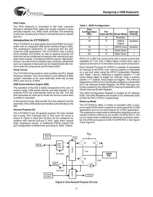
<strong>Designing</strong> a <strong>USB</strong> <strong>Keyboard</strong>PS/2 CableThe PS/2 keyboard is connected to <strong>the</strong> main computerthrough a shielded PS/2 cable that usually contains 6 wirescarrying 4 signals: Vcc, GND, Clock, and Data. The remaining2 wires are unused (one of <strong>the</strong>m is sometimes tied to chassisground.)Introduction to CY7C63413The CY7C63413 is a high performance 8-bit RISC microcontroller<strong>with</strong> an integrated <strong>USB</strong> Serial Interface Engine (SIE).The architecture implements 37 commands that are optimizedfor <strong>USB</strong> applications. The CY7C63413 has a built-inclock oscillator and timers, as well as general purpose I/Olines that can be configured as resistive <strong>with</strong> internal pull-ups,open-drain outputs, or traditional CMOS outputs. High performance,low-cost human-interface type computer peripheralssuch as a keypad or keyboard can be implemented <strong>with</strong> minimumexternal components and firmware effort.Clock CircuitThe CY7C63413 has a built-in clock oscillator and PLL-basedfrequency doubler. This circuit allows a cost effective 6 MHzceramic resonator to be used externally while <strong>the</strong> on-chipRISC core runs at 12 MHz.<strong>USB</strong> Serial Interface Engine (SIE)The operation of <strong>the</strong> SIE is totally transparent to <strong>the</strong> user. Inreceive mode, <strong>USB</strong> packet decode and data transfer to <strong>the</strong>endpoint FIFO are automatically done by <strong>the</strong> SIE. The SIE<strong>the</strong>n generates an interrupt to invoke <strong>the</strong> service routine aftera packet is unpacked.In <strong>the</strong> transmit mode, data transfer from <strong>the</strong> endpoint and <strong>the</strong>assembly of <strong>the</strong> <strong>USB</strong> packet are handled automatically by <strong>the</strong>SIE.General Purpose I/OThe CY7C63413 has 32 general purpose I/O lines dividedinto 4 ports: Port 0 through Port 3. One such I/O circuit isshown in Figure 4. Each port (8 bits) can be configured asresistive <strong>with</strong> internal pull-ups (7 KΩ), open drain outputs(high impedance inputs), or traditional CMOS outputs.Theport configuration is determined according to Table 1 below.Table 1. GPIO ConfigurationPortConfigurationBitsPinInterrupt Bit Driver ModeInterruptPolarity11 X Resistive -10 0 CMOS disabledOutput10 1 CMOS Input disabled01 X Open Drain -00 X Open Drain +Ports 0 to 2 offer low current drive <strong>with</strong> a typical current sinkcapability of 7 mA. Port 3 offers higher current drive, <strong>with</strong> atypical current sink of 12 mA which can be used to drive LEDs.Each General Purpose I/O (GPIO) is capable of generatingan interrupt to <strong>the</strong> RISC core. Interrupt polarity is selectableon a per port basis using <strong>the</strong> GPIO Configuration Register(see Table 1 above.) Selecting a negative polarity (“-”) willcause falling edges to trigger an interrupt, while a positivepolarity (“+”) selects rising edges as triggers. The interrupttriggered by a GPIO line is individually enabled by a dedicatedbit in <strong>the</strong> Interrupt Enable Register. All GPIO interrupts arefur<strong>the</strong>r masked by <strong>the</strong> Global GPIO Interrupt Enable Bit in <strong>the</strong>Global Interrupt Enable Register.The GPIO Configuration Register is located at I/O address0x08. The Data Registers are located at I/O addresses 0x00to 0x03 for Port 0 to Port 3 respectively.Power-up ModeThe CY7C63413 offers 2 modes of operation after a power-on-reset(POR) event: suspend-on-reset (typical for a <strong>USB</strong>application) and run-on-reset (typical for a PS/2 application).The suspend-on-reset mode is selected by attaching a pull-upresistor (100K to 470K Ω) to Vcc on Bit 7 of GPIO Port 3. Therun-on-reset mode is selected by attaching a pull-down resistor(0 to 470K Ω) to ground on Bit 7 of GPIO Port 3. See Figure5 and Figure 6.GPIOCFGmode2-bitsV CCInternalData BusInterruptEnableInternalBufferDataOutLatchPort WritePort ReadControl ControlQ17 KΩQ2to InterruptControllerQ3ESDGPIOPinFigure 4. One General Purpose I/O Line2