Designing a Low-Cost Analog USB Joystick with the Cypress ...
Designing a Low-Cost Analog USB Joystick with the Cypress ...
Designing a Low-Cost Analog USB Joystick with the Cypress ...

Create successful ePaper yourself
Turn your PDF publications into a flip-book with our unique Google optimized e-Paper software.
<strong>Designing</strong> a <strong>Low</strong>-<strong>Cost</strong> <strong>USB</strong> <strong>Joystick</strong><br />
V CC<br />
Port Pull-Up<br />
Register<br />
Port Data<br />
Register<br />
Schmitt<br />
Trigger<br />
16 KΩ<br />
GPIO<br />
Pin<br />
Data Bus<br />
Port Isink<br />
Register<br />
Isink<br />
DAC<br />
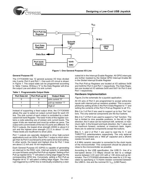
Figure 1. One General Purpose I/O Line<br />
General Purpose I/O<br />
The CY7C63000 has 12 general purpose I/O lines divided<br />
into 2 ports: Port 0 and Port 1. One such I/O circuit is shown<br />
in Figure 1. The output state can be programmed according<br />
to Table 1 below. Writing a “0” to <strong>the</strong> Data Register will drive<br />
<strong>the</strong> output <strong>Low</strong> and allow it to sink current.<br />
Table 1. Programmable Output State<br />
Port Data bit Port Pull-up bit Output State<br />
0 X sink current “0”<br />
1 0 pull-up resistor “1”<br />
1 1 High-Z<br />
Instead of supporting a fixed output drive, <strong>the</strong> CY7C63000<br />
allows <strong>the</strong> user to select an output current level for each I/O<br />
line. The sink current of each output is controlled by a dedicated<br />
8-bit Isink Register. The lower 4-bits of this register contains<br />
a code selecting one of sixteen sink current levels. The<br />
upper 4-bits are reserved and must be written as zeros. The<br />
output sink current levels of <strong>the</strong> two I/O ports are different. For<br />
Port 0 outputs, <strong>the</strong> lowest drive strength (0000) is about 0.2<br />
mA and <strong>the</strong> highest drive strength (1111) is about 1.0 mA.<br />
These levels are insufficient to drive LEDs.<br />
Port 1 outputs are specially designed to drive high-current<br />
applications such as LEDs. Each Port 1 output is much stronger<br />
than its Port 0 counterparts at <strong>the</strong> same drive level setting.<br />
In o<strong>the</strong>r words, <strong>the</strong> lowest and highest drive for Port 1 lines<br />
are about 3.2 mA and 16 mA respectively.<br />
Each General Purpose I/O (GPIO) is capable of generating<br />
an interrupt to <strong>the</strong> RISC core. Interrupt polarity is selectable<br />
on a per bit basis using <strong>the</strong> Port Pull-up register. Setting a Port<br />
Pull-up register bit to “1” will select a rising edge trigger for <strong>the</strong><br />
corresponding GPIO line. Conversely, setting a Port Pull-up<br />
Register bit to “0” will select a falling edge trigger. The interrupt<br />
triggered by a GPIO line is individually enabled by a dedicated<br />
bit in <strong>the</strong> Interrupt Enable Register. All GPIO interrupts<br />
are fur<strong>the</strong>r masked by <strong>the</strong> Global GPIO Interrupt Enable Bit<br />
in <strong>the</strong> Global Interrupt Enable Register<br />
The Port Pull-up Registers are located at I/O address 0x08<br />
and 0x09 for Port 0 and Port 1 respectively. The Data Registers<br />
are located at I/O address 0x00 and 0x01 for Port 0 and<br />
Port 1 respectively.<br />
Hardware Implementation<br />
Figure 2 is <strong>the</strong> schematic for a joystick application.<br />
All I/O pins of Port 0 are programmed to accept active-low<br />
inputs <strong>with</strong> internal pull-up resistors enabled. This is accomplished<br />
by setting all bits in <strong>the</strong> Port 0 Data Register to “1” and<br />
setting <strong>the</strong> contents of <strong>the</strong> Port 0 Pull-up Register to all “0”s.<br />
Bits 0 to 3 of Port 0 are used to support up to four “fire” buttons.<br />
The only external components are <strong>the</strong> four buttons.<br />
Bits 4 to 7 of Port 0 are used to support a “hat” function. The<br />
hat is limited to nine possible positions. In <strong>the</strong> left to right<br />
direction, <strong>the</strong> X value can be maximum left, centered, or maximum<br />
right. In <strong>the</strong> forward and back direction, <strong>the</strong> Y value can<br />
be maximum forward, centered, or maximum back. Again,<br />
<strong>the</strong>re are no external components except <strong>the</strong> buttons.<br />
Bits 0, 1, and 2 of Port 1 are used to read <strong>the</strong> X, Y, and<br />
THROTTLE potentiometers respectively. The only external<br />
components needed are a 1800 pF capacitor and a 2Kohm<br />
resistor for each axis.<br />
A 6 MHz ceramic resonator is connected to <strong>the</strong> clock inputs<br />
of <strong>the</strong> microcontroller. This component should be placed as<br />
close to <strong>the</strong> microcontroller as possible.<br />
According to <strong>the</strong> <strong>USB</strong> specification, <strong>the</strong> <strong>USB</strong> D– line of a<br />
low-speed device (1.5 Mbps) should be tied to a voltage<br />
source between 3.0V and 3.6V <strong>with</strong> a 1.5K ohms pull-up terminator.<br />
The CY7C63000 eliminates <strong>the</strong> need for a 3.3V regulator<br />
by specifying a 7.5 Kohm resistor connected between<br />
<strong>the</strong> <strong>USB</strong> D– line and <strong>the</strong> nominal 5V V CC (<strong>USB</strong> Power).<br />
2