Designing a Low-Cost USB Mouse with the Cypress Semiconductor ...
Designing a Low-Cost USB Mouse with the Cypress Semiconductor ...
Designing a Low-Cost USB Mouse with the Cypress Semiconductor ...

Create successful ePaper yourself
Turn your PDF publications into a flip-book with our unique Google optimized e-Paper software.
fax id: 3450<br />
<strong>Designing</strong> a <strong>Low</strong>-<strong>Cost</strong> <strong>USB</strong> <strong>Mouse</strong> <strong>with</strong> <strong>the</strong> <strong>Cypress</strong><br />
<strong>Semiconductor</strong> CY7C63000 <strong>USB</strong> Controller<br />
Introduction<br />
The Universal Serial Bus (<strong>USB</strong>) is an industrial standard serial<br />
interface between a computer and peripherals such as a<br />
mouse, joystick, keyboard, etc. This application note describes<br />
how a cost-effective <strong>USB</strong> opto-mechanical mouse<br />
can be built quickly using <strong>the</strong> <strong>Cypress</strong> <strong>Semiconductor</strong> single-chip<br />
CY7C63000 <strong>USB</strong> controller. The document starts<br />
<strong>with</strong> <strong>the</strong> basic operations of an opto-mechanical mouse followed<br />
by an introduction to <strong>the</strong> CY7C63000 <strong>USB</strong> controller.<br />
A schematic of <strong>the</strong> <strong>USB</strong> mouse and its connection details can<br />
be found in <strong>the</strong> Hardware Implementation Section.<br />
The software section of this application note describes <strong>the</strong><br />
architecture of <strong>the</strong> firmware required to implement <strong>the</strong> mouse<br />
function. Several sample code segments are included to assist<br />
in <strong>the</strong> explanation. The binary code of <strong>the</strong> complete<br />
mouse firmware is available free of charge from <strong>Cypress</strong><br />
<strong>Semiconductor</strong>. Please contact your local <strong>Cypress</strong> sales office<br />
for details.<br />
This application note assumes that <strong>the</strong> reader is familiar <strong>with</strong><br />
<strong>the</strong> CY7C63000 <strong>USB</strong> controller and <strong>the</strong> Universal Serial Bus.<br />
The CY7C63000 data sheet is available from <strong>the</strong> <strong>Cypress</strong><br />
web site at www.cypress.com. <strong>USB</strong> documentation can be<br />
found at <strong>the</strong> <strong>USB</strong> Implementers Forum web site at<br />
www.usb.org.<br />
<strong>USB</strong> <strong>Mouse</strong> Basics<br />
<strong>USB</strong> has been gaining popularity due to it’s simple connection,<br />
plug and play feature, and hot insertion capability. There<br />
are several kinds of <strong>USB</strong> pointing devices available in <strong>the</strong><br />
market. The opto-mechanical mouse is <strong>the</strong> most popular type<br />
because it provides relatively high resolution and works on a<br />
wide range of surfaces.<br />
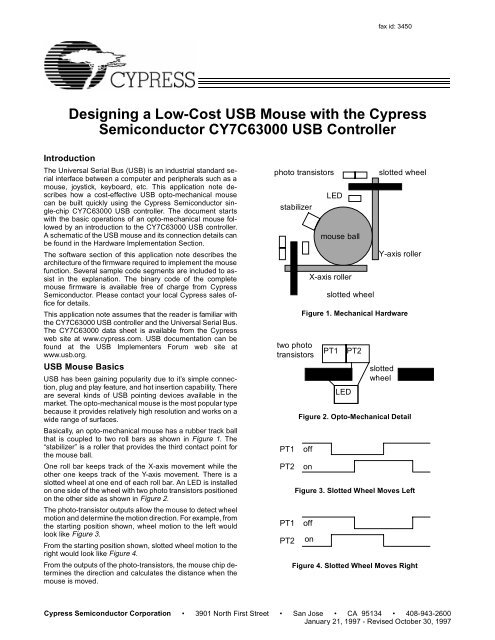
Basically, an opto-mechanical mouse has a rubber track ball<br />
that is coupled to two roll bars as shown in Figure 1. The<br />
“stabilizer” is a roller that provides <strong>the</strong> third contact point for<br />
<strong>the</strong> mouse ball.<br />
One roll bar keeps track of <strong>the</strong> X-axis movement while <strong>the</strong><br />
o<strong>the</strong>r one keeps track of <strong>the</strong> Y-axis movement. There is a<br />
slotted wheel at one end of each roll bar. An LED is installed<br />
on one side of <strong>the</strong> wheel <strong>with</strong> two photo transistors positioned<br />
on <strong>the</strong> o<strong>the</strong>r side as shown in Figure 2.<br />
The photo-transistor outputs allow <strong>the</strong> mouse to detect wheel<br />
motion and determine <strong>the</strong> motion direction. For example, from<br />
<strong>the</strong> starting position shown, wheel motion to <strong>the</strong> left would<br />
look like Figure 3.<br />
From <strong>the</strong> starting position shown, slotted wheel motion to <strong>the</strong><br />
right would look like Figure 4.<br />
From <strong>the</strong> outputs of <strong>the</strong> photo-transistors, <strong>the</strong> mouse chip determines<br />
<strong>the</strong> direction and calculates <strong>the</strong> distance when <strong>the</strong><br />
mouse is moved.<br />
photo transistors<br />
stabilizer<br />
two photo<br />
transistors<br />
PT1<br />
PT2<br />
PT1<br />
PT2<br />
LED<br />
mouse ball<br />
X-axis roller<br />
slotted wheel<br />
slotted wheel<br />
Y-axis roller<br />
Figure 1. Mechanical Hardware<br />
PT1<br />
LED<br />
PT2<br />
slotted<br />
wheel<br />
Figure 2. Opto-Mechanical Detail<br />
off<br />
on<br />
Figure 3. Slotted Wheel Moves Left<br />
off<br />
on<br />
Figure 4. Slotted Wheel Moves Right<br />
<strong>Cypress</strong> <strong>Semiconductor</strong> Corporation • 3901 North First Street • San Jose • CA 95134 • 408-943-2600<br />
January 21, 1997 - Revised October 30, 1997
<strong>Designing</strong> a <strong>Low</strong>-<strong>Cost</strong> <strong>USB</strong> <strong>Mouse</strong><br />
The resolution is <strong>the</strong> smallest motion <strong>the</strong> mouse can detect,<br />
measured in dots per inch (DPI). A typical opto-mechanical<br />
mouse has a resolution in <strong>the</strong> 200 to 400 DPI range. The<br />
mechanical dimensions of <strong>the</strong> mouse hardware limit <strong>the</strong> maximum<br />
achievable resolution.<br />
<strong>USB</strong> provides <strong>the</strong> plug-and-play feature that is not supported<br />
in RS-232 and PS/2 interfaces. The <strong>USB</strong> interface uses a<br />
four-pin connector <strong>with</strong> positive retention. A 28 AWG twisted<br />
pair is used for differential signaling and two 20 to 30 AWG<br />
wires are used to supply power and ground. No cable shielding<br />
is necessary for a mouse application.<br />
Introduction to CY7C63000<br />
The CY7C63000 is a high performance 8-bit RISC microcontroller<br />
<strong>with</strong> an integrated <strong>USB</strong> Serial Interface Engine (SIE).<br />
The architecture implements 34 commands that are optimized<br />
for <strong>USB</strong> applications. The CY7C63000 has built-in<br />
clock oscillator and timers as well as programmable current<br />
drivers, and pull-up resistors at each I/O line. High performance,<br />
low-cost human-interface type computer peripherals<br />
such as mouse, joystick, and gamepad can be implemented<br />
<strong>with</strong> minimum external components and firmware effort.<br />
Clock Circuit<br />
The CY7C63000 has a built-in clock oscillator and PLL-based<br />
frequency doubler. This circuit allows a cost effective 6 MHz<br />
ceramic resonator to be used externally while <strong>the</strong> on-chip<br />
RISC core runs at 12 MHz.<br />
<strong>USB</strong> Serial Interface Engine (SIE)<br />
The operation of <strong>the</strong> SIE is totally transparent to <strong>the</strong> user. In<br />
<strong>the</strong> receive mode, <strong>USB</strong> packet decode and data transfer to<br />
<strong>the</strong> endpoint FIFO are automatically done by <strong>the</strong> SIE. The SIE<br />
<strong>the</strong>n generates an interrupt request to invoke <strong>the</strong> service routine<br />
after a packet is unpacked.<br />
In <strong>the</strong> transmit mode, data transfer from <strong>the</strong> endpoint and <strong>the</strong><br />
assembly of <strong>the</strong> <strong>USB</strong> packet are handled automatically by <strong>the</strong><br />
SIE.<br />
General Purpose I/O<br />
The CY7C63000 has 12 general purpose I/O lines divided<br />
into 2 ports: Port 0 and Port 1. One such I/O circuit is shown<br />
in Figure 5. The output state can be programmed according<br />
to Table 1 below. Writing a “0” to <strong>the</strong> Data Register will drive<br />
<strong>the</strong> output <strong>Low</strong> and allow it to sink current.<br />
Table 1. Programmable Output State<br />
Port Data bit Port Pull-up bit Output State<br />
0 X sink current “0”<br />
1 0 pull-up resistor “1”<br />
1 1 High-Z<br />
Instead of supporting a fixed output drive, <strong>the</strong> CY7C63000<br />
allows <strong>the</strong> user to select an output current level for each I/O<br />
line. The sink current of each output is controlled by a dedicated<br />
8-bit Isink Register. The lower 4-bits of this register contains<br />
a code selecting one of sixteen sink current levels. The<br />
upper 4-bits are reserved and must be written as zeros. The<br />
output sink current levels of <strong>the</strong> two I/O ports are different. For<br />
Port 0 outputs, <strong>the</strong> lowest drive strength (0000) is about 0.2<br />
mA and <strong>the</strong> highest drive strength (1111) is about 1.0 mA.<br />
These levels are insufficient to drive <strong>the</strong> LEDs in a mouse.<br />
Port 1 outputs are specially designed to drive high-current<br />
applications such as LEDs. Each Port 1 output is much stronger<br />
than <strong>the</strong>ir Port 0 counterparts at <strong>the</strong> same drive level setting.<br />
In o<strong>the</strong>r words, <strong>the</strong> lowest and highest drive for Port 1<br />
lines are 3.2 mA and 16 mA respectively.<br />
Each General Purpose I/O (GPIO) is capable of generating<br />
an interrupt to <strong>the</strong> RISC core. Interrupt polarity is selectable<br />
on a per bit basis using <strong>the</strong> Port Pull-up register. Setting a Port<br />
Pull-up register bit to “1” will select a rising edge trigger for <strong>the</strong><br />
corresponding GPIO line. Conversely, setting a Port Pull-up<br />
Register bit to “0” will select a falling edge trigger. The interrupt<br />
triggered by a GPIO line is individually enabled by a dedicated<br />
bit in <strong>the</strong> Port Interrupt Enable Registers. All GPIO interrupts<br />
are fur<strong>the</strong>r masked by <strong>the</strong> Global GPIO Interrupt<br />
Enable Bit in <strong>the</strong> Global Interrupt Enable Register.<br />
V CC<br />
Port Pull-Up<br />
Register<br />
Port Data<br />
Register<br />
Schmitt<br />
Trigger<br />
16 KΩ<br />
GPIO<br />
Pin<br />
Data Bus<br />
Port Isink<br />
Register<br />
Isink<br />
DAC<br />
Figure 5. One General Purpose I/O Line<br />
2
<strong>Designing</strong> a <strong>Low</strong>-<strong>Cost</strong> <strong>USB</strong> <strong>Mouse</strong><br />
The Port Pull-up Registers are located at I/O address 0x08<br />
and 0x09 for Port 0 and Port 1 respectively. The Data Registers<br />
are located at I/O address 0x00 and 0x01 for Port 0 and<br />
Port 1 respectively. The Port 0 and Port 1 Interrupt Enable<br />
Registers are at addresses 0x04 and 0x05 respectively.<br />
Wake-Up Interrupt<br />
Power management is paramount in many <strong>USB</strong> applications.<br />
To conserve power, <strong>the</strong> CY7C63000 supports an externally<br />
programmable interrupt input to wake up <strong>the</strong> microcontroller<br />
from <strong>the</strong> suspend mode when <strong>the</strong> mouse is moved or when a<br />
button is pressed. The suspend mode causes <strong>the</strong> microcontroller<br />
to shut down most of its functions such as <strong>the</strong> clock<br />
circuit, <strong>the</strong> RISC core, <strong>the</strong> timer, and part of <strong>the</strong> SIE. In <strong>the</strong><br />
mouse application, a high percentage of <strong>the</strong> power is consumed<br />
by <strong>the</strong> LEDs. Therefore, <strong>the</strong> CY7C63000 should be<br />
programmed to turn off <strong>the</strong> LEDs before entering <strong>the</strong> suspend<br />
mode. With <strong>the</strong> LEDs off, <strong>the</strong> CY7C63000 can no longer detect<br />
any mouse movements although button closures are still<br />
recognized (because pressing a button causes an interrupt).<br />
This problem can be solved by using <strong>the</strong> wake-up interrupt<br />
that wakes up <strong>the</strong> microcontroller, checks for mouse movement,<br />
and <strong>the</strong>n goes back to suspend mode.<br />
The wake-up interrupt can be implemented by connecting <strong>the</strong><br />
CEXT pin to VCC <strong>with</strong> a resistor and to GND <strong>with</strong> a capacitor.<br />
Before <strong>the</strong> firmware puts <strong>the</strong> microcontroller into <strong>the</strong> suspend<br />
mode, it writes a zero to <strong>the</strong> Cext register at address 0x22 to<br />
discharge <strong>the</strong> external capacitor. Then, to start timing a one<br />
is written to <strong>the</strong> Cext register to allow <strong>the</strong> RC circuit to begin<br />
charging. A wake-up interrupt is generated to <strong>the</strong> RISC core<br />
when <strong>the</strong> external capacitor is charged up to nominal 2.75V<br />
(45% to 65% of Vcc) by <strong>the</strong> external resistor. The duration<br />
between successive wake-ups is controlled by <strong>the</strong> RC constant<br />
of <strong>the</strong> external resistor and capacitor.<br />
Hardware Implementation<br />
Figure 6 is <strong>the</strong> schematic for a mouse application.<br />
Photo transistor pins of Port 0 are programmed by writing a<br />
zero to <strong>the</strong> Data Registers which drives <strong>the</strong> output low. Then<br />
set <strong>the</strong> value of <strong>the</strong> Port Isink Register to <strong>the</strong> sink current<br />
value. One of sixteen sink current values could be selected.<br />
This is done to bias <strong>the</strong> photo transistors for correct operation.<br />
Button pins of Port 0 are programmed to accept active-low<br />
inputs <strong>with</strong> internal pull-up resistors enabled. This is accomplished<br />
by setting all bits in <strong>the</strong> Port 0 Data Register to “1” and<br />
setting <strong>the</strong> contents of <strong>the</strong> Port 0 Pull-up Register to all “0”s.<br />
Bits 4 to 6 of Port 0 are connected to <strong>the</strong> left, right, and middle<br />
buttons respectively. Bits 0 and 1 are connected to <strong>the</strong> left and<br />
right photo transistors of <strong>the</strong> horizontal axis respectively. Bits<br />
2 and 3 are connected to left and right photo transistors of <strong>the</strong><br />
vertical axis respectively.<br />
The two LEDs are connected in series to bit 0 of Port 1. The<br />
LEDs are turned off in <strong>the</strong> suspend mode to conserve power.<br />
The LEDs are switched on only when <strong>the</strong> mouse wakes up.<br />
Because <strong>the</strong> sink current of each GPIO line can be set to one<br />
of sixteen levels, <strong>the</strong> user can adjust <strong>the</strong> light output of <strong>the</strong><br />
LEDs to match <strong>the</strong> sensitivity of a wide range of photo transistors.<br />
The CEXT pin of <strong>the</strong> CY7C63000 is connected to an external<br />
RC timing circuit formed by R2 and C1. The wake-up time is<br />
set to about 20 msec to achieve a good balance between<br />
wake-up response time and power savings.<br />
A 6 MHz ceramic resonator is connected to <strong>the</strong> clock inputs<br />
of <strong>the</strong> microcontroller. This component should be placed as<br />
close to <strong>the</strong> microcontroller as possible.<br />
According to <strong>the</strong> <strong>USB</strong> specification, <strong>the</strong> <strong>USB</strong> D– line of a<br />
low-speed device (1.5 Mbps) should be tied to a voltage<br />
source between 3.0V and 3.6V <strong>with</strong> a 1.5K ohms pull-up terminator.<br />
The CY7C63000 eliminates <strong>the</strong> need for a 3.3V regulator<br />
by specifying a 7.5 Kohm resistor connected between<br />
<strong>the</strong> <strong>USB</strong> D– line and <strong>the</strong> nominal 5V Vcc.<br />
3
<strong>Designing</strong> a <strong>Low</strong>-<strong>Cost</strong> <strong>USB</strong> <strong>Mouse</strong><br />
Figure 6. Hardware Implementation<br />
4
<strong>Designing</strong> a <strong>Low</strong>-<strong>Cost</strong> <strong>USB</strong> <strong>Mouse</strong><br />
Firmware Implementation<br />
<strong>USB</strong> Interface<br />
All <strong>USB</strong> Human Interface Device (HID) class applications<br />
such as a mouse, follow <strong>the</strong> same <strong>USB</strong> start-up procedure.<br />
The procedure is as follows (see Figure 7):<br />
Device Plug-in<br />
Start<br />
• Set up stack pointer<br />
• Enable all interrupts being used<br />
Bus Reset<br />
Main Loop<br />
Enumeration<br />
Figure 8. Reset Interrupt Service Routine<br />
Data Acquisition/<br />
Transfer<br />
Figure 7. <strong>USB</strong> Start-Up Procedure<br />
End Point 0<br />
Device Plug-in<br />
When a <strong>USB</strong> device is first connected to <strong>the</strong> bus, it is powered<br />
but remains non-functional waiting for a bus reset. The pull-up<br />
resistor on D– notifies <strong>the</strong> hub that a low-speed (1.5 Mbps)<br />
device has just been connected.<br />
Bus Reset<br />
The host recognizes <strong>the</strong> presence of a new <strong>USB</strong> device and<br />
resets it (see Figure 8).<br />
Enumeration<br />
The host sends a SETUP packet followed by IN packets to<br />
read <strong>the</strong> device description from default address 0. When <strong>the</strong><br />
description is received, <strong>the</strong> host assigns a new <strong>USB</strong> address<br />
to <strong>the</strong> device. The device begins responding to communication<br />
<strong>with</strong> <strong>the</strong> newly assigned address, while <strong>the</strong> host continues<br />
to ask for information about <strong>the</strong> device description, configuration<br />
description and HID report description. Using <strong>the</strong><br />
information returned from <strong>the</strong> device, <strong>the</strong> host now knows <strong>the</strong><br />
number of data endpoints supported by <strong>the</strong> device (in a <strong>USB</strong><br />
mouse, <strong>the</strong>re is only one data endpoint). At this point, <strong>the</strong><br />
process of enumeration is completed. See Figures 9, 10 and<br />
11.<br />
received a<br />
SETUP packet<br />
• Responds to<br />
SETUP packet<br />
according to <strong>the</strong><br />
parsing structure<br />
return<br />
Y<br />
N<br />
Figure 9. Endpoint 0 ISR<br />
5
<strong>Designing</strong> a <strong>Low</strong>-<strong>Cost</strong> <strong>USB</strong> <strong>Mouse</strong><br />
bmrequest type<br />
host to dev<br />
dev recip<br />
0x00<br />
host to dev<br />
inter recip<br />
0x01<br />
host to dev<br />
endp recip<br />
0x02<br />
dev to host<br />
dev recip<br />
0x80<br />
dev to host<br />
inter recip<br />
0x81<br />
dev to host<br />
endp recip<br />
0x82<br />
get status<br />
0x00<br />
clr feature<br />
0x01<br />
set feature<br />
0x3<br />
set addr<br />
0x05<br />
get desc<br />
0x06<br />
set desc<br />
0x07<br />
get config<br />
0x08<br />
set config<br />
0x09<br />
get inter<br />
0x0A<br />
set inter<br />
0x0B<br />
synch<br />
0x0C<br />
brequest<br />
Figure 10. <strong>USB</strong> Standard Request Parsing Structure<br />
bmrequest type<br />
host to dev<br />
inter recip<br />
0x21<br />
dev to host<br />
inter recip<br />
0xA1<br />
get_reportl<br />
0x01<br />
get_idle<br />
0x02<br />
get_protocol<br />
0x03<br />
set_reportl<br />
0x09<br />
set_idle<br />
0x0A<br />
set_protocol<br />
0x0B<br />
brequest<br />
Figure 11. <strong>USB</strong> HID Class Request Parsing Structure<br />
Data Acquisition/Transfer<br />
The firmware polls <strong>the</strong> mouse buttons and <strong>the</strong> photo transistors.<br />
The status of <strong>the</strong> buttons as well as <strong>the</strong> horizontal and<br />
vertical displacements are sent to <strong>the</strong> host using endpoint 1.<br />
When <strong>the</strong> host issues IN packets to retrieve data from <strong>the</strong><br />
device, <strong>the</strong> device returns three bytes of data as shown in<br />
Figure 12. Figure 13 illustrates response to an e14, and 15.)<br />
Bit 7 Bit 0<br />
N/A N/A N/A N/A N/A Mid Right Left Byte 0 - buttons<br />
Bit 7 Bit 0<br />
HD7 HD6 HD5 HD4 HD3 HD2 HD1 HD0 Byte 1 - Horizontal<br />
displacement<br />
Bit 7 Bit 0<br />
VD7 VD6 VD5 VD4 VD3 VD2 VD1 VD0 Byte 2 - Vertical<br />
displacement<br />
Figure 12. Data Organization for <strong>USB</strong> <strong>Mouse</strong><br />
6
<strong>Designing</strong> a <strong>Low</strong>-<strong>Cost</strong> <strong>USB</strong> <strong>Mouse</strong><br />
Endpoint_1<br />
• Prepare data in Endpoint_1 DMA<br />
buffer<br />
• Re-enable interrupts<br />
Return<br />
Figure 13. Endpoint 1 Interrupt Service Routine<br />
lh = left horizontal photo transistor<br />
rh = right horizontal photo transistor<br />
r/l = right / left bit state<br />
r/l=0 0<br />
lh=0<br />
STATE 0<br />
rh=0<br />
r/l=01<br />
STATE 1<br />
rh=01<br />
lh=1 rh=1<br />
rh=10 lh=10<br />
STATE 3<br />
lh=01<br />
STATE 2<br />
r/l=10<br />
r/l=11<br />
Figure 14. <strong>Mouse</strong> State Diagram<br />
State 3 State 2 State 0 State 1 State 3<br />
Left horizontal<br />
photo transistor output<br />
Right horizontal<br />
photo transistor output<br />
Left movement Right movement<br />
Figure 15. State Definitions<br />
7
<strong>Designing</strong> a <strong>Low</strong>-<strong>Cost</strong> <strong>USB</strong> <strong>Mouse</strong><br />
The byte order and bit field positions are defined by <strong>the</strong> <strong>USB</strong><br />
HID specification.<br />
<strong>USB</strong> Descriptors<br />
As stated earlier, <strong>the</strong> <strong>USB</strong> descriptors hold information about<br />
<strong>the</strong> device. There are several types of descriptors, which will<br />
be discussed in detail below. All descriptors have certain<br />
characteristics in common. Byte 0 is always <strong>the</strong> descriptor<br />
length in bytes and Byte 1 is always <strong>the</strong> descriptor type. Discussion<br />
of <strong>the</strong>se two bytes will be omitted from <strong>the</strong> following<br />
descriptions. The rest of <strong>the</strong> descriptor structure is dependent<br />
on <strong>the</strong> descriptor type. An example of each descriptor will be<br />
given. Descriptor types are device, configuration, interface,<br />
endpoint, string, report, and several different class descriptors.<br />
Device Descriptor<br />
This is <strong>the</strong> first descriptor <strong>the</strong> host requests from <strong>the</strong> device.<br />
It contains important information about <strong>the</strong> device. The size<br />
of this descriptor is 18 bytes. A list follows:<br />
• <strong>USB</strong> Specification release number in binary-coded decimal<br />
(BCD) (2 bytes)<br />
• Device class (1 byte)<br />
• Device subclass (1 byte)<br />
• Device protocol (1 byte)<br />
• Max packet size for Endpoint 0 (1 byte)<br />
• Vendor ID (2 bytes)<br />
• Product ID (2 bytes)<br />
• Device release number in BCD (2 bytes)<br />
• Index of string describing Manufacturer (Optional) (1 byte)<br />
• Index of string describing Product (Optional) (1 byte)<br />
• Index of string containing serial number (Optional) (1 byte)<br />
• Number of configurations for <strong>the</strong> device (1 byte)<br />
Example of a device descriptor<br />
Descriptor Length (18 bytes)<br />
Descriptor Type (Device)<br />
Complies to <strong>USB</strong> Spec Release (1.00)<br />
Class Code (insert code)<br />
Subclass Code (0)<br />
Protocol (No specific protocol)<br />
Max Packet Size for endpt 0 (8 bytes)<br />
Vendor ID (<strong>Cypress</strong>)<br />
Product ID (<strong>USB</strong> Joystick)<br />
Device Release Number (1.03)<br />
String Describing Vendor (None)<br />
String Describing Product (None)<br />
String for Serial Number (None)<br />
Possible Configurations (1)<br />
Configuration Descriptor<br />
The configuration descriptor is 9 bytes in length and gives <strong>the</strong><br />
configuration information for <strong>the</strong> device. It is possible to have<br />
more than one configuration for each device. When <strong>the</strong> host<br />
requests a configuration descriptor, it will continue to read<br />
<strong>the</strong>se descriptors until all configurations have been received.<br />
A list of <strong>the</strong> structure follows:<br />
• Total length of <strong>the</strong> data returned for this configuration (2<br />
bytes)<br />
• Number of interfaces for this configuration (1 byte)<br />
• Value used to address this configuration (1 byte)<br />
• Index of string describing this configuration (Optional) (1<br />
byte)<br />
• Attributes bitmap describing configuration characteristics<br />
(1 byte)<br />
• Maximum power <strong>the</strong> device will consume from <strong>the</strong> bus (1<br />
byte)<br />
Example of configuration descriptor<br />
Descriptor Length (9 bytes)<br />
Descriptor Type (Configuration)<br />
Total Data Length (34 bytes)<br />
Interfaces Supported (1)<br />
Configuration Value (1)<br />
String Describing this Config (None)<br />
Config Attributes (Bus powered)<br />
Max Bus Power Consumption (100mA)<br />
Interface Descriptor<br />
The interface descriptor is 9 bytes long and describes <strong>the</strong><br />
interface of each device. It is possible to have more than one<br />
interface for each device. This descriptor is set up as follows:<br />
• Number of this interface (1 byte)<br />
• Value used to select alternate setting for this interface (1<br />
byte)<br />
• Number of endpoints used by this interface. If this number<br />
is zero, only endpoint 0 is used by this interface (1 byte)<br />
• Class code (1 byte)<br />
• Subclass code (1 byte)<br />
• Protocol code (1 byte)<br />
• Index of string describing this interface (1 byte)<br />
Example of interface descriptor<br />
Descriptor Length (9 bytes)<br />
Descriptor Type (Interface)<br />
Interface Number (0)<br />
Alternate Setting (0)<br />
Number of Endpoints (1)<br />
Class Code (insert code)<br />
Subclass Code (0)<br />
Protocol (No specific protocol)<br />
String Describing Interface (None)<br />
Endpoint Descriptor<br />
The endpoint descriptor describes each endpoint, including<br />
<strong>the</strong> attributes and <strong>the</strong> address of each endpoint. It is possible<br />
to have more than one endpoint for each interface. This descriptor<br />
is 7 bytes long and is set up as follows:<br />
• Endpoint address (1 byte)<br />
• Endpoint attributes. Describes transfer type (1 byte)<br />
• Maximum packet size this endpoint is capable of transferring<br />
(2 bytes)<br />
• Time interval at which this endpoint will be polled for data<br />
(1 byte)<br />
Example of endpoint descriptor<br />
Descriptor Length (7 bytes)<br />
Descriptor Type (Endpoint)<br />
8
<strong>Designing</strong> a <strong>Low</strong>-<strong>Cost</strong> <strong>USB</strong> <strong>Mouse</strong><br />
Endpoint Address (IN, Endpoint 1)<br />
Attributes (Interrupt)<br />
Maximum Packet Size (6 bytes)<br />
Polling Interval (10 ms)<br />
HID (Class) Descriptor<br />
The class descriptor tells <strong>the</strong> host about <strong>the</strong> class of <strong>the</strong> device.<br />
In this case, <strong>the</strong> device falls in <strong>the</strong> human interface device<br />
(HID) class. This descriptor is 9 bytes in length and is set<br />
up as follows:<br />
• Class release number in BCD (2 bytes)<br />
• Localized country code (1 byte)<br />
• Number of HID class descriptor to follow (1 byte)<br />
• Report descriptor type (1 byte)<br />
• Total length of report descriptor in bytes (2 bytes)<br />
Example of HID class descriptor<br />
Descriptor Length (9 bytes)<br />
Descriptor Type (HID Class)<br />
HID Class Release Number (1.00)<br />
Localized Country Code (USA)<br />
Number of Descriptors (1)<br />
Report Descriptor Type (HID)<br />
Report Descriptor Length (63 bytes)<br />
Report Descriptor<br />
This is <strong>the</strong> most complicated descriptor in <strong>USB</strong>. There is no<br />
set structure. It is more like a computer language that describes<br />
<strong>the</strong> format of <strong>the</strong> device’s data in detail. This descriptor<br />
is used to define <strong>the</strong> structure of <strong>the</strong> data returned to <strong>the</strong><br />
host as well as to tell <strong>the</strong> host what to do <strong>with</strong> that data. An<br />
example of a report descriptor can be found below.<br />
A report descriptor must contain <strong>the</strong> following items: Input (or<br />
Output or Feature), Usage, Usage Page, Logical Minimum,<br />
Logical Maximum, Report size, and Report Count. These are<br />
all necessary to describe <strong>the</strong> device’s data.<br />
Example of report descriptor<br />
Usage Page (Generic Desktop)<br />
Usage (<strong>Mouse</strong>)<br />
Collection (Application)<br />
Usage (Pointer)<br />
Collection (Physical)<br />
Usage Page (Buttons)<br />
Usage Minimum (01)<br />
Usage Maximum (03)<br />
Logical Minimum (0)<br />
Logical Maximum (1)<br />
Report Count (3)<br />
Report Size (1)<br />
Input (Data, Variable,<br />
Absolute)<br />
Report Count (1)<br />
Report Size (5)<br />
Input (Constant)<br />
Usage Page (Generic Desktop)<br />
Usage (X)<br />
Usage (Y)<br />
Logical Minimum (-127)<br />
Logical Maximum (127)<br />
Report Size (8)<br />
Report Count (2)<br />
Input (Data, Variable,<br />
Variable)<br />
End Collection<br />
End Collection<br />
Input items are used to tell <strong>the</strong> host what type of data will be<br />
returned as input to <strong>the</strong> host for interpretation. These items<br />
describe attributes such as data vs. constant, variable vs. array,<br />
absolute vs. relative, etc.<br />
Usages are <strong>the</strong> part of <strong>the</strong> descriptor that defines what should<br />
be done <strong>with</strong> <strong>the</strong> data that is returned to <strong>the</strong> host. From <strong>the</strong><br />
example descriptor, Usage (X) tells <strong>the</strong> host that <strong>the</strong> data is<br />
to be used as an X axis input. There is also ano<strong>the</strong>r kind of<br />
Usage tag found in <strong>the</strong> example called a Usage Page. The<br />
reason for <strong>the</strong> Usage Page is that it is necessary to allow for<br />
more than 256 possible Usage tags. Usage Page tags are<br />
used as a second byte which allows for up to 65536 Usages.<br />
Logical Minimum and Logical Maximum are used to bound<br />
<strong>the</strong> values that a device will return.<br />
Report Size and Report Count define <strong>the</strong> structures that <strong>the</strong><br />
data will be transferred in. Report Size gives <strong>the</strong> size of <strong>the</strong><br />
structure in bits. Report Count defines how many structures<br />
will be used. In <strong>the</strong> example descriptor above, <strong>the</strong> lines Report<br />
Size (8) and Report Count (2) define <strong>the</strong> axes of <strong>the</strong><br />
mouse. There are now two eight-bit fields defined, one for <strong>the</strong><br />
X axis and one for <strong>the</strong> Y axis.<br />
Collection items are used to show a relationship between two<br />
or more sets of data. End Collection items simply close <strong>the</strong><br />
collection.<br />
It is important to note that all examples given here are merely<br />
for clarification. They are not necessarily definitive solutions.<br />
A more detailed description of all items discussed here as<br />
well as o<strong>the</strong>r descriptor issues can be found in <strong>the</strong> “Device<br />
Class Definition for Human Interface Devices (HID)” revision<br />
1.0d and in <strong>the</strong> “Universal Serial Bus Specification” revision<br />
1.0, chapter 9. Both of <strong>the</strong>se documents can be found on <strong>the</strong><br />
<strong>USB</strong> world wide web site at http://www.usb.org/.<br />
Power Management<br />
Power management on <strong>USB</strong> devices involves <strong>the</strong> issues described<br />
in Figures 16 and 17. The LEDs are turned off before<br />
<strong>the</strong> device goes into suspend and are turned on right after <strong>the</strong><br />
device gets out of suspend.<br />
Displacement Calculation<br />
The outputs of <strong>the</strong> photo transistors for one axis transition<br />
through <strong>the</strong> states shown in Figure 14. A transition from one<br />
state to <strong>the</strong> next indicates mouse movement in that direction.<br />
Based on <strong>the</strong> position of <strong>the</strong> photo transistors, a<br />
counter-clockwise state change increments <strong>the</strong> mouse position<br />
counter and a clockwise state change decrements <strong>the</strong><br />
position counter. The displacements are calculated based on<br />
<strong>the</strong> previous location of <strong>the</strong> mouse.<br />
Conclusion<br />
The two main enabling factors of <strong>the</strong> proliferation of <strong>the</strong> <strong>USB</strong><br />
devices are cost and functionality. The CY7C63000 meets<br />
both requirements by integrating <strong>the</strong> <strong>USB</strong> SIE and multi-function<br />
I/Os <strong>with</strong> a <strong>USB</strong> optimized RISC core.<br />
9
<strong>Designing</strong> a <strong>Low</strong>-<strong>Cost</strong> <strong>USB</strong> <strong>Mouse</strong><br />
1 ms<br />
• Clear watchdog<br />
timer<br />
Y<br />
Remote<br />
Wakeup<br />
process?<br />
• Increment 10 msec wakeup<br />
counter<br />
N<br />
<strong>USB</strong> bus<br />
activity<br />
N<br />
Y<br />
• Load software counter<br />
• Clear bus activity bit<br />
• Decrement software<br />
counter<br />
N<br />
software<br />
counter = 0<br />
Y<br />
• Enable global interrupts except Cext<br />
and 128 µs<br />
Remote<br />
Wakeup<br />
Enabled?<br />
N<br />
Y<br />
return<br />
•Clear Cext<br />
• Set Cext to High-Z<br />
• Enable Cext interrupts<br />
• Load software counter<br />
• Suspend µC and wait for interrupts<br />
Figure 16. One msec Interrupt Service Routine<br />
10
<strong>Designing</strong> a <strong>Low</strong>-<strong>Cost</strong> <strong>USB</strong> <strong>Mouse</strong><br />
Remote Wake-Up<br />
Clear Cext<br />
Compare Port 0 value<br />
to stored Port 0 value<br />
Check for mouse or a button press<br />
Same<br />
Y<br />
If same, no mouse movement<br />
N<br />
Write RESUME bit<br />
03h to <strong>USB</strong> Status and<br />
Control reg.<br />
If different, wake-up host<br />
Loop for 10 ms<br />
(remember to reset<br />
WD timer)<br />
Send resume signal for 10 ms<br />
Clear RESUME bit<br />
write 00h to <strong>USB</strong> Status<br />
and Control reg<br />
Set Cext to High Z<br />
Return<br />
Figure 17. Remote Wake-Up Interrupt<br />
© <strong>Cypress</strong> <strong>Semiconductor</strong> Corporation, 1997. The information contained herein is subject to change <strong>with</strong>out notice. <strong>Cypress</strong> <strong>Semiconductor</strong> Corporation assumes no responsibility for <strong>the</strong> use<br />
of any circuitry o<strong>the</strong>r than circuitry embodied in a <strong>Cypress</strong> <strong>Semiconductor</strong> product. Nor does it convey or imply any license under patent or o<strong>the</strong>r rights. <strong>Cypress</strong> <strong>Semiconductor</strong> does not authorize<br />
its products for use as critical components in life-support systems where a malfunction or failure may reasonably be expected to result in significant injury to <strong>the</strong> user. The inclusion of <strong>Cypress</strong><br />
<strong>Semiconductor</strong> products in life-support systems application implies that <strong>the</strong> manufacturer assumes all risk of such use and in doing so indemnifies <strong>Cypress</strong> <strong>Semiconductor</strong> against all charges.