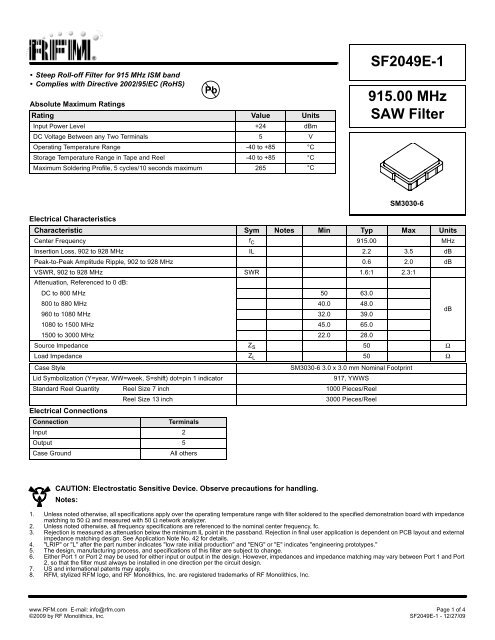
915.00 MHz SAW Filter SF2049E-1 - RF Monolithics, Inc.
915.00 MHz SAW Filter SF2049E-1 - RF Monolithics, Inc.
915.00 MHz SAW Filter SF2049E-1 - RF Monolithics, Inc.

Create successful ePaper yourself
Turn your PDF publications into a flip-book with our unique Google optimized e-Paper software.
• Steep Roll-off <strong>Filter</strong> for 915 <strong>MHz</strong> ISM band<br />
• Complies with Directive 2002/95/EC (RoHS)<br />
Absolute Maximum Ratings<br />
Rating Value Units<br />
Input Power Level +24 dBm<br />
DC Voltage Between any Two Terminals 5 V<br />
Operating Temperature Range -40 to +85 °C<br />
Storage Temperature Range in Tape and Reel -40 to +85 °C<br />
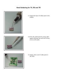
Maximum Soldering Profile, 5 cycles/10 seconds maximum 265 °C<br />
Pb<br />
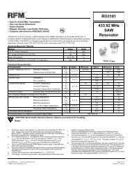
<strong>SF2049E</strong>-1<br />
<strong>915.00</strong> <strong>MHz</strong><br />
<strong>SAW</strong> <strong>Filter</strong><br />
SM3030-6<br />
Electrical Characteristics<br />
Characteristic Sym Notes Min Typ Max Units<br />
Center Frequency f C <strong>915.00</strong> <strong>MHz</strong><br />
Insertion Loss, 902 to 928 <strong>MHz</strong> IL 2.2 3.5 dB<br />
Peak-to-Peak Amplitude Ripple, 902 to 928 <strong>MHz</strong> 0.6 2.0 dB<br />
VSWR, 902 to 928 <strong>MHz</strong> SWR 1.6:1 2.3:1<br />
Attenuation, Referenced to 0 dB:<br />
DC to 800 <strong>MHz</strong> 50 63.0<br />
800 to 880 <strong>MHz</strong> 40.0 48.0<br />
960 to 1080 <strong>MHz</strong> 32.0 39.0<br />
dB<br />
1080 to 1500 <strong>MHz</strong> 45.0 65.0<br />
1500 to 3000 <strong>MHz</strong> 22.0 28.0<br />
Source Impedance Z S 50 Ω<br />
Load Impedance Z L 50 Ω<br />
Case Style<br />
SM3030-6 3.0 x 3.0 mm Nominal Footprint<br />
Lid Symbolization (Y=year, WW=week, S=shift) dot=pin 1 indicator<br />
917, YWWS<br />
Standard Reel Quantity Reel Size 7 inch 1000 Pieces/Reel<br />
Reel Size 13 inch<br />
3000 Pieces/Reel<br />
Electrical Connections<br />
Connection<br />
Terminals<br />
Input 2<br />
Output 5<br />
Case Ground<br />
All others<br />
CAUTION: Electrostatic Sensitive Device. Observe precautions for handling.<br />
Notes:<br />
1. Unless noted otherwise, all specifications apply over the operating temperature range with filter soldered to the specified demonstration board with impedance<br />
matching to 50 Ω and measured with 50 Ω network analyzer.<br />
2. Unless noted otherwise, all frequency specifications are referenced to the nominal center frequency, fc.<br />
3. Rejection is measured as attenuation below the minimum IL point in the passband. Rejection in final user application is dependent on PCB layout and external<br />
impedance matching design. See Application Note No. 42 for details.<br />
4. "LRIP" or "L" after the part number indicates "low rate initial production" and "ENG" or "E" indicates "engineering prototypes."<br />
5. The design, manufacturing process, and specifications of this filter are subject to change.<br />
6. Either Port 1 or Port 2 may be used for either input or output in the design. However, impedances and impedance matching may vary between Port 1 and Port<br />
2, so that the filter must always be installed in one direction per the circuit design.<br />
7. US and international patents may apply.<br />
8. <strong>RF</strong>M, stylized <strong>RF</strong>M logo, and <strong>RF</strong> <strong>Monolithics</strong>, <strong>Inc</strong>. are registered trademarks of <strong>RF</strong> <strong>Monolithics</strong>, <strong>Inc</strong>.<br />
www.<strong>RF</strong>M.com E-mail: info@rfm.com Page 1 of 4<br />
©2009 by <strong>RF</strong> <strong>Monolithics</strong>, <strong>Inc</strong>. <strong>SF2049E</strong>-1 - 12/27/09
CH1 S21 LOG 10 dB/ REF -3.5 dB<br />
<strong>SF2049E</strong><br />
Demo board<br />
CH1 PASS<br />
8 Feb 2005 13:25:41<br />
3 : -38 . 598 dB 960 . 000 000 <strong>MHz</strong><br />
PRm<br />
CH1<br />
Markers<br />
Cor<br />
1 : -2 . 1106 dB<br />
902 . 000 <strong>MHz</strong><br />
2 : -1 . 9379 dB<br />
928 . 000 <strong>MHz</strong><br />
1 2<br />
3<br />
CENTER 915 . 000 000 <strong>MHz</strong> SPAN 300 . 000 000 <strong>MHz</strong><br />
CH1 S21 LOG 10 dB/ REF -3.5 dB<br />
<strong>SF2049E</strong><br />
Demo board<br />
CH1 PASS<br />
8 Feb 2005 13:29:01<br />
PRm<br />
Cor<br />
Hld<br />
START . 010 000 <strong>MHz</strong> STOP 3 000 . 000 000 <strong>MHz</strong><br />
www.<strong>RF</strong>M.com E-mail: info@rfm.com Page 2 of 4<br />
©2009 by <strong>RF</strong> <strong>Monolithics</strong>, <strong>Inc</strong>. <strong>SF2049E</strong>-1 - 12/27/09
SM3030-6 Case<br />
6-Terminal Ceramic Surface-Mount Case<br />
3.0 X 3.0 mm Nominal Footprint<br />
<br />
<br />
<br />
<br />
<br />
<br />
<br />
<br />
<br />
PCB Footprint Top View<br />
Case and PCB Footprint Dimensions<br />
Dimension<br />
mm<br />
<strong>Inc</strong>hes<br />
Min Nom Max Min Nom Max<br />
A 2.87 3.00 3.13 0.113 0.118 0.123<br />
B 2.87 3.00 3.13 0.113 0.118 0.123<br />
C 1.12 1.25 1.38 0.044 0.049 0.054<br />
D 0.77 0.90 1.03 0.030 0.035 0.040<br />
E 2.67 2.80 2.93 0.105 0.110 0.115<br />
F 1.47 1.60 1.73 0.058 0.063 0.068<br />
G 0.72 0.85 0.98 0.028 0.033 0.038<br />
H 1.37 1.50 1.63 0.054 0.059 0.064<br />
I 0.47 0.60 0.73 0.019 0.024 0.029<br />
J 1.17 1.30 1.43 0.046 0.051 0.056<br />
K 3.20 0.126<br />
L 1.70 0.067<br />
M 1.05 0.041<br />
N 0.81 0.032<br />
O 0.38 0.015<br />
Case Materials<br />
Solder Pad<br />
Plating<br />
Lid Plating<br />
Body<br />
Materials<br />
0.3 to 1.0 µm Gold over 1.27 to 8.89 µm Nickel<br />
2.0 to 3.0 µm Nickel<br />
Al 2 O 3 Ceramic<br />
Pb Free<br />
TOP VIEW<br />
BOTTOM VIEW<br />
B<br />
C<br />
G<br />
H<br />
1<br />
6<br />
6<br />
1<br />
A<br />
2<br />
5<br />
E<br />
F<br />
5<br />
2<br />
I<br />
3<br />
4<br />
4<br />
3<br />
D<br />
J<br />
www.<strong>RF</strong>M.com E-mail: info@rfm.com Page 3 of 4<br />
©2009 by <strong>RF</strong> <strong>Monolithics</strong>, <strong>Inc</strong>. <strong>SF2049E</strong>-1 - 12/27/09
12.0<br />
5.5<br />
1.75<br />
100 REF.<br />
"B" REF.<br />
Tape and Reel Specifications<br />
“B “<br />
Quantity Per Reel<br />
<strong>Inc</strong>hes millimeters<br />
7 178 1000<br />
13 330 3000<br />
See Detail "A"<br />
12.0<br />
13.0<br />
2.0<br />
20.2<br />
COMPONENT ORIENTATION and DIMENSIONS<br />
Carrier Tape Dimensions<br />
Ao<br />
Bo<br />
Ko<br />
Pitch<br />
W<br />
3.35 mm<br />
3.35 mm<br />
1.40 mm<br />
8.0 mm<br />
12.0 mm<br />
0.3 ± 0.05<br />
PIN #1<br />
2.0 4.0<br />
1.50<br />
A<br />
RO.3<br />
(MAX.)<br />
Bo<br />
B<br />
B<br />
Ko<br />
Ao<br />
Pitch<br />
A<br />
R0.5<br />
(MAX.)<br />
1.5<br />
SECTION A-A<br />
SECTION B-B<br />
USER DIRECTION OF FEED<br />
www.<strong>RF</strong>M.com E-mail: info@rfm.com Page 4 of 4<br />
©2009 by <strong>RF</strong> <strong>Monolithics</strong>, <strong>Inc</strong>. <strong>SF2049E</strong>-1 - 12/27/09