TRC101 300-1000 MHz Transceiver - RF Monolithics, Inc.
TRC101 300-1000 MHz Transceiver - RF Monolithics, Inc.
TRC101 300-1000 MHz Transceiver - RF Monolithics, Inc.

Create successful ePaper yourself
Turn your PDF publications into a flip-book with our unique Google optimized e-Paper software.
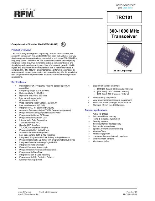
<strong>TRC101</strong><strong>300</strong>-<strong>1000</strong> <strong>MHz</strong><strong>Transceiver</strong>Complies with Directive 2002/95/EC (RoHS)Product Overview<strong>TRC101</strong> is a highly integrated single chip, zero-IF, multi-channel, lowpower <strong>RF</strong> transceiver. It is an ideal fit for low cost, high volume, two wayshort-range wireless applications for use in the unlicensed <strong>300</strong>-<strong>1000</strong> <strong>MHz</strong>frequency bands. All critical <strong>RF</strong> and baseband functions are completelyintegrated in the chip, thus minimizing external component count andsimplifying and speeding design-ins. Use of a low cost, generic 10<strong>MHz</strong>crystal and a low-cost microcontroller is all that is needed to create acomplete link. The <strong>TRC101</strong> also incorporates different sleep modes toreduce overall current consumption and extend battery life. Its small sizewith low power consumption makes it ideal for various short range radioapplications.Key Features• Modulation: FSK (Frequency Hopping Spread Spectrumcapability)• Frequency range: <strong>300</strong>-<strong>1000</strong> <strong>MHz</strong>• High sensitivity: (-105 dBm)• High data rate: Up to 256 kbps• Low current consumption(RX current ~8.5mA)• Wide operating supply voltage: 2.2 to 5.4V• Low standby current (0.2uA)• Integrated PLL, IF, Baseband Circuitry• Automatic Frequency Adjust(TX/RX frequency alignment)• Programmable Analog/Digital Baseband Filter• Programmable Output <strong>RF</strong> Power• Programmable Input LNA Gain• Internal Valid Data Recognition• Transmit/Receive FIFO• Standard SPI Interface• TTL/CMOS Compatible I/O pins• Programmable CLK Output Freq• Automatic Antenna tuning circuit• Low cost, generic 10<strong>MHz</strong> Xtal reference• Integrated, Programmable Low Battery Voltage Detector• Programmable Wake-up Timer with programmable Duty Cycle• Integrated Selectable Analog/Digital RSSI• Integrated Crystal Oscillator• External Processor Interrupt pin• Programmable Crystal Load Capacitance• Programmable Data Rate• Integrated Clock & Data Recovery• Programmable FSK Deviation Polarity• External Wake-up Events• Support for Multiple Channels• [315/433 Bands] 95 Channels (100kHz)• [868 Band] 190 Channels (100kHz)• [915 Band] 285 Channels (100kHz)• Power-saving sleep mode• Very few external components requirement• Small size plastic package: 16-pin TSSOP• Standard 13 inch reel, 2000 pieces.Popular applications16-TSSOP package• Active <strong>RF</strong>ID tags• Automated Meter reading• Home & Industrial Automation• Security systems• Two way Remote keyless entry• Automobile Immobilizers• Sports & Performance monitoring• Wireless Toys• Medical equipment• Low power two way telemetry systems• Wireless mesh sensors• Wireless moduleswww.<strong>RF</strong>M.com Email: info@rfm.com Page 1 of 42©by <strong>RF</strong> <strong>Monolithics</strong>, <strong>Inc</strong>. <strong>TRC101</strong> - 4/8/08
Table of ContentsTable of Contents.......................................................................................................... 11.0 <strong>TRC101</strong> Pin Configuration...................................................................................... 21.1 Pin Description..................................................................................................... 32.0 Functional Description ........................................................................................... 42.1 <strong>TRC101</strong> Applications ........................................................................................... 4<strong>RF</strong> Transmitter Matching ..................................................................................... 4Antenna Design Considerations........................................................................... 5PCB Layout Considerations................................................................................. 53.0 <strong>TRC101</strong> Functional Characteristics ....................................................................... 7Input/Output Amplifier ................................................................................................ 7Baseband Data and Filtering ..................................................................................... 7Transmit Register....................................................................................................... 8Receive FIFO............................................................................................................. 8Automatic Frequency Adjustment (AFA).................................................................... 9Crystal Oscillator........................................................................................................ 9Frequency Control (PLL) and Frequency Synthesizer ............................................... 9Data Quality Detector (DQD) ..................................................................................... 9Valid Data Detector ................................................................................................. 10Receive Signal Strength Indicator (RSSI) ................................................................ 10OOK/ASK Signaling ................................................................................................. 10Wake-Up Mode........................................................................................................ 10Low Battery Detector ............................................................................................... 10SPI Interface ............................................................................................................ 114.0 Control and Configuration Registers .................................................................. 13Status Register ....................................................................................................... 14Configuration Register [POR=8008h] .......................................................................... 15Automatic Frequency Adjust Register [POR=C4F7h] .................................................. 16Transmit Configuration Register [POR=9800h] ........................................................... 18Transmit Register [POR=B8AAh] ................................................................................ 19Frequency Setting Register [POR=A680h] .................................................................. 20Receiver Control Register [POR=9080h]..................................................................... 21Baseband Filter Register [POR=C22Ch] ..................................................................... 23FIFO Read Register [POR=B000h] ............................................................................. 24FIFO and RESET Mode Configuration Register [POR=CA80h]................................... 25Data Rate Setup Register [POR=C623h]..................................................................... 26Power Management Register [POR=8208h]................................................................ 27Wake-up Timer Period Register [POR=E196h] ........................................................... 28Duty Cycle Set Register [POR=C80Eh]....................................................................... 29Battery Detect Threshold and Clock Output Register [POR=C000h]........................... 305.0 Maximum Ratings.................................................................................................. 316.0 DC Electrical Characteristics ............................................................................... 317.0 AC Electrical Characteristics ............................................................................... 328.0 Receiver Measurement Results ........................................................................... 359.0 Transmitter Measurement Results....................................................................... 36Reflow Profile .............................................................................................................. 3710.0 Package Information ........................................................................................... 38www.<strong>RF</strong>M.com Email: info@rfm.com Page 2 of 42©by <strong>RF</strong> <strong>Monolithics</strong>, <strong>Inc</strong>. <strong>TRC101</strong> - 4/8/08
1. Pin Configuration1.1 Pin DescriptionsSDISCKnCSSDOIRQDATA/nFSELCR/FINT/FCAPCLKOUT12345678TOP VIEW<strong>TRC101</strong>161514131211109nINT/DDETRSSIAVDD<strong>RF</strong>_N<strong>RF</strong>_PGNDRESETXtal/RefPin Name Description1 SDI SPI Data In2 SCK SPI Data Clock3 nCS Chip Select Input – Selects the chip for an SPI data transaction. The pin must be pulled ‘low’ for a 16-bit read or write function. See Figure 6 for timing specifications.4 SDO SPI Data Out5 nIRQ Interrupt Request Output - The receiver will generate an active low interrupt request for themicrocontroller on the following events:· The TX register is ready to receive the next byte· The FIFO has received the preprogrammed amount of bits· Power-on reset· FIFO overflow/TX register underrun· Wake-up timer timeout· Negative pulse on the interrupt input pin nINT· Supply voltage below the preprogrammed value is detected6 Data/nFSel Data In – When the internal TX register is not used, this pin may be used to manually modulate datafrom an external host processor. If the internal TX register is enabled, this pin must be pulled “High”.When using the internal Rx FIFO, this pin must be pulled “Low” to select the FIFO. This pin is used toselect the internal registers when reading and writing.Data Out – When the internal FIFO is not used this pin is used in conjunction with pin 7 (RecoveredClock) to receive data.FIFO Select – When reading the FIFO, this pin selects the FIFO and the first bit appears on the nextclock. Use this pin in conjunction with Pin 7.7 CR/FINT/FCAP Recovered Clock Output – When the digital filter is used (Baseband Filter Register, Bit [4]) and FIFOdisabled (Configuration Register, Bit [6]), this pin provides the recovered clock from the incoming data.FIFO INT – When the internal FIFO is enabled (Configuration Register, Bit [6]), this pin acts as a FIFOFull interrupt indicating that the FIFO has filled to its pre-programmed limit (FIFO Configuration Register,Bit [7..4]).External Data Filter Capacitor – When the Analog filter is used (Baseband Filter Register, Bit [4]), thispin is the raw baseband data that may be used by a host processor for data recovery. The externalcapacitor forms a simple lowpass filter with an internal 10KOhm series resistor. The capacitor valuemay be chosen for a Max data rate up to 256kbps.8 ClkOut Optional host processor Clock Output9 Xtal/Ref Xtal - Connects to a 10<strong>MHz</strong> series crystal or an external oscillator reference. The circuit contains anintegrated load capacitor (See Configuration Register) in order to minimize the external componentcount. The crystal is used as the reference for the PLL, which generates the local oscillator frequency.The accuracy requirements for production tolerance, temperature drift and aging can be determinedfrom the maximum allowable local oscillator frequency error. Whenever a low frequency error isessential for the application, it is possible to “pull” the crystal to the accurate frequency by changing theload capacitor value.Ext Ref – An external reference, such as an oscillator, may be connected as a reference source.Connect through a .01uF capacitor.10 nRESET Reset Output with internal pull-up11 GND System Ground12 <strong>RF</strong>_P <strong>RF</strong> Diff I/O13 <strong>RF</strong>_N <strong>RF</strong> Diff I/O14 VDD Supply Voltage15 RSSIA Analog RSSI Output – The Analog RSSI can be used to determine the actual signal strength. Theresponse and settling time depends on an external filter capacitor. Typically, a <strong>1000</strong>pF capacitor willprovide optimum response time for most applications.16 nINT/DDet nINT – This pin may be configured as an active low external interrupt to the chip. When a logic ‘0’ isapplied to this pin, it causes the nIRQ pin (5) to toggle, signaling an interrupt to an external processor.Reading the first four (4) bits of the status register tells the source of the interrupt. This pin may be usedas a wake-up event from sleep.Valid Data Detector Output– This pin may be configured to indicate Valid Data when the synchronouswww.<strong>RF</strong>M.com Email: info@rfm.com Page 3 of 42©by <strong>RF</strong> <strong>Monolithics</strong>, <strong>Inc</strong>. <strong>TRC101</strong> - 4/8/08
pattern recognition circuit indicates potentially real incoming data.2. Functional DescriptionThe <strong>TRC101</strong> is a low power, frequency agile, zero-IF, multi-channel FSK transceiver for use in the 315,433, 868, and 916 <strong>MHz</strong> bands. All <strong>RF</strong> and baseband functions are completely integrated requiring only asingle 10<strong>MHz</strong> crystal as a reference source and an external low-cost processor. Functions include:• PLL synthesizer• Power Amp• LNA• I/Q Mixers• I/Q Demodulators• Baseband Filters• Baseband Amplifiers• RSSI• Low Battery Detector• Wake-up Timer/Duty Cycle Mode• Valid Data Detection/Data QualityThe <strong>TRC101</strong> is ideal for Frequency Hopping Spread Spectrum (FHSS) applications requiring frequencyagility to meet FCC requirements. Use of a low-cost microcontroller is all that is needed to create acomplete data link. The <strong>TRC101</strong> incorporates different sleep modes to reduce overall currentconsumption and extend battery life. It is ideal for applications operating from typical lithium coin cells.2.1 <strong>TRC101</strong> Typical Application Circuit<strong>RF</strong> Transmitter MatchingFigure 1. Typical Application CircuitThe <strong>RF</strong> pins are high impedance and differential. The optimum differential load for the <strong>RF</strong> port at a givenfrequency band is shown in Table 1.TABLE 1.<strong>TRC101</strong> Admittance Impedance (Ohm) L315 <strong>MHz</strong> 1.5e-3 – j5.14e-3 52 + j179 98nH433 <strong>MHz</strong> 1.4e-3 – j7.1e-3 27 + j136 52nH868 <strong>MHz</strong> 2e-3 – j1.5e-2 8.7 + j66 12.5nHwww.<strong>RF</strong>M.com Email: info@rfm.com Page 4 of 42©by <strong>RF</strong> <strong>Monolithics</strong>, <strong>Inc</strong>. <strong>TRC101</strong> - 4/8/08
916 <strong>MHz</strong> 2.2e-3 – j1.55e-2 9 + j63 11.2nHThese values are what the <strong>RF</strong> port pins want to “see” as an antenna load for maximum power transfer.Antennas ideally suited for this would be a Dipole, Folded Dipole, and Loop. For all transmit antennaapplications a bias or “choke” inductor must be included since the <strong>RF</strong> outputs are open-collector type.The <strong>TRC101</strong> may also drive a single ended 50 Ohm load, such as a monopole antenna, using thematching circuit as shown in Figure 1. Use of a balun would provide an optimum power transfer, but thematching circuit of Figure 1 has been optimized for use with discrete components, reducing the costassociated with use of a balun. The matching component values for a 50 Ohm load for each band aregiven in Table 2.Table 2.Ref Des 315 433 868 916C1 6.8pF 5.1pF 2.7pF 2.7pFC2 3.9pF 2.7pF 1.2pF 1.2pFC4 .1uF .1uF .1uF .1uFC7 100pF 100pF 100pF 100pFL1 56nH 33nH 8.2nH 8.2nHL2 390nH 390nH 100nH 100nHL3 68nH 47nH 22nH 22nHAntenna Design ConsiderationsThe <strong>TRC101</strong> is designed to drive a differential output such as a Dipole antenna or a Loop. The loopantenna is ideally suited for applications where compact size is required. The dipole is typically not anattractive option for compact designs due to its inherent size at resonance and distance needed awayfrom a ground plane to be an efficient antenna. A monopole antenna can be used with the addition of abalun or by using the matching circuit in Figure 1.PCB Layout ConsiderationsOptimal PCB layout is very critical. For optimal transmit and receive performance, the trace lengths at the<strong>RF</strong> pins must be kept as short as possible. Using small, surface mount components, like 0402 or 0603,will yield the best performance as well as keep the <strong>RF</strong> port compact. Make all <strong>RF</strong> connections short anddirect. A good rule of thumb to adhere to is add 1nH of series inductance for every 0.1” of trace length.The crystal oscillator is also affected by additional trace length as it adds parasitic capacitance to theoverall load of the crystal. To minimize this effect place the crystal as close as possible to the chip andmake all connections short and direct. This will minimize the effects of “frequency pulling” that straycapacitance may introduce and allows the internal load capacitance of the chip to be more effective inproperly loading the crystal oscillator circuit.If using an external processor, the <strong>TRC101</strong> provides an on-chip clock for that purpose. Even though thisis an integrated function, long runs of the clock signal may radiate and cause interference. This candegrade receiver performance as well as add harmonics or unwanted modulation to the transmitter.Keep clock connections as short as possible and surround the clock trace with an adjacent ground planepour where needed. This will help in reducing any radiation or crosstalk due to long runs of the clocksignal.Good power supply bypassing is also essential. Large decoupling capacitors should be placed at thepoint where power is applied to the PCB. Smaller value decoupling capacitors should then be placed ateach power point of the chip as well as bias nodes for the <strong>RF</strong> port. Poor bypassing lends itself toconducted interference which can cause noise and spurious signals to couple into the <strong>RF</strong> sections,significantly reducing performance.www.<strong>RF</strong>M.com Email: info@rfm.com Page 5 of 42©by <strong>RF</strong> <strong>Monolithics</strong>, <strong>Inc</strong>. <strong>TRC101</strong> - 4/8/08
Assembly ViewTop SideBottom Sidewww.<strong>RF</strong>M.com Email: info@rfm.com Page 6 of 42©by <strong>RF</strong> <strong>Monolithics</strong>, <strong>Inc</strong>. <strong>TRC101</strong> - 4/8/08
3. <strong>TRC101</strong> Functional CharacteristicsLN A0/ 90I/QDEMODFSKASK+-SDISDOSCKnC S<strong>RF</strong> _P<strong>RF</strong> _NTX/RXRSSICONTROLLO G I CnI R QDATA / nF SELCR/F INT/F CAPPAVCOPLLOSCCLKOUTnINT/DDET/NBATT DETRXTAL/REF RSSIAVDD GNDnRESETFigure 2. Functional Block DiagramInput/Output AmplifierThe output power amplifier is an open-collector, differential output with programmable output power whichcan directly drive a loop or dipole antenna, and with proper matching may also drive a monopole antenna.<strong>Inc</strong>orporated in the power amplifier is an automatic antenna tuning circuit to avoid manual tuning duringproduction and to offset “hand effects”. Registers common to the Power Amplifier are:• Power Management Register• Transmit Configuration RegisterThe input LNA has selectable gain (0dB, -6dB, -14dB, -20dB) which may be useful in an environment withstrong interferers. The LNA has a 250ΩOhm differential input impedance which requires a matchingcircuit when connected to 50 Ohm devices. Registers common to the LNA are:• Power Management Register• Receiver Control RegisterBaseband Data and FilteringThe baseband receiver has several programmable options that optimize the data link for a wide range ofapplications. The programmable functions include:• Receive bandwidth• Receive data rate• Baseband Analog Filter• Baseband Digital Filter• Clock Recovery (CR)• Receive FIFO• Data Quality Detector• Valid Data DetectorThe receive bandwidth is programmable from 67kHz to 400kHz to accommodate various FSK modulationdeviations. If the deviation is known for a given transmitter, the best results are obtained with abandwidth at least twice the transmitter FSK deviation.www.<strong>RF</strong>M.com Email: info@rfm.com Page 7 of 42©by <strong>RF</strong> <strong>Monolithics</strong>, <strong>Inc</strong>. <strong>TRC101</strong> - 4/8/08
The receive data rate is programmable from 337bps to 256kbps. An internal prescaler is used to givebetter resolution when setting up the receive data rate. The prescaler is optional and may be disabledthrough the Data Rate Setup Register.The type of baseband filtering is selectable between an Analog filter and a Digital filter. The analog filteris a simple RC lowpass filter. An external capacitor may be chosen depending on the actual data rate.The chip has an integrated 10K Ohm resistor in series that makes the RC lowpass network. With theanalog filter selected, a maximum data rate of 256kbps can be achieved. The digital filter is used with aclock frequency of 29X data rate. In this mode a clock recovery (CR) circuit is used to provide for asynchronized clock source to recover the data using an external processor. The CR has three modes ofoperation: fast, slow, and automatic, all configurable through the Baseband Filter Register. The CRcircuit works by sampling the preamble on the incoming data. The preamble must contain a series of 1’sand 0’s in order for the CR circuit to properly extract the data timing. In slow mode the CR circuit requiresmore sampling (12 to 16 bits) and thus has a longer settling time before locking. In fast mode the CRcircuit takes fewer samples (6 to 8 bits) before locking so settling time is not as long and timing accuracyis not critical. In automatic mode the CR circuit begins in fast mode to coarsely acquire the timing periodwith fewer samples and then changes to slow mode after locking. Further details of the CR and data rateclock are provided in the Baseband Filter Register. CR is only used with the digital filter and data rateclock. These are not used when configured for the analog filter.Transmit RegisterThe transmit register is configured as two 8-bit shift registers connected in series to form a single 16-bitshift register. On POR the registers are filled with the value AAh. This can be used to generate apreamble before sending actual data, however, the value is not reloaded when the transmit register is reenabled.When the transmitter is enabled through the Power Management Register, transmission beginsimmediately and the value in the transmit register begins to be sent out. If there is nothing written to theregister then it will send out the default value AAh. The next data byte can be loaded via the SPI bus tothe transmit register by monitoring the SDO pin for a logic ‘1’ or waiting for an interrupt from the nIRQ pin.After data has been loaded to the transmit register the processor must wait for the next interrupt beforedisabling the transmitter or the rest of the data left in the register will be lost. Inserting a dummy byte ofall 0’s is recommended for the last byte of data loaded.Receive FIFOThe receive FIFO is configured as one 16-bit register. The FIFO can be configured to generate aninterrupt after a predefined number of bits have been received. This threshold is programmable from 1 to16 bits (0..15). It is recommended to set the threshold to at least half the length of the register (8 bits) toinsure the external host processor has time to set up before performing a FIFO read. The FIFO readclock (SCK) must be < fXTAL/4 or
The FIFO can be read out through the SDO pin only by pulling the nFSEL pin (6) ‘Low” which selects theFIFO for read and reading out data on the next SPI clock. The FINT pin (7) will stay active (logic ‘1’) untilthe last bit has been read out, and it will then go ‘low’. This pin may also be polled to watch for valid data.When the number of bits received in the FIFO match the pre-programmed limit, this pin will go active(logic ‘1’) and stay active until the last bit is read out as above. An alternative method of reading the FIFOis through an SPI bus Status Register read. The drawback to this is that all interrupt and status bits mustbe read first before the FIFO bits appear on the bus. This could pose a problem for receiving largeamounts of data. The best method is using the SDO pin and the associated FIFO function pins.Automatic Frequency Adjustment (AFA)The PLL has the capability to do fine adjustment of the carrier frequency automatically. In this way, thereceiver can minimize the offset between transmit and receive frequency. This function may be enabledor disabled through the Automatic Frequency Adjustment Register. The range of offset can beprogrammed as well as the offset value calculated and added to the frequency control word within thePLL to incrementally change the carrier frequency. The chip can be programmed to automaticallyperform an adjustment or may be manually activated by a strobe signal. This function has the advantageof allowing:• Low cost lower accuracy crystals to be used• <strong>Inc</strong>reased receiver sensitivity by narrowing the receive bandwidth• Achieving higher data ratesCrystal OscillatorThe <strong>TRC101</strong> incorporates an internal crystal oscillator circuit that provides a 10<strong>MHz</strong> reference, as well asinternal load capacitors. This significantly reduces the component count required. The internal loadcapacitance is programmable from 8.5pF to 16pF in 0.5pF steps. This has the advantage of accepting awide range of crystals from many different manufacturers having different load capacitance requirements.Being able to vary the load capacitance also helps with fine tuning the final carrier frequency since thecrystal is the PLL reference for the carrier.An external clock signal is also provided that may be used to run an external processor. This also hasthe advantage of reducing component count by eliminating an additional crystal for the host processor.The clock frequency is also programmable from eight pre-defined frequencies, each a pre-scaled value ofthe 10<strong>MHz</strong> crystal reference. These values are programmable through the Battery Detect Threshold andClock Output Register. The internal clock oscillator may be disabled which also disables the output clocksignal to the host processor. When the oscillator is disabled, the chip provides an additional 196 clockcycles before releasing the output, which may be used by the host processor to setup any functionsbefore going to sleep.Frequency Control (PLL) and Frequency SynthesizerThe PLL synthesizer is the heart of the operating frequency. It is programmable and completelyintegrated, providing all functions required to generate the carriers and tunability for each band. The PLLrequires only a single 10<strong>MHz</strong> crystal reference source. <strong>RF</strong> stability is controlled by choosing a crystalwith the particular specifications to satisfy the application. This gives the designer the maximum flexibilityin performance.The PLL is able to perform manual and automatic calibration to compensate for changes in temperatureor operating voltage. When changing band frequencies, re-calibration must be performed. This can bedone by disabling the synthesizer and re-enabling again through the Power Management Register.Registers common to the PLL are:• Power Management Register• Configuration Register• Frequency Setting Register• Automatic Frequency Adjust Register• Transmit Configuration RegisterData Quality Detector (DQD)www.<strong>RF</strong>M.com Email: info@rfm.com Page 9 of 42©by <strong>RF</strong> <strong>Monolithics</strong>, <strong>Inc</strong>. <strong>TRC101</strong> - 4/8/08
The DQD is a unique function of the <strong>TRC101</strong>. The DQD circuit looks at the prefiltered incoming data andcounts the “spikes” of noise for a predetermined period of time to get an idea of the quality of the link.This parameter is programmable through the Data Filter Command Register. The DQD count threshold isprogrammable from 0 to 7 counts. The higher the count the lower the quality of the data link. This meansthe higher the content of noise spikes in the data stream the more difficult it will be to recover clockinformation as well as data.Valid Data DetectorThe DDET is an extension of the DQD. When incoming data is detected, it uses the DQD signal, theClock Recovery Lock signal, and the Digital RSSI signal to determine if the incoming data is valid. TheDDET looks for valid data transitions at an expected data rate. The desired data rate and the acceptancecriteria for valid data are user programmable through the SPI port. The DDET signal is valid when usingeither the internal receive FIFO or an external pin to capture baseband data. The DDET has three modesof operation: slow, medium, fast. Each mode is dependent on what signals it uses to determine valid dataas well as the number of incoming preamble bits present at the beginning of the packet. The DDET canbe disabled by the user so that only raw data from the comparator comes out, or it can be set to acceptonly a preset range of data rates and data quality. The DDET saves battery power and time for a hostmicroprocessor because it will not wake up the microprocessor unless there is valid data present. Seethe Receiver Control Register for a detailed description of the setup for valid data.Receive Signal Strength Indicator (RSSI)The <strong>TRC101</strong> provides an analog RSSI and a digital RSSI. The digital RSSI threshold is programmablethrough the Receiver Control Register and is readable through the Status Register only. When anincoming signal is stronger than the preprogrammed threshold, the digital RSSI bit in the Status Registeris set.1.2Input Power vs RSSI Voltage10.8RSSI (V)0.60.40.20-112 -102 -92 -82 -72 -62 -52 -42Input Power (dBm)The analog RSSI is available through the RSSIA external pin (15). This pin requires an external capacitorwhich sets the settling time. The analog RSSI may be used to recover OOK/ASK modulated data. TheRSSI level is linear with input signal levels between -100 dBm and -55 dBm. The external capacitor valuewill control the received ASK data rate allowed so choosing a lower value capacitor enables recovery offaster data at the expense of amplitude. Using pin (15) with a sensitive comparator will yield good results.The analog RSSI is available through and external pin (15). This pin requires an external capacitor whichsets the settling time. The analog RSSI may be used to recover ASK modulated data at a low rate on theorder of a few thousand bits per sec. The external capacitor value will control the received ASK data rateallowed so choosing a lower value capacitor enables recovery of faster data at the expense of amplitude.Using pin (15) with a sensitive comparator will yield good results.www.<strong>RF</strong>M.com Email: info@rfm.com Page 10 of 42©by <strong>RF</strong> <strong>Monolithics</strong>, <strong>Inc</strong>. <strong>TRC101</strong> - 4/8/08
OOK/ASK SignalingThe RSSI may be used to recover an OOK/ASK signal using an external comparator, capacitivelycoupled to the RSSI output. Typically, Automatic Gain Control (AGC) is used to reduce the input signallevel upon saturation of the RSSI in the presence of strong or near-field ASK signals. The <strong>TRC101</strong> doesnot have an AGC option, however, the input LNA gain is programmable. The output RSSI signal levelmay be sampled upon enabling of the receiver to test if the signal level is in saturation. If saturation isconfirmed, the input LNA gain may be reduced until the RSSI output signal level falls within the RSSIdeviation range.Wake-Up ModeThe <strong>TRC101</strong> has an internal wake-up timer that has very low current consumption (1.5uA typical) andmay be programmed from 1ms to several days. A calibration is performed to the crystal at startup andevery 30 sec thereafter, even if in sleep mode. If the oscillator circuit is disabled the calibration circuit willturn it on briefly to perform a calibration to maintain accurate timing and return to sleep.The <strong>TRC101</strong> also incorporates other power saving modes aside from the wake-up timer. Return to activemode may be initiated from several external events:• Logic ‘0’ applied to nINT pin (16)• Low Supply Voltage Detect• FIFO Fill• SPI requestIf any of these wake-up events occur, including the wake-up timer, the <strong>TRC101</strong> generates an externalinterrupt on the nIRQ pin (5) which may be used as a wake-up signal to a host processor. The source ofthe interrupt may be read out from the Status Register over the SPI bus.Duty Cycle ModeThe duty cycle register may be used in conjunction with the wake-up timer to reduce the average currentconsumption of the receiver. The duty cycle register may be set up so that when the wake-up timerbrings the chip out of sleep mode the receiver is turned on for a short time to sample if a signal is presentand then goes back into sleep and the process starts over. See the Duty Cycle Set Register. Thereceiver must be disabled (RXEN bit 7 cleared in Power Management Register) and the wake-up timermust be enabled (WKUPEN bit 1 set in Power Management Register) for operation in this mode. Figure6 shows the timing for Duty Cycle Mode.Figure 6. Duty Cycle Mode TimingLow Battery DetectorThe integrated low battery detector monitors the voltage supply against a preprogrammed value andgenerates an interrupt when the supply voltage falls below the programmed value. The detector circuithas 50mV of hysteresis built in.SPI Interfacewww.<strong>RF</strong>M.com Email: info@rfm.com Page 11 of 42©by <strong>RF</strong> <strong>Monolithics</strong>, <strong>Inc</strong>. <strong>TRC101</strong> - 4/8/08
The <strong>TRC101</strong> is equipped with a standard SPI bus that is compatible to almost all SPI devices. Allfunctions and status of the chip are accessible through the SPI bus. Typical SPI devices are configuredfor byte write operations. The <strong>TRC101</strong> uses word writes so the nCS pin(3) should be pulled low for 16bits.Figure 3. SPI Interface Timingwww.<strong>RF</strong>M.com Email: info@rfm.com Page 12 of 42©by <strong>RF</strong> <strong>Monolithics</strong>, <strong>Inc</strong>. <strong>TRC101</strong> - 4/8/08
4. Control and Configuration RegistersBit Bit Bit Bit Bit Bit Bit Bit Bit Bit Bit Bit Bit Bit Bit Bit15 14 13 12 11 10 9 8 7 6 5 4 3 2 1 0STATUS FIFTXRX POR FIFOV/UR WKINT INTRST LB FIFEMP RSSI/AT GDQD CRLK AFATGL OFFSGN OFF3 OFF2 OFF1 OFF0 - -CONFIG 1 0 0 0 0 0 0 0 DATEN FIFEN BAND1 BAND0 CAP3 CAP2 CAP1 CAP0 8008hAFA 1 1 0 0 0 1 0 0 AUTO1 AUTO0 RNG1 RNG0 STRB ACCF OFFEN AFEN C4F7hTX CONFIG 1 0 0 1 1 0 0 MODP DEV3 DEV2 DEV1 DEV0 0 PWR2 PWR1 PWR0 9800hTX REG 1 0 1 1 1 0 0 0 TX7 TX6 TX5 TX4 TX3 TX2 TX1 TX0 B8AAhFREQ SET 1 0 1 0 Freq11 Freq10 Freq9 Freq8 Freq7 Freq6 Freq5 Freq4 Freq3 Freq2 Freq1 Freq0 A680hRECV CTRL 1 0 0 1 0 INT/VDI VDIR1 VDIR0 BB2 BB1 BB0 GAIN1 GAIN0 RSSI2 RSSI1 RSSI0 9080hBASEBAND 1 1 0 0 0 0 1 0 CRLK CRLC 1 FILT 1 DQLVL2 DQLVL1 DQLVL0 C22ChFIFO READ 1 0 1 1 0 0 0 0 RX7 RX6 RX5 RX4 RX3 RX2 RX1 RX0 B000hFIFO/RESETCONFIG1 1 0 0 1 0 1 0 FINT3 FINT2 FINT1 FINT0 0 FIFST FILLEN RSTEN CA80hDATA RATESET1 1 0 0 0 1 1 0 PRE BITR6 BITR5 BITR4 BITR3 BITR2 BITR1 BITR0 C623hPOWERMANAGEMENT1 0 0 0 0 0 1 0 RXEN BBEN TXEN SYNEN OSCEN LBDEN WKUPEN CLKEN 8208hWAKE-UPPERIOD1 1 1 R4 R3 R2 R1 R0 MUL7 MUL6 MUL5 MUL4 MUL3 MUL2 MUL1 MUL0 E196hDUTY CYCLESET1 1 0 0 1 0 0 0 DC6 DC5 DC4 DC3 DC2 DC1 DC0 DCEN C80EhBATT DETECT 1 1 0 0 0 0 0 0 CLK2 CLK1 CLK0 LBD4 LBD3 LBD2 LBD1 LBD0 C000hPORValuewww.<strong>RF</strong>M.com Email: info@rfm.com Page 13 of 42©by <strong>RF</strong> <strong>Monolithics</strong>, <strong>Inc</strong>. <strong>TRC101</strong> - 4/8/08
Status Register (Read Only)Bit Bit Bit Bit Bit Bit Bit Bit Bit Bit Bit Bit Bit Bit Bit Bit15 14 13 12 11 10 9 8 7 6 5 4 3 2 1 0FIFTXRX POR FIFOV/UR WKINT INTRST LB FIFEMP RSSI/AT GDQD CRLCK AFATGL OFFSGN OFF3 OFF2 OFF1 OFF0The Status Register provides feedback for:• FIFO ready/full/empty/under run/overwrite• POR• Interrupt state• Low Battery• Good Data Quality• Digital RSSI signal level• Clock Recovery• Frequency Offset value and sign• AFANote: The Status Register read command begins with a logic ‘0’ where all other register commands begin with a logic ‘1’.Bit [15]:FIFTXRX – When set, indicates the transmit register is ready to receive the next byte for transmission (Transmit Mode) orthat the Rx FIFO has reached the preprogrammed limit (Receive Mode). This bit is multiplexed and dependenton whether you are in the respective Transmit or Receive mode. (Cleared when FIFO read).Bit [14]:POR – When set, Power-on Reset occurred. (Cleared after Status Reg read).Bit [13]:FIFOV/UR – When set, indicates transmit register under run or register overwrite (Transmit Mode) or receive FIFO overflow(Receive Mode). (Cleared after Status Reg read).Bit [12]:WKINT – When set, indicates a Wake-up timer overflow. (Cleared after Status Reg read).Bit [11]:EXINT – When set, indicates a High to Low logic level change on interrupt pin (pin 16). (Cleared after Status Reg read).Bit [10]:LB – When set, indicates the supply voltage is below the preprogrammed limit. See Battery Detect Threshold and ClockOutput Register.Bit [9]:FIFEMP – When set, indicates receive FIFO is empty.Bit [8]:RSSI(Rx) – When set and chip in receive mode, this bit indicates that the incoming <strong>RF</strong> signal is above the preprogrammedDigital RSSI limit.AT(TX) – When in transmit mode this bit indicates that the antenna tuning circuit has detected a strong enough <strong>RF</strong> signal.Bit [7]:GDQD – When set, indicates good data quality.Bit [6]:CRLCK – When set, indicates Clock Recovery is locked.Bit [5]:AFATGL – For each AFC cycle run, this bit will toggle between logic ‘1’ and logic ‘0’.Bit [4]:OFFSGN – Indicates the difference in frequency is higher (logic ‘1’) or lower (logic ‘0’) than the chip frequency.Bit [3..0]:OFF[3..0] – The offset value to be added to the frequency control word (internal PLL). In order to get accurate values theAFA has to be disabled during the read by clearing the "AFEN" bit in the AFA Register (bit 0).To read the status register, initiate a command beginning with a ‘0’ and read the remaining bits on the SDO line. All othercommands begin with a ‘1’ so the <strong>TRC101</strong> recognizes a command vs. status. See figure 4 for timing reference.www.<strong>RF</strong>M.com Email: info@rfm.com Page 14 of 42©by <strong>RF</strong> <strong>Monolithics</strong>, <strong>Inc</strong>. <strong>TRC101</strong> - 4/8/08
Figure 4. Status Read Timingwww.<strong>RF</strong>M.com Email: info@rfm.com Page 15 of 42©by <strong>RF</strong> <strong>Monolithics</strong>, <strong>Inc</strong>. <strong>TRC101</strong> - 4/8/08
Configuration Register [POR=8008h]Bit Bit Bit Bit Bit Bit Bit Bit Bit Bit Bit Bit Bit Bit Bit Bit15 14 13 12 11 10 9 8 7 6 5 4 3 2 1 01 0 0 0 0 0 0 0 DATEN FIFEN BAND1 BAND0 CAP3 CAP2 CAP1 CAP0The configuration register sets up the following:• Internal Data Register• Internal FIFO• Frequency Band in use• Crystal Load capacitanceBit [15..8] – Command Code: These bits are the command code that is sent serially to the processorthat identifies the bits to be written to the configuration register.Bit [7] – TX Data Register Enable: This bit enables the internal TX data register when set. If the internalTX data register is used, the DATA/nFSEL pin (6) must be pulled “High”.Bit [6] – FIFO Enable: This bit enables the internal data FIFO when set. If the data FIFO is enabled, theDATA/nFSEL pin (6) must be pulled “Low”. The FIFO is used to store data during receive. If the FIFO isdisabled by clearing this bit, pin 6 (Data) and pin 7 (Recovered Clock) are used to receive data.Bit [5..4] – Band Select: These bits set the frequency band to be used. There are four (4) bands that aresupported. See Table 3 below for Band configuration.TABLE 3.Frequency Band BAND1 BAND0315 0 0433 0 1868 1 0916 1 1Bit [3..0] – Load Capacitance Select: These bits set the load capacitance for the crystal reference. Theinternal load capacitance can be varied from 8.5pF to 16pF in 0.5pF steps to accommodate a wide rangeof crystal vendors as well as adjust the reference frequency and compensate for stray capacitance thatmay be introduced due to PCB layout. See Table 4 below for load capacitance configuration.TABLE 4.CAP3 CAP2 CAP1 CAP0Crystal LoadCapacitance0 0 0 0 8.50 0 0 1 90 0 1 0 9.50 0 1 1 100 1 0 0 10.50 1 0 1 110 1 1 0 11.50 1 1 1 121 0 0 0 12.51 0 0 1 131 0 1 0 13.51 0 1 1 141 1 0 0 14.51 1 0 1 151 1 1 0 15.51 1 1 1 16www.<strong>RF</strong>M.com Email: info@rfm.com Page 16 of 42©by <strong>RF</strong> <strong>Monolithics</strong>, <strong>Inc</strong>. <strong>TRC101</strong> - 4/8/08
Automatic Frequency Adjust Register [POR=C4F7h]Bit Bit Bit Bit Bit Bit Bit Bit Bit Bit Bit Bit Bit Bit Bit Bit15 14 13 12 11 10 9 8 7 6 5 4 3 2 1 01 1 0 0 0 1 0 0 AUTO1 AUTO0 RNG1 RNG0 STRB ACCF OFFEN AFENThe AFA (Automatic Frequency Adjust) Register configures:• Manual or Automatic frequency offset adjustment• Calculation of the offset value and write to the Status Register• Fine offset adjustment controlThe AFA (Automatic Frequency Adjust) Register controls and configures the frequency adjustment rangeand mode for keeping the transmitter and receiver frequency locked, providing for an optimal link. TheAFA may be manually controlled by an external processor by asserting a strobe signal to initiate asample, or may be setup for automatic operation, which uses the Valid Data Detector (VDI) signal toinitiate a frequency adjustment. When the VDI goes active, the AFA circuit performs a sample andupdates the offset register automatically. The elapsed time for an AFA is determined by the setting of theclock recovery (CR) bit in the Baseband Filter Register. The AFA also calculates the offset of the transmitand receive frequency. This offset value is included in the status register read and the AFA must bedisabled during the status read to ensure reporting good offset accuracy.Bit [15..8] - Command Code: These bits are the command code that is sent serially to the processor thatidentifies the bits to be written to the Automatic Frequency Adjust Register.Bit [7..6] – Mode Selection: These bits select Automatic or Manual operation. When set to Manualoperation, the <strong>TRC101</strong> will take a sample when a strobe signal (See Bit [3]) is written to the register.There are four modes of operation. See Table 5 below for configuration.TABLE 5.Automatic fOFFSETModeAUTO1 AUTO0Mode Off 0 0Run Once after Pwr-up 0 1Keep offset during RcvONLY1 0Keep offset indep ofVDI state1 1Mode(0,1) – The circuit takes a measurement only once after power-up.Mode(1,0) – When the Valid Data Detector (VDI) pin is low, indicating poor receiving conditions,the offset register is automatically cleared. Use this setting when receiving from several differenttransmitters that are operating very close to the same frequencies so that the receiver may alignitself on each transmission from a different transmitter.Mode(1,1) – This setting is best used when receiving from a single transmitter. The measuredoffset value is kept independent of the state of the VDI signal. Once the link is aligned it may bemanually toggled by the user.www.<strong>RF</strong>M.com Email: info@rfm.com Page 17 of 42©by <strong>RF</strong> <strong>Monolithics</strong>, <strong>Inc</strong>. <strong>TRC101</strong> - 4/8/08
Automatic Frequency Adjust Register - (continued)Bit [5..4] – Allowable Frequency Offset: These bits select the amount of offset allowable betweenTransmitter and Receiver frequencies. The allowable range can be specified as in Table 6 below.TABLE 6.Freq Offset Range RNG1 RNG0No Limit 0 0+15*fres/-16*fres 0 1+7*fres /-8*fres 1 0+3*fres /-4*fres 1 1where fres is the tuning resolution for each band as follows:fres:315 <strong>MHz</strong> Band = 2.5kHz433 <strong>MHz</strong> Band = 2.5kHz868 <strong>MHz</strong> Band = 5kHz916 <strong>MHz</strong> Band = 7.5kHzBit [3] – Manual Frequency Adjustment Strobe: This bit is the strobe signal that initiates a manualfrequency adjustment sample. When set, a sample of the received signal is compared to the ReceiverLO signal and an offset is calculated. If enabled, this value is written to the Offset Register (See Bit [1])and added to the frequency control word of the PLL. This bit MUST be reset before initiating anothersample.Bit [2] – High Accuracy (Fine) Mode: This bit, when set, switches the frequency adjustment mode tohigh accuracy. In this mode the processing time is twice the regular mode, but the uncertainty of themeasurement is significantly reduced.Bit [1] – Frequency Offset Register Enable: This bit, when set, enables the offset value calculated bythe offset sample to be added to the frequency control word of the PLL that tunes the desired carrierfrequency.Bit [0] – Offset Frequency Enable: This bit, when set, enables the <strong>TRC101</strong> to calculate the offsetfrequency by the sample taken from the Automatic Frequency Adjustment circuit.www.<strong>RF</strong>M.com Email: info@rfm.com Page 18 of 42©by <strong>RF</strong> <strong>Monolithics</strong>, <strong>Inc</strong>. <strong>TRC101</strong> - 4/8/08
Transmit Configuration Register [POR=9800h]Bit Bit Bit Bit Bit Bit Bit Bit Bit Bit Bit Bit Bit Bit Bit Bit15 14 13 12 11 10 9 8 7 6 5 4 3 2 1 01 0 0 1 1 0 0 MODP DEV3 DEV2 DEV1 DEV0 0 PWR2 PWR1 PWR0The Transmit Configuration Register configures:• Modulation Polarity• Modulation Bandwidth• Output Transmit PowerBit [15..9] - Command Code: These bits are the command code that is sent serially to the processor thatidentifies the bits to be written to the Transmit Configuration Register.Bit [8] – Modulation Polarity: When clear, a logic ‘0’ is defined as the lower channel frequency and alogic ‘1’ as the higher channel frequency (positive deviation). When set, a logic ‘0’ is defined as thehigher channel frequency and a logic ‘1’ as the lower channel frequency (negative deviation).Bit [7..4] – Modulation Bandwidth: These bits set the FSK frequency deviation for transmitting a logic ‘1’and logic ‘0’. The deviation is programmable from 15kHz to 240kHz in 15kHz steps. See Table 7 belowfor deviation settings.TABLE 7.Modulation Bandwidth Hex DEV3 DEV2 DEV1 DEV015 kHz 0 0 0 0 030 kHz 1 0 0 0 145 kHz 2 0 0 1 060 kHz 3 0 0 1 175 kHz 4 0 1 0 090 kHz 5 0 1 0 1105 kHz 6 0 1 1 0120 kHz 7 0 1 1 1135 kHz 8 1 0 0 0150 kHz 9 1 0 0 1165 kHz A 1 0 1 0180 kHz B 1 0 1 1195 kHz C 1 1 0 0210 kHz D 1 1 0 1225 kHz E 1 1 1 0240 kHz F 1 1 1 1Bit [3] – Not used. Write as logic ‘0’.Bit [2..0] – Output Transmit Power: These bits set the transmit output power. The output power isprogrammable from Max to -21dB in -3dB steps. See Table 8 below for Output Power settings.TABLE 8.Output Power (Relative) PWR2 PWR1 PWR0Max 0 0 0-3dB 0 0 1-6dB 0 1 0-9dB 0 1 1-12dB 1 0 0-15dB 1 0 1-18dB 1 1 0-21dB 1 1 1www.<strong>RF</strong>M.com Email: info@rfm.com Page 19 of 42©by <strong>RF</strong> <strong>Monolithics</strong>, <strong>Inc</strong>. <strong>TRC101</strong> - 4/8/08
Transmit Register [POR=B8AAh]Bit Bit Bit Bit Bit Bit Bit Bit Bit Bit Bit Bit Bit Bit Bit Bit15 14 13 12 11 10 9 8 7 6 5 4 3 2 1 01 0 1 1 1 0 0 0 TX7 TX6 TX5 TX4 TX3 TX2 TX1 TX0The Transmit Register holds the 8 bits to be transmitted. Bit [7] of the Configuration Register must be set(logic ‘1’) in order to use this. If Bit [7] is not set, use pin 6 to manually modulate the data.The initial value on power-up of the register is AAh. This can be used to send a preamble signal bysetting Bit [5] of the Power Management Register (See Figure 5 below). When this bit is set, transmissionbegins immediately and the initial value AAh is sent. The SDO pin(4) may be monitored to see when thenext byte of data may be written to the register (SDO is logic ‘1’). It is recommended that the register bepreloaded with a preamble regardless of the POR value.Initial SetupTXEN = 0FIGURE 5. Initial TX Register SettingBit [15..8] - Command Code: These bits are the command code that is sent serially to the processor thatidentifies the bits to be written to the Transmit Register.Bit [7..0] – Transmit Byte: The data byte to be sent is written here. As soon as the power amplifier isenabled the data byte is sent. The SDO pin(4) may be monitored to determine when the byte has beensent.Sequential Byte Write Method (Recommended)The transmit register may be continuously accessed by holding the nCS pin (3) ‘Low” for the duration ofthe data stream. On the first falling edge of nCS the register command should be issued as normal.Sequential byte writes to the register afterwards will load the transmit register directly without having to reissuethe command byte. The SDO pin (4) may be used as a “Transmit Register Empty” flag to write thenext byte. Figure 6 shows the timing sequence.nCSSCKSDICOMMAND DATA BYTE 1 DATA BYTE 2 DATA BYTE 3SDOFigure 6. Sequential Byte Write Timingwww.<strong>RF</strong>M.com Email: info@rfm.com Page 20 of 42©by <strong>RF</strong> <strong>Monolithics</strong>, <strong>Inc</strong>. <strong>TRC101</strong> - 4/8/08
Frequency Setting Register [POR=A680h]Bit Bit Bit Bit Bit Bit Bit Bit Bit Bit Bit Bit Bit Bit Bit Bit15 14 13 12 11 10 9 8 7 6 5 4 3 2 1 01 0 1 0 Freq11 Freq10 Freq9 Freq8 Freq7 Freq6 Freq5 Freq4 Freq3 Freq2 Freq1 Freq0The Frequency Setting Register sets the exact frequency within the selected band for transmit or receive.Each band has a range of frequencies available for channelization or frequency hopping. The selectablefrequencies for each band are:Frequency Band Min (<strong>MHz</strong>) Max (<strong>MHz</strong>) Tuning Resolution<strong>300</strong> <strong>MHz</strong> 310.24 319.75 2.5 kHz400 <strong>MHz</strong> 430.24 439.75 2.5 kHz800 <strong>MHz</strong> 860.48 879.51 5.0 kHz900 <strong>MHz</strong> 900.72 929.27 7.5 kHzBit [15..12] – Command Code: These bits are the command code that is sent serially to the processorthat identifies the bits to be written to the Frequency Setting Register.Bit [11..0] – Frequency Setting: These bits set the center frequency to be used during transmit orreceive. The value of bits[11..0] must be in the decimal range of 96 to 3903. Any value outside of thisrange will cause the previous value to be kept and no frequency change will occur. To calculate thecenter frequency fc, use Table 9 below and the following equation:f c = 10 * B1 * (B0 + f VAL /4000) <strong>MHz</strong>where f VAL = decimal value of Freq[11..0] = 96
Receiver Control Register [POR=9080h]Bit Bit Bit Bit Bit Bit Bit Bit Bit Bit Bit Bit Bit Bit Bit Bit15 14 13 12 11 10 9 8 7 6 5 4 3 2 1 01 0 0 1 0 INT/VDI VDIR1 VDIR0 BB2 BB1 BB0 GAIN1 GAIN0 RSSI2 RSSI1 RSSI0The Receiver Control Register configures the following:• Receiver LNA gain• Digital RSSI threshold• Receive baseband bandwidth• Valid Data Detector response time• Function of pin 16Bit [15..11] – Command Code: These bits are the command code that is sent serially to the processorthat identifies the bits to be written to the Receiver Control Register.Bit [10] – Pin 16 Func: Selects the function of Pin 16. See Table 10 below.Table 10.Pin 16 Function INT/VDIInterrupt Input 0Valid Data Output 1Bit [9..8] – Valid Data Detector Response Time: When Pin 16 is selected as Valid Data Detector outputthese bits set the response time in which the <strong>TRC101</strong> will detect the incoming synchronous bit patternand issue an interrupt to the host processor. See Table 11 below for response settings.Table 11.VDI Response Time VDIR1 VDIR0Fast 0 0Mid 0 1Slow 1 0Continuous 1 1Figure 7. VDI Signal Response Configurationwww.<strong>RF</strong>M.com Email: info@rfm.com Page 22 of 42©by <strong>RF</strong> <strong>Monolithics</strong>, <strong>Inc</strong>. <strong>TRC101</strong> - 4/8/08
Receiver Control Register (continued)Bit [7..5] – Receiver Baseband Bandwidth: These bits set the baseband bandwidth of the demodulateddata. The bandwidth can accommodate different FSK deviations and data rates. See Table 12 forbandwidth configuration.Table 12.Baseband BW (kHz) BB2 BB1 BB0Resvd 0 0 0400 0 0 1340 0 1 0270 0 1 1200 1 0 0134 1 0 167 1 1 0Reserved 1 1 1Bit [4..3] – Receiver LNA Gain: These bits set the receiver LNA gain, which can be changed toaccommodate environments with high interferers. The LNA gain also affects the true RSSI value. Referto Bit [2..0] for RSSI. See Table 13 below for gain configuration.Table 13.LNA GAIN (dB) GAIN1 GAIN00 0 0-6 0 1-14 1 0-20 1 1Bit [2..0] – Digital RSSI Threshold: The digital receive signal strength indicator threshold may be set toindicate that the incoming signal strength is above a preset limit. The result is stored in bit 7 of the statusregister. There are eight (8) predefined thresholds that can be set. See Table 14 below for settings.Table 14.RSSI Thresh RSSI2 RSSI1 RSSI0-103 0 0 0-97 0 0 1-91 0 1 0-85 0 1 1-79 1 0 0-73 1 0 1Resvd 1 1 0Resvd 1 1 1The RSSI threshold is affected by the LNA gain set value. Calculate the true RSSI set threshold whenthe LNA gain is set to a value other than 0 dB as:RSSI = RSSIthres + |GainLNA|www.<strong>RF</strong>M.com Email: info@rfm.com Page 23 of 42©by <strong>RF</strong> <strong>Monolithics</strong>, <strong>Inc</strong>. <strong>TRC101</strong> - 4/8/08
Baseband Filter Register [POR=C22Ch]Bit Bit Bit Bit Bit Bit Bit Bit Bit Bit Bit Bit Bit Bit Bit Bit15 14 13 12 11 10 9 8 7 6 5 4 3 2 1 01 1 0 0 0 0 1 0 CRLK CRLC 1 FILT 1 DQLVL2 DQLVL1 DQLVL0The Baseband Filter Register configures:• Clock Recovery lock control• Baseband Filter type, Digital or Analog RC• Data Quality Detect Threshold parameterBit [15..8] - Command Code: These bits are the command code that is sent serially to the processor thatidentifies the bits to be written to the Baseband Filter Register.Bit [7] – Automatic Clock Recovery Lock: When set, this bit configures the CR (clock recovery) lockcontrol to automatic. In this setting the clock recovery will startup in “Fast” mode and automatically switchto “Slow” mode after locking. See Bit [6] description for details of “Fast” and “Slow” modes.Bit [6] – Manual Clock Recovery Lock Control: When set, this bit configures the CR lock to “Fast”mode. “Fast” mode requires a preamble of at least 6 to 8 bits to determine the clock rate, then locks.When cleared, this bit configures the CR lock to “Slow” mode. “Slow” mode takes a little longer in that itrequires a preamble of at least 12 to 16 bits to determine the clock rate, then locks. Use of the “Slow”mode requires more accurate bit timing. See Data Rate Setup Register for the relationship of data rateand CR.Bit [5] – Not Used. Write a “1”.Bit [4] – Filter Type: When clear, this bit configures the baseband filter as a Digital filter. The Digital filteris a digital version of a simple RC lowpass filter followed by a comparator with hysteresis. The timeconstant for the Digital filter is automatically calculated internally based on the bit rate as set in the DataRate Setup Register.When set, this bit configures the baseband filter as an Analog RC lowpass filter. The baseband signal isfed to pin 7 thru an internal 10K Ohm resistor. The lowpass cutoff frequency is set by the externalcapacitor connected from pin 7 to GND. To calculate the baseband capacitor value for a given data rate,use:Filter Type FILT (Bit 4)Digital 0Analog 1Bit [3] - Not Used. Write a “1”.CFILT = 1 / (30,000*Data Rate)Bit [2..0] – Data Quality Detect Threshold: The threshold parameter should be set less than four (
FIFO Read Register [POR=B000h]Bit Bit Bit Bit Bit Bit Bit Bit Bit Bit Bit Bit Bit Bit Bit Bit15 14 13 12 11 10 9 8 7 6 5 4 3 2 1 01 0 1 1 0 0 0 0 RX7 RX6 RX5 RX4 RX3 RX2 RX1 RX0The FIFO Read Register stores the received data and can be read out by the host processor. The FIFOmust be enabled by setting Bit[6] of the Configuration Register.Bit [15..8] - Command Code: These bits are the command code that is sent serially to the processor thatidentifies the bits to be written to the Data FIFO Configuration Register.Bit [7..0] – FIFO Data Bits: These bits are the recovered data bits stored in the FIFO. These bits may beread out over the SPI bus.*Alternate Read MethodA faster method of reading the internal FIFO is recommended. The Rx FIFO is directly accessible by usingthe nFSEL select pin (6) and monitoring the FINT interrupt pin (7) for pending data. Each data bit may beclocked in on the rising edge of SCK.nCSSCKSDOD7 D6 D5 D4 D3 D2 D1 D0nFSELnFINTFigure 8. Recommended FIFO Read Method Timing*NOTE: The internal FIFO cannot be accessed faster than fXTAL/4 when reading theFIFO or data errors will occur. For a 10<strong>MHz</strong> ref xtal the max SCK
FIFO and RESET Mode Configuration Register [POR=CA80h]Bit Bit Bit Bit Bit Bit Bit Bit Bit Bit Bit Bit Bit Bit Bit Bit15 14 13 12 11 10 9 8 7 6 5 4 3 2 1 01 1 0 0 1 0 1 0 FINT3 FINT2 FINT1 FINT0 0 FIFST FILLEN RSTENThe Data FIFO Configuration Register configures:• FIFO fill interrupt condition• FIFO fill start condition• FIFO fill on synchronous pattern• RESET ModeBit [15..8] - Command Code: These bits are the command code that is sent serially to the processor thatidentifies the bits to be written to the Data FIFO Configuration Register.Bit [7..4] – FIFO Fill Bit Count: This sets the number of bits that are received before generating anexternal interrupt to the host processor that the receive FIFO data is ready to be read out. It is possible toset the maximum fill level to 15, but the designer must account for the processing time it will take to readout the data before a register overrun occurs, at which data will be lost. It is recommended to set the fillvalue to half of the desired number of bits to be read to ensure enough time for additional processing.See Status Register for description of FIFO status bits that may be read and FIFO Read Register forpolling and interrupt-driven FIFO reads from the SPI bus.Bit [3] – Not Used. Write a “0”.Bit [2] – FIFO Fill Start Condition: This bit sets the condition at which the FIFO begins filling with data.When set, the FIFO will continuously fill regardless of noise or good data. When clear, the FIFO will fillwhen it recognizes the synchronous pattern as defined internally. The internal pattern is 2DD4h.Note: This pattern is not configurable and is not accessible to a host processor.Bit [1] – Synchronous Pattern FIFO Fill: When set, the FIFO will begin filling with data when it detectsthe synchronous pattern as defined in Bit [2]. The FIFO fill stops when this bit is cleared. To restart thesynchronous pattern recognition, simply clear the bit and set again.Note: Clearing this bit will issue a FIFO reset. See Figure 9 for FIFO write and resetconfiguration.Figure 9. FIFO Write and Reset ConfigurationBit [0] – Disable RESET Mode: When cleared, if the <strong>TRC101</strong> encounters a 0.2V spike in the powersupply, the glitch could cause a system reset. When set, this mode is disabled.www.<strong>RF</strong>M.com Email: info@rfm.com Page 26 of 42©by <strong>RF</strong> <strong>Monolithics</strong>, <strong>Inc</strong>. <strong>TRC101</strong> - 4/8/08
Data Rate Setup Register [POR=C623h]Bit Bit Bit Bit Bit Bit Bit Bit Bit Bit Bit Bit Bit Bit Bit Bit15 14 13 12 11 10 9 8 7 6 5 4 3 2 1 01 1 0 0 0 1 1 0 PRE BITR6 BITR5 BITR4 BITR3 BITR2 BITR1 BITR0The Data Rate Setup Register configures:• Expected data rate for the receiver• Prescaler• Effects of the data rate on clock recoveryBit [15..8] - Command Code: These bits are the command code that is sent serially to the processor thatidentifies the bits to be written to the Data Rate Setup Register.Bit [7] – Prescaler Enable: When set this bit enables the prescaler to obtain smaller values of expecteddata rates. The prescaler value is approximately 1/8.Bit [6..0] – Data Rate Parameter Value: These bits represent the decimal value of the 7-bit parameterused to calculate the expected data rate. To calculate the expected data rate, use the following formula:DRexp(kbps) = <strong>1000</strong>0 / [29 * (BITR[6..0]+1) * (1+PRE*7)]where BITR[6..0] is the decimal value 0 to 127 and the prescaler (PRE) is ‘1’ (on) or ‘0’ (off).To calculate the BITR[6..0] decimal value for a given bit rate, use the following formula:BITR[6..0] = <strong>1000</strong>0 / [29 * (1+PRE*7) * DRexp] -1where DRexp is the expected data rate and PRE is defined above.Without the prescaler, the definable data rates range from 2.694kpbs to 344.828kbps. With the prescalerenabled, the definable data rates range from 337 bps to 43.103kpbs.The Slow clock recovery mode requires more accurate bit timing when setting the data rate. To calculatethe accuracy of the data rate for both Fast and Slow mode, use the following:Slow mode Acc = ΔBR/BR < 1/(29 * N) Fast mode = ΔBR/BR < 3/(29 * N)where N is the longest number of expected ones or zeros in the data stream, ΔBR is the difference in theactual data rate vs. the set data rate in the transmitter, and BR is the expected data rate as set aboveusing BITR[6..0].www.<strong>RF</strong>M.com Email: info@rfm.com Page 27 of 42©by <strong>RF</strong> <strong>Monolithics</strong>, <strong>Inc</strong>. <strong>TRC101</strong> - 4/8/08
Power Management Register [POR=8208h]Bit Bit Bit Bit Bit Bit Bit Bit Bit Bit Bit Bit Bit Bit Bit Bit15 14 13 12 11 10 9 8 7 6 5 4 3 2 1 01 0 0 0 0 0 1 0 RXEN BBEN TXEN SYNEN OSCEN LBDEN WKUPEN CLKDISThe Power Management Register enables/disables the following:• Receiver chain• Transmit Chain• Baseband Circuit• PLL• Power Amplifier• Synthesizer• Crystal Oscillator• Low battery Detect Circuit• Wake-up Timer• Clock OutputBit [15..8] – Command Code: These bits are the command code that is sent serially to the processorthat identifies the bits to be written to the Power Management register.Bit [7] – Receiver Chain Enable: This bit enables the entire receiver chain when set. The receiver chaincomprises the baseband circuit, synthesizer, and crystal oscillator.Bit [6] – Baseband Circuit Enable: This bit enables the baseband circuit when set. The basebandcircuit, synthesizer, and oscillator work together to demodulate and recover the data transmitted so thesynthesizer (Bit 4) and oscillator (Bit 3) must be enabled at the same time as the baseband circuits inorder to receive data. This bit can be disabled to conserve current consumption.Bit [5] – Transmit Chain Enable: This bit enables the entire transmit chain when set. The transmit chainconsists of the power amplifier, synthesizer, oscillator, and transmit register. When the transmit chain andtransmit register is enabled, any data in the transmit register is shifted out and transmission is started.Bit [4] – Synthesizer Enable: This bit enables the synthesizer when set. The synthesizer contains thePLL, oscillator, and VCO for controlling the channel frequency. This must be enabled when either thetransmitter is enabled or the receiver is enabled. The oscillator also must be enabled to provide thereference frequency for the PLL. On power-up the synthesizer performs a calibration automatically. Ifthere are significant changes in voltage or temperature, recalibration can be performed by simplydisabling the synthesizer and re-enabling it.Bit [3] – Crystal Oscillator: This bit enables the oscillator circuit when set. The oscillator provides thereference signal for the synthesizer when setting the transmit or receive frequency of use.Bit [2] – Low Battery Detector: This bit enables the battery voltage detect circuit when set. The batterydetector can be programmed to 32 different threshold levels. See Battery Detect Threshold and ClockOutput Register section for programming.Bit [1] – Wake-up Timer Enable: This bit enables the wake-up timer when set. See Wake-up TimerPeriod Register section for programming the wake-up timer interval value.Bit [0] – Clock Output Disable: This bit disables the oscillator clock output when set. On chip reset orpower up, clock output is enabled so that a processor may begin execution of any special setupsequences as required by the designer. See Battery Detect Threshold and Clock Output Register sectionfor programming details.NOTE: If this bit is cleared, the oscillator will continue to run even though the Crystal Oscillator Enable bit(3) is cleared and the device will not fully enter sleep mode.www.<strong>RF</strong>M.com Email: info@rfm.com Page 28 of 42©by <strong>RF</strong> <strong>Monolithics</strong>, <strong>Inc</strong>. <strong>TRC101</strong> - 4/8/08
Wake-up Timer Period Register [POR=E196h]Bit Bit Bit Bit Bit Bit Bit Bit Bit Bit Bit Bit Bit Bit Bit Bit15 14 13 12 11 10 9 8 7 6 5 4 3 2 1 01 1 1 R4 R3 R2 R1 R0 M7 M6 M5 M4 M3 M2 M1 M0The Wake-up Timer Period register sets the wake-up interval for the <strong>TRC101</strong>. After setting the wake-upinterval, the WKUPEN (bit 1 of Power Management Register) should be cleared and set at the end ofevery wake-up cycle. To calculate the wake-up interval desired, use the following:TWAKE(ms) = M[7..0] * 2 R[4..0]where M[7..0] = decimal value 0 to 255 and R[4..0] = decimal value 0 to 31.Bit [15..13] – Command Code: These bits are the command code that is sent serially to the processorthat identifies the bits to be written to the Wake-up Timer Period register.Bit [12..8] – Exponential: These bits define the exponential value as used in the above equation. Thevalue used must be the decimal equivalent between 0 and 31.Bit [7..0] – Multiplier: These bits define the multiplier value as used in the above equation. The valueused must be the decimal equivalent between 0 and 255.www.<strong>RF</strong>M.com Email: info@rfm.com Page 29 of 42©by <strong>RF</strong> <strong>Monolithics</strong>, <strong>Inc</strong>. <strong>TRC101</strong> - 4/8/08
Duty Cycle Set Register [POR=C80Eh]Bit Bit Bit Bit Bit Bit Bit Bit Bit Bit Bit Bit Bit Bit Bit Bit15 14 13 12 11 10 9 8 7 6 5 4 3 2 1 01 1 0 0 1 0 0 0 DC6 DC5 DC4 DC3 DC2 DC1 DC0 DCENThe duty cycle register may be used in conjunction with the wake-up timer to reduce the average currentconsumption of the receiver. The duty cycle register may be set up so that when the wake-up timerbrings the chip out of sleep mode the receiver is turned on for a short time to sample if a signal is presentand then goes back into sleep and the process starts over.The duty cycle uses the Multiplier value of the wake-up timer in part for its calculation. To calculate theduty cycle use:Duty Cycle(%) = ((D[6..0] * 2 )+ 1)/M * 100where M is M[7..0] of the Wake-up Timer Period Register.Bit [15..8] – Command Code: These bits are the command code that is sent serially to the processorthat identifies the bits to be written to the Duty Cycle Set Register.Bit [7..1] – Duty Cycle Multiplier: These bits are the decimal value used to calculate the Duty Cycle or“On time” of the Receiver after the wake-up timer has brought the <strong>TRC101</strong> out of sleep mode.Bit [0] – Duty Cycle Mode Enable: This bit enables the duty cycle mode when set.NOTE: The receiver must be disabled (RXEN = ‘0’ in Power Management Register) and the wake-uptimer must be enabled (WKUPEN = ‘1’ in Power Management Register) for operation in this mode.www.<strong>RF</strong>M.com Email: info@rfm.com Page 30 of 42©by <strong>RF</strong> <strong>Monolithics</strong>, <strong>Inc</strong>. <strong>TRC101</strong> - 4/8/08
Battery Detect Threshold and Clock Output Register [POR=C000h]Bit Bit Bit Bit Bit Bit Bit Bit Bit Bit Bit Bit Bit Bit Bit Bit15 14 13 12 11 10 9 8 7 6 5 4 3 2 1 01 1 0 0 0 0 0 0 CLK2 CLK1 CLK0 LBD4 LBD3 LBD2 LBD1 LBD0The Battery Detect Threshold and Clock Output Register configures the following:• Low Battery Detect Threshold• Output Clock frequencyThe Low Battery Threshold is programmable from 2.2V to 5.3V using the following equation:VT = (LBD[4..0] / 10) + 2.2 (V)where LBD[4..0] is the decimal value 0 to 31.Bit [15..8] - Command Code: These bits are the command code that is sent serially to the processor thatidentifies the bits to be written to the Battery Detect Threshold and Clock Output Register.Bit [7..5] – Clock Output Frequency: These bit set the output frequency of the on-board clock that maybe used to run an external host processor. See Table 15 below.TABLE 15.Output ClockFrequency CLK2 CLK1 CLK0(<strong>MHz</strong>)1 0 0 01.25 0 0 11.66 0 1 02 0 1 12.5 1 0 03.33 1 0 15 1 1 010 1 1 1Bit [4..0] – Low Battery Detect Value: These bits set the decimal value as used in the equation above tocalculate the value of the battery detect threshold voltage. When the battery level falls 50mV below thisvalue, the LBD bit (5) in the status register is set indicating that the battery level is below the programmedthreshold. This is useful in monitoring discharge sensitive batteries such as Lithium cells.The Low Battery Detect can be enabled by setting the LBDEN bit (2) of the Power Management Registerand disabled by clearing the bit.The Clock Output can be enabled by setting the CLKEN bit (0) of the Power Management Register anddisabled by clearing the bit.www.<strong>RF</strong>M.com Email: info@rfm.com Page 31 of 42©by <strong>RF</strong> <strong>Monolithics</strong>, <strong>Inc</strong>. <strong>TRC101</strong> - 4/8/08
5. Maximum RatingsAbsolute Maximum RatingsSymbol Parameter Notes Min Max UnitsVDD Positive supply voltage -0.5 6 VVin Voltage on any pin (except <strong>RF</strong>_P and <strong>RF</strong>_N) -0.5 Vdd+0.5 VVoc Voltage on open collector outputs (<strong>RF</strong>1, <strong>RF</strong>2) 1 -0.5 Vdd+1.5 VIin Input current into any pin except VDD and VSS -25 25 mAESD Electrostatic discharge with human body model <strong>1000</strong> VTstg Storage temperature -55 125 °CTlead Lead temperature (soldering, max 10 s) 260 °CNote 1: At maximum, VDD+1.5 V cannot be higher than 7 V.Recommended Operation RatingsSymbol Parameter Notes Min Max UnitsVDD Positive supply voltage 2.2 5.4 VVDC<strong>RF</strong> DC voltage on open collector outputs (<strong>RF</strong>1, <strong>RF</strong>2) 1,2 Vdd-1.5 Vdd+1.5 VAC peak voltage on open collector outputs (<strong>RF</strong>1,1 Vdd-1.5 Vdd+1.5 VVAC<strong>RF</strong> <strong>RF</strong>2)Top Ambient operating temperature -40 85 °CNote 1: At minimum, VDD - 1.5 V cannot be lower than 1.2 V.Note 2: At maximum, VDD+1.5 V cannot be higher than 5.5 V.6. DC Electrical Characteristics(Min/max values are valid over the recommended operating range Vdd = 2.2-5.4V. Typical conditions: Top = 27°C; Vdd = 3.0 V)Digital I/O Sym NotesLimitValuesParameter min typ maxUnitTest Conditions20 22 315<strong>MHz</strong> BandSupply current (TX mode, Pout = Pmax) Idd_TX21 25 433<strong>MHz</strong> BandmA22 26 868<strong>MHz</strong> Band24 28916<strong>MHz</strong> Band15 315<strong>MHz</strong> BandSupply current (TX mode, Pout = 0 dBm,16 433<strong>MHz</strong> BandIdd_TX0mA50Ω Load)22 868<strong>MHz</strong> Band24916<strong>MHz</strong> Band8.5 13 315<strong>MHz</strong> BandSupply current (RX mode)Idd_RX8.5 14 433<strong>MHz</strong> BandmA9.5 15 868<strong>MHz</strong> Band11 17916<strong>MHz</strong> BandSleep current IS 0.25 µA All blocks disabledIdle current IIDLE 3 3.5 mAOscillator and basebandenabledLow battery voltage detector currentconsumptionIVD 0.5 µAWake-up timer current consumption IWUT 1.5 µALow battery detect threshold Vlb 2.2 5.3 VProgrammable in 0.1 VstepsLow battery detection accuracy ±75 mVAnalog RSSI Output Level RSSIL <strong>300</strong> <strong>1000</strong> mV -50dBm><strong>RF</strong>in>-115dBmDigital input low level Vil 0.3*Vdd VDigital input high level Vih 0.7*Vdd VDigital input current low Iil -1 1 µA Vil = 0 VDigital input current high Iih -1 1 µA Vih = Vdd, Vdd = 5.4 VDigital output low level Vol 0.4 V Iol = 2 mADigital output high level Voh Vdd-0.4 V Ioh = -2 mADigital input capacitance 2 pFwww.<strong>RF</strong>M.com Email: info@rfm.com Page 32 of 42©by <strong>RF</strong> <strong>Monolithics</strong>, <strong>Inc</strong>. <strong>TRC101</strong> - 4/8/08
Digital output rise/fall time 10 ns Load = 15 pFwww.<strong>RF</strong>M.com Email: info@rfm.com Page 33 of 42©by <strong>RF</strong> <strong>Monolithics</strong>, <strong>Inc</strong>. <strong>TRC101</strong> - 4/8/08
7. AC Electrical Characteristics(Min/max values are valid over the recommended operating range Vdd = 2.2-5.4V. Typical conditions: Top = 27°C; Vdd= 3.0V)LimitReceiver Sym NotesValuesParameter min typ maxUnitTest Conditions<strong>RF</strong> input impedance (real,differential) 250 Ohms LNA gain (0 dB, -14 dB)Maximum input power 0 dBm LNA Max gainReceiver bandwidth 67 400 kHzReceiver Sensitivity 1IIP3 In band interferers(-85dBm carrier,1<strong>MHz</strong> offset,CW)IIP3 Out of band interferers(-85dBm carrier,10 <strong>MHz</strong> offset,CW)FSK bit rate3-108 315<strong>MHz</strong> Band-105 433<strong>MHz</strong> BanddBm-101 868<strong>MHz</strong> Band-101916<strong>MHz</strong> Band-64 315<strong>MHz</strong> Band-66dBm433<strong>MHz</strong> Band-60 868<strong>MHz</strong> Band-60916<strong>MHz</strong> Band-40 315<strong>MHz</strong> Band-40 433<strong>MHz</strong> Band-37 dBm 868<strong>MHz</strong> Band-34916<strong>MHz</strong> Band0.6 115.2 Digital filterskbps256Analog filterAFA lock range 0.8*Δdev kHz Δdev = FSK deviation<strong>RF</strong> input capacitance 1 pFAnalog RSSI Filter Cap 1 nFAnalog RSSI deviation 4 350 mVRSSI accuracy +/-5RSSI dynamic range 46RSSI programmable threshold steps 6 dBmdBDigital RSSI response time 500 usSpurious emission (@ Pmax)
AC Electrical Characteristics - continued(Min/max values are valid over the recommended operating range Vdd = 2.2-5.4V. Typical conditions: Top = 27°C; Vdd = 3.0 V)LimitTransmitter Sym NotesValuesParameter min typ maxUnitTest ConditionsFSK bit rate 256 kbpsFSK frequency deviation 15 240 kHzProgrammable in 15 kHzsteps+7 315 <strong>MHz</strong> BandOutput power (into 50 Ohms) Pmax+5 433 <strong>MHz</strong> BanddBm0 868 <strong>MHz</strong> Band0916 <strong>MHz</strong> Band+8 315 <strong>MHz</strong> BandOutput power (into differential+7 433 <strong>MHz</strong> Band5dBmload)+5 868 <strong>MHz</strong> Band+4916 <strong>MHz</strong> BandOpen collector output DCcurrent0.5 6 mA ProgrammableReference Spur (@ Pmax)2nd Harmonics (@ Pmax)3rd Harmonics (@ Pmax)Antenna tuning capacitanceOutput Capacitance QualityfactorPhase noise-50 315<strong>MHz</strong> Band-57 433<strong>MHz</strong> BanddBc-60 868<strong>MHz</strong> Band-60916<strong>MHz</strong> Band-35 315<strong>MHz</strong> Band-37 433<strong>MHz</strong> BanddBc-58 868<strong>MHz</strong> Band-58916<strong>MHz</strong> Band-35 315<strong>MHz</strong> Band-43 433<strong>MHz</strong> BanddBc-65 868<strong>MHz</strong> Band-60916<strong>MHz</strong> Band315<strong>MHz</strong> Band2 2.6 3.2433<strong>MHz</strong> BandpF868<strong>MHz</strong> Band2.1 2.7 3.3916<strong>MHz</strong> Band13 15 17315<strong>MHz</strong> Band433<strong>MHz</strong> Band868<strong>MHz</strong> Band8 10 12916<strong>MHz</strong> Band-75 100 kHz from carrierdBc/Hz-851 <strong>MHz</strong> from carrierwww.<strong>RF</strong>M.com Email: info@rfm.com Page 35 of 42©by <strong>RF</strong> <strong>Monolithics</strong>, <strong>Inc</strong>. <strong>TRC101</strong> - 4/8/08
AC Electrical Characteristics - continued(Min/max values are valid over the recommended operating range Vdd = 2.2-5.4V. Typical conditions: Top = 27°C; Vdd = 3.0 V)LimitTiming Sym NotesUnit Test ConditionsValuesParameter min typ maxTransmit to Receive switchtimeReceive to Transmit switchtime450 usSynthesizer off, osc on, 10<strong>MHz</strong> step425 us Both ON, 10 <strong>MHz</strong> step350 usSynthesizer off, osc on,10<strong>MHz</strong> step<strong>300</strong> us Both ON, 10 <strong>MHz</strong> stepInternal POR timeout 100 ms Vdd at 90% of final valueWake-up timer clock period 1 ms Calibrated every 30 secondsLimitPLL Characteristics Sym NotesUnit Test ConditionsValuesParameter min typ maxPLL reference freq fREF 2 8 10 12 <strong>MHz</strong>PLL lock time 10 us within 1kHz settle, 10<strong>MHz</strong> stepPLL startup time 250 us Crystal runningCrystal load capacitance CL 8.5 16 pFProgrammable in 0.5 pF steps,tolerance +/- 10%Xtal oscillator startup time 1.25 5 ms Crystal ESR < 100 Ohms310.24 318.75 315<strong>MHz</strong> Band (2.5kHz steps)Frequency Range (w/ 10<strong>MHz</strong>430.24 439.75 433<strong>MHz</strong> Band (2.5kHz steps)<strong>MHz</strong>ref xtal)860.48 879.51 868<strong>MHz</strong> Band (5.0kHz steps)900.72 929.27916<strong>MHz</strong> Band (7.5kHz steps)NOTES:1- BW=67 kHz, BER=10 -3 , Data Rate=2.4 kbps, digital filter.2- Other crystal frequencies may be used, but every function on chip, including wake-up timer, outputclock, data rate, clock recovery, etc…, is dependent on this reference frequency and everything will scaleaccordingly.3- FCC Class 2 Blocking.4- ASK using the Analog RSSI detector. ASK<strong>RF</strong>in > -60dBm.5- Load equivalent to a tuned Loop or Dipole Antenna at the required operating frequency.www.<strong>RF</strong>M.com Email: info@rfm.com Page 36 of 42©by <strong>RF</strong> <strong>Monolithics</strong>, <strong>Inc</strong>. <strong>TRC101</strong> - 4/8/08
8. Receiver Measurement ResultsThe sensitivity measurements were derived from the Typical Application Circuit of Figure 1 and the layoutas suggested on pgs 5-6. All data rates are based on a 10 -3 BER.Sensitivity vs Data Rate-111-109-107-105-103433<strong>MHz</strong>315<strong>MHz</strong>Sensitivity (dBm)-101-99-97-95868<strong>MHz</strong>915<strong>MHz</strong>-93-91-89-87-851200 2400 4800 9600 19200 38400 57600 115200Data Rate (bps)www.<strong>RF</strong>M.com Email: info@rfm.com Page 37 of 42©by <strong>RF</strong> <strong>Monolithics</strong>, <strong>Inc</strong>. <strong>TRC101</strong> - 4/8/08
Current Consumption vs Voltage at Min/Max Data Rate14.013.0115Kbps2.4Kbps915<strong>MHz</strong>12.0Current (mA)11.010.09.0868<strong>MHz</strong>433<strong>MHz</strong>315<strong>MHz</strong>8.07.02.2 V 3.0 V 5.4 VVoltage (V)www.<strong>RF</strong>M.com Email: info@rfm.com Page 38 of 42©by <strong>RF</strong> <strong>Monolithics</strong>, <strong>Inc</strong>. <strong>TRC101</strong> - 4/8/08
9. Transmitter Measurement ResultsThe transmitter measurements were derived from the Typical Application Circuit of Figure 1, pg 4, and thelayout as suggested on pgs 5-6.Output Power vs Voltage108315<strong>MHz</strong>Output Power (dBm)6420-2433<strong>MHz</strong>868<strong>MHz</strong>915<strong>MHz</strong>-42.2V 3.0V 5.4VVoltage (V)www.<strong>RF</strong>M.com Email: info@rfm.com Page 39 of 42©by <strong>RF</strong> <strong>Monolithics</strong>, <strong>Inc</strong>. <strong>TRC101</strong> - 4/8/08
Current Consumption vs Voltage (Max Output Power)27.025.0915<strong>MHz</strong>868<strong>MHz</strong>23.0Current (mA)21.019.0433<strong>MHz</strong>315<strong>MHz</strong>17.015.02.2V 3.0V 5.4VVoltage (V)www.<strong>RF</strong>M.com Email: info@rfm.com Page 40 of 42©by <strong>RF</strong> <strong>Monolithics</strong>, <strong>Inc</strong>. <strong>TRC101</strong> - 4/8/08
IPC/JEDEC J-STD-020C REFLOW PROFILEwww.<strong>RF</strong>M.com Email: info@rfm.com Page 41 of 42©by <strong>RF</strong> <strong>Monolithics</strong>, <strong>Inc</strong>. <strong>TRC101</strong> - 4/8/08
10.0 Package Dimensions – 6.4x5mm 16-pin TSSOP Package(all values in mm)DetailACBθ2FG0.20R1DEGauge Plane0.25θ3LL1Rθ1DetailSymbolDimensions in mm Dimensions in <strong>Inc</strong>hesMin Nom Max Min Nom MaxA 4.30 4.40 4.50 0.169 0.173 0.177B 4.90 5.00 5.10 0.193 0.197 0.201C 6.40 BSC. 0.252 BSC.D 0.19 0.30 0.007 0.012E 0.65 BSC. 0.026 BSC.F 0.80 0.90 1.05 0.031 0.035 0.041G 1.20 0.47L 0.50 0.60 0.75 0.020 0.024 0.030L1 1.00 REF. 0.39 REFR 0.09 0.004R1 0.09 0.004θ1 0 8 0 8θ2 12 REF. 12 REF.θ3 12 REF. 12 REF.www.<strong>RF</strong>M.com Email: info@rfm.com Page 42 of 42©by <strong>RF</strong> <strong>Monolithics</strong>, <strong>Inc</strong>. <strong>TRC101</strong> - 4/8/08