TRC101 300-1000 MHz Transceiver - RF Monolithics, Inc.
TRC101 300-1000 MHz Transceiver - RF Monolithics, Inc.
TRC101 300-1000 MHz Transceiver - RF Monolithics, Inc.

Create successful ePaper yourself
Turn your PDF publications into a flip-book with our unique Google optimized e-Paper software.
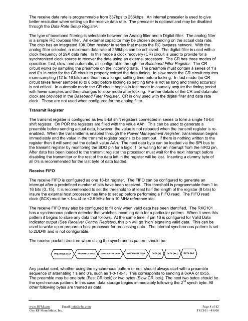
The receive data rate is programmable from 337bps to 256kbps. An internal prescaler is used to givebetter resolution when setting up the receive data rate. The prescaler is optional and may be disabledthrough the Data Rate Setup Register.The type of baseband filtering is selectable between an Analog filter and a Digital filter. The analog filteris a simple RC lowpass filter. An external capacitor may be chosen depending on the actual data rate.The chip has an integrated 10K Ohm resistor in series that makes the RC lowpass network. With theanalog filter selected, a maximum data rate of 256kbps can be achieved. The digital filter is used with aclock frequency of 29X data rate. In this mode a clock recovery (CR) circuit is used to provide for asynchronized clock source to recover the data using an external processor. The CR has three modes ofoperation: fast, slow, and automatic, all configurable through the Baseband Filter Register. The CRcircuit works by sampling the preamble on the incoming data. The preamble must contain a series of 1’sand 0’s in order for the CR circuit to properly extract the data timing. In slow mode the CR circuit requiresmore sampling (12 to 16 bits) and thus has a longer settling time before locking. In fast mode the CRcircuit takes fewer samples (6 to 8 bits) before locking so settling time is not as long and timing accuracyis not critical. In automatic mode the CR circuit begins in fast mode to coarsely acquire the timing periodwith fewer samples and then changes to slow mode after locking. Further details of the CR and data rateclock are provided in the Baseband Filter Register. CR is only used with the digital filter and data rateclock. These are not used when configured for the analog filter.Transmit RegisterThe transmit register is configured as two 8-bit shift registers connected in series to form a single 16-bitshift register. On POR the registers are filled with the value AAh. This can be used to generate apreamble before sending actual data, however, the value is not reloaded when the transmit register is reenabled.When the transmitter is enabled through the Power Management Register, transmission beginsimmediately and the value in the transmit register begins to be sent out. If there is nothing written to theregister then it will send out the default value AAh. The next data byte can be loaded via the SPI bus tothe transmit register by monitoring the SDO pin for a logic ‘1’ or waiting for an interrupt from the nIRQ pin.After data has been loaded to the transmit register the processor must wait for the next interrupt beforedisabling the transmitter or the rest of the data left in the register will be lost. Inserting a dummy byte ofall 0’s is recommended for the last byte of data loaded.Receive FIFOThe receive FIFO is configured as one 16-bit register. The FIFO can be configured to generate aninterrupt after a predefined number of bits have been received. This threshold is programmable from 1 to16 bits (0..15). It is recommended to set the threshold to at least half the length of the register (8 bits) toinsure the external host processor has time to set up before performing a FIFO read. The FIFO readclock (SCK) must be < fXTAL/4 or