TRC101 300-1000 MHz Transceiver - RF Monolithics, Inc.
TRC101 300-1000 MHz Transceiver - RF Monolithics, Inc.
TRC101 300-1000 MHz Transceiver - RF Monolithics, Inc.

Create successful ePaper yourself
Turn your PDF publications into a flip-book with our unique Google optimized e-Paper software.
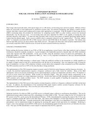
1. Pin Configuration1.1 Pin DescriptionsSDISCKnCSSDOIRQDATA/nFSELCR/FINT/FCAPCLKOUT12345678TOP VIEW<strong>TRC101</strong>161514131211109nINT/DDETRSSIAVDD<strong>RF</strong>_N<strong>RF</strong>_PGNDRESETXtal/RefPin Name Description1 SDI SPI Data In2 SCK SPI Data Clock3 nCS Chip Select Input – Selects the chip for an SPI data transaction. The pin must be pulled ‘low’ for a 16-bit read or write function. See Figure 6 for timing specifications.4 SDO SPI Data Out5 nIRQ Interrupt Request Output - The receiver will generate an active low interrupt request for themicrocontroller on the following events:· The TX register is ready to receive the next byte· The FIFO has received the preprogrammed amount of bits· Power-on reset· FIFO overflow/TX register underrun· Wake-up timer timeout· Negative pulse on the interrupt input pin nINT· Supply voltage below the preprogrammed value is detected6 Data/nFSel Data In – When the internal TX register is not used, this pin may be used to manually modulate datafrom an external host processor. If the internal TX register is enabled, this pin must be pulled “High”.When using the internal Rx FIFO, this pin must be pulled “Low” to select the FIFO. This pin is used toselect the internal registers when reading and writing.Data Out – When the internal FIFO is not used this pin is used in conjunction with pin 7 (RecoveredClock) to receive data.FIFO Select – When reading the FIFO, this pin selects the FIFO and the first bit appears on the nextclock. Use this pin in conjunction with Pin 7.7 CR/FINT/FCAP Recovered Clock Output – When the digital filter is used (Baseband Filter Register, Bit [4]) and FIFOdisabled (Configuration Register, Bit [6]), this pin provides the recovered clock from the incoming data.FIFO INT – When the internal FIFO is enabled (Configuration Register, Bit [6]), this pin acts as a FIFOFull interrupt indicating that the FIFO has filled to its pre-programmed limit (FIFO Configuration Register,Bit [7..4]).External Data Filter Capacitor – When the Analog filter is used (Baseband Filter Register, Bit [4]), thispin is the raw baseband data that may be used by a host processor for data recovery. The externalcapacitor forms a simple lowpass filter with an internal 10KOhm series resistor. The capacitor valuemay be chosen for a Max data rate up to 256kbps.8 ClkOut Optional host processor Clock Output9 Xtal/Ref Xtal - Connects to a 10<strong>MHz</strong> series crystal or an external oscillator reference. The circuit contains anintegrated load capacitor (See Configuration Register) in order to minimize the external componentcount. The crystal is used as the reference for the PLL, which generates the local oscillator frequency.The accuracy requirements for production tolerance, temperature drift and aging can be determinedfrom the maximum allowable local oscillator frequency error. Whenever a low frequency error isessential for the application, it is possible to “pull” the crystal to the accurate frequency by changing theload capacitor value.Ext Ref – An external reference, such as an oscillator, may be connected as a reference source.Connect through a .01uF capacitor.10 nRESET Reset Output with internal pull-up11 GND System Ground12 <strong>RF</strong>_P <strong>RF</strong> Diff I/O13 <strong>RF</strong>_N <strong>RF</strong> Diff I/O14 VDD Supply Voltage15 RSSIA Analog RSSI Output – The Analog RSSI can be used to determine the actual signal strength. Theresponse and settling time depends on an external filter capacitor. Typically, a <strong>1000</strong>pF capacitor willprovide optimum response time for most applications.16 nINT/DDet nINT – This pin may be configured as an active low external interrupt to the chip. When a logic ‘0’ isapplied to this pin, it causes the nIRQ pin (5) to toggle, signaling an interrupt to an external processor.Reading the first four (4) bits of the status register tells the source of the interrupt. This pin may be usedas a wake-up event from sleep.Valid Data Detector Output– This pin may be configured to indicate Valid Data when the synchronouswww.<strong>RF</strong>M.com Email: info@rfm.com Page 3 of 42©by <strong>RF</strong> <strong>Monolithics</strong>, <strong>Inc</strong>. <strong>TRC101</strong> - 4/8/08