on Cu(110) studied by STM
on Cu(110) studied by STM
on Cu(110) studied by STM

Create successful ePaper yourself
Turn your PDF publications into a flip-book with our unique Google optimized e-Paper software.
Appl. Phys. A 74, 303–305 (2002) / Digital Object Identifier (DOI) 10.1007/s003390101039<br />
Applied Physics A<br />
Materials<br />
Science & Processing<br />
Rapid communicati<strong>on</strong><br />
Growth of 3,4,9,10-perylenetetracarboxylic-dianhydride (PTCDA)<br />
<strong>on</strong> <strong>Cu</strong>(<strong>110</strong>) <strong>studied</strong> <strong>by</strong> <strong>STM</strong><br />
M. Gabriel, M. Stöhr, R. Möller ∗<br />
Universität Essen, Fachbereich Physik, Universitätsstr. 5, 45117 Essen, Germany<br />
Received: 28 September 2001/Accepted: 4 October 2001/Published <strong>on</strong>line: 20 December 2001 – © Springer-Verlag 2001<br />
Abstract. The structure of thin 3,4,9,10-perylenetetracarboxylic-dianhydride<br />
(PTCDA) films <strong>on</strong> <strong>Cu</strong>(<strong>110</strong>) was <strong>studied</strong><br />
<strong>by</strong> scanning tunnelling microscopy (<strong>STM</strong>) from subm<strong>on</strong>olayer<br />
to m<strong>on</strong>olayer coverage. While no l<strong>on</strong>g-range ordering<br />
was found after depositi<strong>on</strong> at room temperature, the formati<strong>on</strong><br />
of a well-defined superstructure is observed after thermal<br />
annealing. It appears that the formati<strong>on</strong> of the superstructure<br />
is driven <strong>by</strong> the interacti<strong>on</strong> between the oxygen atoms of the<br />
PTCDA and the copper atoms of the substrate. While the distance<br />
between the molecules fits well to the atomic lattice<br />
of the <strong>Cu</strong>(<strong>110</strong>) surface al<strong>on</strong>g the [1¯10] directi<strong>on</strong>, the mismatch<br />
al<strong>on</strong>g the [001] directi<strong>on</strong> leads to a periodic buckling<br />
normal to the surface accompanied <strong>by</strong> a restructuring of the<br />
substrate.<br />
PACS: 68.37.Ef; 68.43.Fg; 81.15.Hi<br />
During the last few years, organic semic<strong>on</strong>ductors have attracted<br />
c<strong>on</strong>siderable attenti<strong>on</strong>. Organic thin films are of interest<br />
for various applicati<strong>on</strong>s, e.g. thin insulators, sensors or<br />
light-emitting diodes (LEDs).<br />
Especially the growth of 3,4,9,10-perylenetetracarboxylic-dianhydride<br />
(PTCDA) <strong>on</strong> various substrates has become<br />
a prototype for molecular beam epitaxy with organic<br />
molecules. Surface-sensitive techniques such as scanning<br />
tunnelling microscopy (<strong>STM</strong>) and low-energy electr<strong>on</strong><br />
diffracti<strong>on</strong> (LEED) are used to characterize the thin<br />
organic films. Thin PTCDA films have been <strong>studied</strong> <strong>on</strong><br />
different substrates, such as HOPG [1, 2], Au(111) [3, 4],<br />
Au(100) [5], Ag(111) [6, 7], Ag(<strong>110</strong>) [8], GaAs(100) [9] and<br />
InAs(001) [10]. It was found that PTCDA forms well-ordered<br />
layers. In most cases, the PTCDA layers grow in the herringb<strong>on</strong>e<br />
pattern which corresp<strong>on</strong>ds to the (102) plane of the bulk<br />
crystal. So far two other formati<strong>on</strong>s of PTCDA are known. On<br />
∗ Corresp<strong>on</strong>ding author.<br />
(Fax: +41-201/183-3132, E-mail: rolf.moeller@uni-essen.de)<br />
Ag(<strong>110</strong>) the molecules form a “brickwall” structure [7] and<br />
<strong>on</strong> Au(111) a quadratic <strong>on</strong>e [4].<br />
In the present study, we report <strong>on</strong> the growth of thin layers<br />
of PTCDA <strong>on</strong> <strong>Cu</strong>(<strong>110</strong>) varying from subm<strong>on</strong>olayer to m<strong>on</strong>olayer<br />
coverage. In c<strong>on</strong>trast to the findings for other substrates,<br />
the arrangement of the PTCDA molecules is not planar but reveals<br />
a corrugati<strong>on</strong> <strong>on</strong> a large lateral scale which is attributed<br />
to periodic restructuring of the <strong>Cu</strong>(<strong>110</strong>) surface.<br />
1 Experiment<br />
The experiments were carried out in an ultrahigh-vacuum<br />
system c<strong>on</strong>sisting of different chambers for sample preparati<strong>on</strong><br />
and characterizati<strong>on</strong>. The typical base pressure is<br />
2 × 10 −10 mbar. The preparati<strong>on</strong> chamber is equipped with<br />
the standard techniques for sample cleaning. To deposit the<br />
organic molecules a small home-built crucible was used. The<br />
flow of organic molecules can be c<strong>on</strong>trolled <strong>by</strong> a quadrupole<br />
mass spectrometer. The characterizati<strong>on</strong> of the samples can<br />
be made <strong>by</strong> X-ray photoelectr<strong>on</strong> spectroscopy (XPS) and<br />
LEED, as well as <strong>by</strong> using a home-built <strong>STM</strong>, which has been<br />
optimized for operati<strong>on</strong> at low tunnelling currents of the order<br />
of a few pA.<br />
The <strong>Cu</strong>(<strong>110</strong>) surface was prepared <strong>by</strong> repeated sputtering<br />
of a copper single crystal with Ar + i<strong>on</strong>s and annealing<br />
to 790 K. The bare surface was characterized <strong>by</strong> XPS and<br />
<strong>STM</strong>. The latter measurement provided a c<strong>on</strong>venient calibrati<strong>on</strong><br />
of the <strong>STM</strong> using the known dimensi<strong>on</strong>s of the unit<br />
cell of the <strong>Cu</strong>(<strong>110</strong>) surface. The PTCDA thin films were prepared<br />
<strong>by</strong> evaporati<strong>on</strong> from a crucible at a temperature of<br />
480 K while the substrate was kept at room temperature. For<br />
the preparati<strong>on</strong> of the subm<strong>on</strong>olayer and m<strong>on</strong>olayer, a rate<br />
of 0.5ML/min was chosen. Afterwards, the films were thermally<br />
annealed using a linear temperature ramp of 1 K/s,<br />
ending at 450 K. During the annealing it was to be c<strong>on</strong>trolled<br />
<strong>by</strong> the mass spectrometer if desorpti<strong>on</strong> of the PTCDA<br />
molecules from the <strong>Cu</strong> surface took place. However, no desorpti<strong>on</strong><br />
from the sample was detected.
304<br />
2 Results and discussi<strong>on</strong><br />
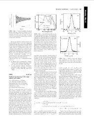
Figure 1 shows an image of the clean <strong>Cu</strong>(<strong>110</strong>) single crystal.<br />
The individual atoms are clearly resolved. The crystallographic<br />
directi<strong>on</strong>s are readily identified, as indicated <strong>by</strong> the<br />
arrows. The orientati<strong>on</strong> of the substrate was maintained during<br />
the following experiments.<br />
Figure 2 shows a typical image of PTCDA <strong>on</strong> <strong>Cu</strong>(<strong>110</strong>)<br />
at a coverage of about 0.6 ML immediately after depositi<strong>on</strong><br />
of the molecules. Since the substrate was kept at room temperature,<br />
the mobility of the molecules was relatively low. In<br />
c<strong>on</strong>sequence they showed a tendency to cluster, but no l<strong>on</strong>grange<br />
order was found. Apparently the molecules are lying<br />
flat <strong>on</strong> the copper substrate. The latter was not modified <strong>by</strong> the<br />
adsorpti<strong>on</strong>.<br />
After thermal annealing to 450 K the same sample displayed<br />
a very striking feature, as shown in Fig. 3. The<br />
molecules formed stripes with a significant corrugati<strong>on</strong>. Since<br />
no desorpti<strong>on</strong> could be detected during the annealing, the<br />
coverage equals that in Fig. 2. It can be clearly seen that the<br />
molecules have rearranged themselves into islands with a<br />
dense packing. They are found preferentially at step edges.<br />
Figure 4 shows the arrangement of the molecules in more<br />
detail. The superstructure essentially follows a rectangular<br />
pattern which has the same orientati<strong>on</strong> as the unit cell of the<br />
substrate. However it is not simply a commensurate structure.<br />
Al<strong>on</strong>g the [1¯10] directi<strong>on</strong> the ordering follows a clear<br />
scheme. Two molecules form the base, which extends over<br />
10 copper atoms. Every sec<strong>on</strong>d molecule is rotated <strong>by</strong> 90 ◦ .<br />
Figure 5 shows several line scans al<strong>on</strong>g this directi<strong>on</strong>.<br />
The situati<strong>on</strong> is more complicated for the [001] directi<strong>on</strong>.<br />
Again every sec<strong>on</strong>d molecule is rotated <strong>by</strong> 90 ◦ ; however,<br />
since the distance between the atomic rows is √ 2 times larger<br />
than in the [1¯10] directi<strong>on</strong>, there is no accidental match of the<br />
spacing of the molecules and the substrate atoms for a flat arrangement<br />
of the molecules. It appears that the tendency of<br />
the molecules to lock in specific positi<strong>on</strong>s <strong>on</strong> the substrate is<br />
so str<strong>on</strong>g that it causes a large-scale restructuring of the substrate<br />
<strong>by</strong> additi<strong>on</strong> or removal of atomic rows al<strong>on</strong>g the [1¯10]<br />
Fig. 1. Atomically resolved image of the <strong>Cu</strong>(<strong>110</strong>) surface, 5 × 5nm 2 ,the<br />
tunnelling parameters are U t =−0.4 V (at the tip) and I t =−225 pA<br />
Fig. 3. <strong>STM</strong> image of the sample after annealing to 450 K; the area is 100×<br />
90 nm 2 ; the tunnelling parameters are U t = 2.1Vand I t = 2pA<br />
Fig. 2. <strong>STM</strong> image of a fracti<strong>on</strong> of a m<strong>on</strong>olayer of PTCDA <strong>on</strong> <strong>Cu</strong>(<strong>110</strong>)<br />
before annealing; the area is 180 × 80 nm 2 ; the tunnelling parameters are<br />
U t =−0.8Vand I t = 3pA<br />
Fig. 4. <strong>STM</strong> image of the smaller area of the sample after annealing,<br />
theareais10× 8nm 2 ; the tunneling parameters are U t =−0.45 V and<br />
I t = 300 pA
305<br />
0.10<br />
0,05<br />
0,00<br />
−0,05<br />
−0,10<br />
Fig. 5. Cross-secti<strong>on</strong>s al<strong>on</strong>g the [1¯10] directi<strong>on</strong><br />
directi<strong>on</strong>. As a result a corrugati<strong>on</strong> is found which has a periodicity<br />
of either four, five or six molecular rows. Figure 6<br />
shows several line scans to illustrate the situati<strong>on</strong>. The largescale<br />
corrugati<strong>on</strong> amounts to 0.18 nm, which is the distance<br />
between adjacent layers of the <strong>Cu</strong>(<strong>110</strong>) substrate.<br />
For several reas<strong>on</strong>s we rule out the idea that the corrugati<strong>on</strong><br />
is due to the formati<strong>on</strong> of a sec<strong>on</strong>d layer of PTCDA<br />
molecules which might lead to a similar difference in height.<br />
First of all, if <strong>on</strong>e compares the relative porti<strong>on</strong> of the surface<br />
which is not covered <strong>by</strong> molecules before and after thermal<br />
annealing, it is found to remain unchanged. However, if a sec<strong>on</strong>d<br />
layer were partially formed, the uncovered surface should<br />
increase. Sec<strong>on</strong>d, the molecules between the upper and the<br />
lower regi<strong>on</strong>s appear to be tilted, which is not expected for a<br />
step to the next molecular layer. The observati<strong>on</strong> is independent<br />
of tunnelling voltage and current. Hence, the idea that it<br />
is due to an effect of the electr<strong>on</strong>ic structure may be excluded.<br />
If the coverage is increased to <strong>on</strong>e m<strong>on</strong>olayer, the superstructure<br />
discussed above expands all over the surface.<br />
Figure 7 shows a m<strong>on</strong>olayer of PTCDA after annealing to<br />
450 K.<br />
The presented superstructure differs from those found so<br />
far <strong>on</strong> other substrates. For many substrates the “herringb<strong>on</strong>e”<br />
structure is found which is equivalent to the (102) plane<br />
of the PTCDA bulk. The reported ordering represents the<br />
first example of a n<strong>on</strong>-planar superstructure of PTCDA. Furthermore,<br />
it induces a restructuring of the substrate which<br />
is accompanied <strong>by</strong> a massive transport of substrate atoms.<br />
0,70<br />
0,65<br />
0,60<br />
0,55<br />
0,50<br />
0,45<br />
0,40<br />
0,35<br />
0,30<br />
0,25<br />
0,20<br />
0,15<br />
0,10<br />
0,05<br />
0,00<br />
Fig. 6. Cross-secti<strong>on</strong>s al<strong>on</strong>g the [001] directi<strong>on</strong><br />
Fig. 7. <strong>STM</strong> image of about <strong>on</strong>e m<strong>on</strong>olayer of PTCDA <strong>on</strong> <strong>Cu</strong>(<strong>110</strong>),<br />
annealed to 450 K; the area is 91 × 87 nm 2 ; the tunnelling parameters are<br />
U t = 2.6Vand I t = 2pA<br />
A similar case of surface restructuring induced <strong>by</strong> organic<br />
molecules has been reported for C 60 <strong>on</strong> Ni(<strong>110</strong>) [11].<br />
3 Summary<br />
The growth of thin films of PTCDA <strong>on</strong> <strong>Cu</strong>(<strong>110</strong>) was <strong>studied</strong><br />
<strong>by</strong> <strong>STM</strong> in UHV. The ordering of the molecules is commensurate<br />
al<strong>on</strong>g the [1¯10] directi<strong>on</strong>, leading to a perfectly<br />
regular pattern. However, there is a mismatch between the<br />
intermolecular distances and the atomic distances of the unrec<strong>on</strong>structed<br />
<strong>Cu</strong>(<strong>110</strong>) surface al<strong>on</strong>g the [001] directi<strong>on</strong>. In<br />
c<strong>on</strong>necti<strong>on</strong> with the str<strong>on</strong>g interacti<strong>on</strong> between the molecules<br />
and the substrate, this leads to a rearrangement of the atomic<br />
rows of the substrate, resulting in a quasi-periodic corrugati<strong>on</strong><br />
of 0.18 nm, which equals the height of a m<strong>on</strong>o-atomic step.<br />
The ordering exhibits some variati<strong>on</strong>; the periodicity varies<br />
between four and six molecular rows.<br />
Acknowledgements. We would like to thank Prof. Dr. N. Karl for fruitful<br />
discussi<strong>on</strong>s. This work was supported <strong>by</strong> the Deutsche Forschungsgemeinschaft<br />
(S<strong>on</strong>derforschungsbereich SFB 452).<br />
References<br />
1. B. Uder, C. Ludwig, J. Petersen, B. Gompf, W. Eisenmenger: Z. Phys.<br />
B 97, 389 (1995)<br />
2. C. Kendrick, A. Kahn, S.R. Forrest: Appl. Surf. Sci. 104, 586<br />
(1996)<br />
3. T. Schmitz-Hübsch, T. Fritz, F. Sellam, R. Staub, K. Leo: Phys. Rev. B<br />
55, 7972 (1996)<br />
4. I. Chizhov, A. Kahn, G. Scoles: J. Crystal Growth 208, 449 (2000)<br />
5. T. Schmitz-Hübsch, T. Fritz, R. Staub, A. Back, N.R. Armstr<strong>on</strong>g,<br />
K. Leo: Surf. Sci. 437, 163 (1999)<br />
6. E. Umbach, K. Glöckler, M. Sokolowski: Surf. Sci. 402, 20 (1998)<br />
7. K. Glöckler, C. Seidel, A. Soukopp, M. Sokolowski, E. Umbach,<br />
M. Böhringer, R. Berndt, W.-D. Schneider: Surf. Sci. 405, 1 (1998)<br />
8. C. Seidel, C. Awater, X.D. Liu, R. Ellerbrake, H. Fuchs: Surf. Sci. 371,<br />
123 (1997)<br />
9. C. Kendrick, A. Kahn: Surf. Rev. Lett. 5, 289 (1998)<br />
10. C. Kendrick, A. Kahn: Appl. Surf. Sci. 123, 405 (1998)<br />
11. P.W. Murray, M.O. Pedersen, E. Lægsgaard, I. Stensgaard, F. Besenbacher:<br />
Phys. Rev. B 55, 9360 (1997)