On the annealing mechanism of AuGe/Ni/Au ohmic contacts to a two ...
On the annealing mechanism of AuGe/Ni/Au ohmic contacts to a two ...
On the annealing mechanism of AuGe/Ni/Au ohmic contacts to a two ...

Create successful ePaper yourself
Turn your PDF publications into a flip-book with our unique Google optimized e-Paper software.
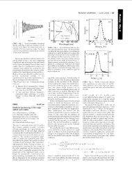
Semicond. Sci. Technol. 28 (2013) 025006however, that <strong>the</strong> required cleaning depends on <strong>the</strong> amount <strong>of</strong>surface adhesives and contaminants at <strong>the</strong> start <strong>of</strong> <strong>the</strong> process.Insufficient cleaning gives higher contact resistance values andprohibits reproducibility.3. Electrical measurementsWe measured <strong>the</strong> current–voltage (IV) characteristics <strong>of</strong> all<strong>contacts</strong> <strong>to</strong> determine optimal <strong>annealing</strong> parameters. We foundthat a suitable and sufficient definition for an optimal <strong>ohmic</strong>contact is a contact with <strong>the</strong> lowest zero-bias resistance at4.2 K. The typical resistance for such a contact is ∼20 ,but we have observed resistances as low as 5 . These valuesfor contact resistance are close <strong>to</strong> <strong>the</strong> lowest values that havebeen reported 3 . All <strong>contacts</strong> defined as optimal in this mannershowed highly linear IVs up <strong>to</strong> at least 1 mV (over and underannealed <strong>contacts</strong> did show nonlinear IVs due <strong>to</strong> effects suchas Schottky or tunnel barriers in <strong>the</strong> <strong>contacts</strong>). Fur<strong>the</strong>rmore, all<strong>the</strong>se optimal <strong>contacts</strong> showed a strong mono<strong>to</strong>nous reduction<strong>of</strong> <strong>the</strong> contact resistance upon lowering <strong>the</strong> sample temperaturefrom 300 <strong>to</strong> 4.2 K. Highly over and under annealed <strong>contacts</strong>showed an increase <strong>of</strong> <strong>the</strong> contact resistance upon cooling <strong>to</strong>4.2 K.We used a current-biased four-terminal configuration <strong>to</strong>measure <strong>the</strong> voltage drop across a single contact. The goalhere was <strong>to</strong> obtain a good value for <strong>the</strong> resistance between<strong>the</strong> surface metalization <strong>of</strong> a contact and 2DEG right next<strong>to</strong> a contact. Thus, we connect one current terminal and onevoltage terminal <strong>to</strong> <strong>the</strong> low-resistance bond wire that is pressedon <strong>the</strong> surface metalization. The o<strong>the</strong>r current terminal andvoltage terminal are attached <strong>to</strong> <strong>two</strong> different <strong>ohmic</strong> <strong>contacts</strong>right next <strong>to</strong> <strong>the</strong> contact that is investigated (this allowed us<strong>to</strong> use a standard sample design in our fabrication facility).We accounted for a small voltage drop in <strong>the</strong> 2DEG areabetween <strong>the</strong> investigated contact and <strong>the</strong> voltage probe via<strong>the</strong> 2DEG. We are aware that <strong>the</strong> transmission line method(TLM) [28, 29] is a better method for determining <strong>the</strong> exactvalue <strong>of</strong> a contact resistance, but this is not needed forour approach. We compare resistances <strong>of</strong> various annealed<strong>contacts</strong> that were fabricated under identical conditions besides<strong>the</strong> variation in <strong>annealing</strong> time and temperature. Within sucha set, we determine which <strong>contacts</strong> have <strong>the</strong> lowest contactresistance. When reproducing our results with <strong>contacts</strong> thatwere fabricated in a different batch (using <strong>the</strong> same electronbeamevapora<strong>to</strong>r, but after replenishing <strong>the</strong> <strong><strong>Au</strong>Ge</strong> target), wefind that <strong>the</strong> values <strong>of</strong> <strong>the</strong> lowest contact resistance can bedifferent up <strong>to</strong> a fac<strong>to</strong>r 2 around <strong>the</strong> typical result. We attribute<strong>the</strong>se batch-<strong>to</strong>-batch fluctuations <strong>to</strong> variations in <strong>the</strong> exactcomposition <strong>of</strong> <strong>the</strong> <strong><strong>Au</strong>Ge</strong>/<strong>Ni</strong>/<strong>Au</strong> layer that we deposit, andpossibly due <strong>to</strong> <strong>the</strong> dependence <strong>of</strong> results on how well <strong>the</strong>3 The work that we cite in <strong>the</strong> introduction shows that <strong>the</strong> lowest values forcontact resistance <strong>to</strong> n-GaAs and 2DEG systems with only a thin (few nm)buffer layer (undoped Al x Ga 1−x As between doping and <strong>the</strong> 2DEG) are <strong>of</strong> order0.1 mm, giving 0.5 for 0.2 mm wide <strong>contacts</strong>. However, 2DEG systemswith <strong>the</strong> thickness <strong>of</strong> <strong>the</strong> buffer layer in <strong>the</strong> range <strong>of</strong> 35 nm typically give valuesthat are an order <strong>of</strong> magnitude higher [22]. Note that values are <strong>of</strong>ten reportedin units mm, which is not representing <strong>the</strong> bulk resistivity between surfacemetalization and 2DEG, but representing <strong>the</strong> contact resistance normalized <strong>to</strong>contact width, as derived with <strong>the</strong> TLM method [28, 29].E J Koop et alsurface cleaning before processing worked out. The optimal<strong>annealing</strong> times, however, show batch-<strong>to</strong>-batch fluctuations <strong>of</strong>only 10%. Thus, our approach <strong>to</strong> determine optimal <strong>annealing</strong>conditions does not depend on <strong>the</strong> exact value <strong>of</strong> <strong>the</strong> measuredcontact resistance.Figure 1(b) shows a typical result, from which wedetermine <strong>the</strong> optimal <strong>annealing</strong> time for <strong>contacts</strong> <strong>to</strong> waferC for <strong>the</strong> case <strong>of</strong> <strong>annealing</strong> with <strong>the</strong> oven at 450 ◦ C 4 . Contactresistance data that is denoted as 〈R〉 is <strong>the</strong> average resistancemeasured on a set <strong>of</strong> eight identical <strong>contacts</strong>, and <strong>the</strong> error barrepresents <strong>the</strong> standard deviation. The results in figure 1(b)show a clear minimum in contact resistance for <strong>annealing</strong>times near 5 min. We fit a parabola (phenomenological ansatz)<strong>to</strong> <strong>the</strong> log〈R〉 values <strong>of</strong> <strong>the</strong>se data points, and define <strong>the</strong> optimal<strong>annealing</strong> time as <strong>the</strong> time coordinate <strong>of</strong> <strong>the</strong> minimum <strong>of</strong> <strong>the</strong>parabola. In this manner, <strong>the</strong> optimal <strong>annealing</strong> times t A,Opt areobtained for <strong>contacts</strong> on wafers A, B and C annealed at each<strong>of</strong> <strong>the</strong> temperatures.Figure 1(c) presents <strong>the</strong>se optimal <strong>annealing</strong> times.As expected, <strong>the</strong> optimal <strong>annealing</strong> time increases as <strong>the</strong>temperature is decreased, and increases as <strong>the</strong> depth d <strong>of</strong> <strong>the</strong>2DEG increases. While it is known that several simultaneousdiffusion processes play a role in contact formation [9], wewill, for <strong>the</strong> sake <strong>of</strong> argument, show that a simple diffusionmodel has little value for predicting how optimal <strong>annealing</strong>times depend on <strong>the</strong> depth d and <strong>the</strong> <strong>annealing</strong> temperature.For this simple diffusion model, we assume that a certaindopant (with fixed concentration C 0 at <strong>the</strong> surface) diffusesin<strong>to</strong> <strong>the</strong> heterostructure. The relevant solution <strong>to</strong> Fick’s secondlaw is <strong>the</strong>nzC = C 0 erfc√ . (1)4DtHere C is <strong>the</strong> doping concentration at time t and depth zin<strong>to</strong> <strong>the</strong> heterostructure, and D is <strong>the</strong> diffusion constant (erfcis complementary error function). Since <strong>the</strong> temperature <strong>of</strong>our sample is not constant (see figure 1(a)) we will use <strong>the</strong>measured temperature pr<strong>of</strong>ile T(t) <strong>to</strong> integrate <strong>the</strong> diffusionconstant over time, and use in equation (1) ∫ D(t)dt instead <strong>of</strong>Dt, where(D(t) = D 0 exp − E )a, (2)k B T(t)and where E a is an activation energy. We assume that anoptimal contact <strong>the</strong>n always occurs for a certain optimal valuefor C/C 0 at <strong>the</strong> depth <strong>of</strong> <strong>the</strong> 2DEG (z = d). We define <strong>the</strong><strong>annealing</strong> time as <strong>the</strong> time from start <strong>to</strong> <strong>the</strong> moment when<strong>the</strong> boat is taken out <strong>of</strong> <strong>the</strong> oven, but integrate over <strong>the</strong> entiretime span that <strong>the</strong> sample is at elevated temperatures, (as shownin figure 1(a), fully including <strong>the</strong> cooling down). This gives4 In figure 1(b), we plot <strong>the</strong> contact resistance as a function <strong>of</strong> <strong>annealing</strong>time t A (and derived from that, we use t A,Opt in figures 1(c) and 3(c)). Fortransferring our results <strong>to</strong> o<strong>the</strong>r <strong>annealing</strong> setups (that can have different timeconstants for <strong>the</strong> heating and cooling process), <strong>the</strong> relevant quantity is in fact<strong>the</strong> integrated diffusion. We still choose <strong>to</strong> present results as a function <strong>of</strong> t Asince our estimate for <strong>the</strong> integrated diffusion has a much larger error bar.The plot figure 1(a) can be used for estimating <strong>the</strong> integrated diffusion andtransferring it <strong>to</strong> <strong>the</strong> heating curve <strong>of</strong> ano<strong>the</strong>r setup. The overall behavior <strong>of</strong>our model should <strong>the</strong>n remain valid for setups with similar timescales for <strong>the</strong>heating and cooling process.3
Semicond. Sci. Technol. 28 (2013) 025006E J Koop et ala model with <strong>the</strong> activation energy E a , diffusion constant D 0and concentration C/C 0 as fitting parameters.The gray lines in figure 1(c) show <strong>the</strong> best fitting result thatreasonably covers all nine data points in a single fit. Besides <strong>the</strong>fact that <strong>the</strong> shape <strong>of</strong> <strong>the</strong> traces only poorly matches <strong>the</strong> trendin <strong>the</strong> data, <strong>the</strong> parameter values give unreasonable results.The temperature dependence alone governs <strong>the</strong> fitting resultfor E a , giving here 0.15 eV. This is on <strong>the</strong> low side for typicalvalues for diffusion in GaAs materials (∼1 eV) [30–32]. Forfixed E a , various combinations <strong>of</strong> C/C 0 and D 0 give identicalresults. When assuming a typical value D 0 ∼ 3×10 −7 m 2 s −1(for diffusion <strong>of</strong> Ge, <strong>Ni</strong> or <strong>Au</strong> in GaAs [30–32]), this fit yieldsC/C 0 very close <strong>to</strong> 1, i.e. completely saturated diffusion. Thisis in contradiction with <strong>the</strong> clear dependence on depth that weobserve (and this remains <strong>the</strong> case when allowing for E a up<strong>to</strong> ∼1 eV, but <strong>the</strong>n <strong>the</strong> fit does not cover all nine data pointsat all). Thus, we find that predicting optimal <strong>annealing</strong> timeswith simple diffusion (according <strong>to</strong> t A,Opt ∝ d 2 at constanttemperature) does not work and that a more complex modelneeds <strong>to</strong> be considered.(a)500 nm(c)2DEG(d )2DEG(b)2DEG<strong>Ni</strong>,Ge<strong>Au</strong>AlGaAsOriginalwafer surfaceGaAsSuperlatticeGaAs500 nm500 nm4. TEM and EDX resultsWe have studied <strong>the</strong> contact formation using cross-sectionalTEM imaging <strong>of</strong> <strong>contacts</strong> at several stages during <strong>the</strong> <strong>annealing</strong>process. The samples were prepared for TEM imaging by usinga focused ion beam (FIB) <strong>to</strong> slice out a micrometer thin piece<strong>of</strong> <strong>the</strong> measured contact. By fur<strong>the</strong>r thinning using <strong>the</strong> FIB <strong>the</strong>thickness was reduced <strong>to</strong> 100 nm.Figure 2(a) shows an overview <strong>of</strong> an optimally annealedcontact on wafer C which was annealed for 5 min at 450 ◦ C.The composition <strong>of</strong> <strong>the</strong> various phases has been determinedby energy dispersive x-ray (EDX) analysis and is illustratedin figure 2(b). From bot<strong>to</strong>m <strong>to</strong> <strong>to</strong>p, we recognize <strong>the</strong> GaAssubstrate, and an AlAs/GaAs superlattice <strong>to</strong> smoo<strong>the</strong>n <strong>the</strong>surface <strong>of</strong> <strong>the</strong> substrate. <strong>On</strong> <strong>to</strong>p <strong>of</strong> that we find ano<strong>the</strong>r layer<strong>of</strong> epitaxially grown GaAs and a layer <strong>of</strong> Al x Ga 1−x As. The2DEG is at <strong>the</strong> interface <strong>of</strong> <strong>the</strong>se <strong>two</strong> layers. The GaAs cappinglayer that was originally on <strong>to</strong>p <strong>of</strong> <strong>the</strong> Al x Ga 1−x As layer is nolonger visible. Instead, we see large <strong>Au</strong>-rich and <strong>Ni</strong>-rich grainsthat have penetrated below <strong>the</strong> original wafer surface. Both <strong>of</strong><strong>the</strong>se phases contain out-diffused Ga and As, with Ga mainlyin <strong>the</strong> <strong>Au</strong>-rich grains and As mainly in <strong>the</strong> <strong>Ni</strong>-rich grains.Fur<strong>the</strong>rmore, <strong>the</strong> <strong>Ni</strong>-rich phase absorbed most <strong>of</strong> <strong>the</strong> Ge. Wefind that <strong>the</strong> <strong>Au</strong> grains do not contain any Ge, consistent with<strong>the</strong> findings <strong>of</strong> Kuan et al [9] in work with n-GaAs.The wide and curved dark lines going over all <strong>the</strong>heterostructure layers (most clearly visible in <strong>the</strong> GaAs layers)are due <strong>to</strong> strain induced by <strong>the</strong> FIB sample preparation andare not related <strong>to</strong> <strong>the</strong> diffusion process.We find that <strong>the</strong> <strong>Au</strong>-rich and <strong>Ni</strong>-rich grains do not have<strong>to</strong> penetrate <strong>the</strong> 2DEG in order <strong>to</strong> establish a good electricalcontact. We can rule out that we do not see grains reaching <strong>the</strong>2DEG due <strong>to</strong> <strong>the</strong> small thickness <strong>of</strong> <strong>the</strong> sample slice, since weobserved no substantial variation in <strong>the</strong> penetration depth <strong>of</strong> alarge number <strong>of</strong> <strong>Au</strong> and <strong>Ni</strong> grains going along <strong>the</strong> sample slice.We examined <strong>two</strong> slices from <strong>two</strong> different samples, both withFigure 2. (a) Cross-section TEM image <strong>of</strong> a contact on wafer C,annealed for <strong>the</strong> optimal <strong>annealing</strong> time at 450 ◦ C. (b) A sketch <strong>of</strong><strong>the</strong> TEM image in (a) <strong>to</strong> specify <strong>the</strong> various layers and phases. (c)Larger area TEM image <strong>of</strong> <strong>the</strong> same contact as in (a) showing large<strong>Au</strong>-rich (black) and <strong>Ni</strong>-rich grains (dark gray) contacting <strong>the</strong>Al x Ga 1−x As. (d) Similar image for a highly over annealed contact.The <strong>Au</strong> and <strong>Ni</strong> grains still do not penetrate <strong>the</strong> 2DEG, but <strong>Au</strong> hasdiffused underneath <strong>the</strong> <strong>Ni</strong> grains, which results in an increasedcontact resistance.a length <strong>of</strong> 100 µm, after electrical measurements confirmedthat <strong>the</strong>se <strong>contacts</strong> were indeed optimally annealed.The TEM image in figure 2(c) shows a larger region <strong>of</strong> anoptimally annealed contact. Large <strong>Au</strong> and <strong>Ni</strong> grains that havepenetrated <strong>the</strong> Al x Ga 1−x As layer can be identified. Figure 2(d)shows an over annealed contact on wafer C, that was annealedfor 7 min at 450 ◦ C. Remarkably, <strong>the</strong> <strong>Au</strong> and <strong>Ni</strong> grains did notpenetrate much fur<strong>the</strong>r in<strong>to</strong> <strong>the</strong> Al x Ga 1−x As and do still notreach <strong>the</strong> 2DEG 5 . The most significant change with respect t<strong>of</strong>igure 2(c) is that <strong>the</strong> <strong>Au</strong>-rich phase is diffusing underneath<strong>the</strong> <strong>Ni</strong>-rich grains, reducing <strong>the</strong> <strong>to</strong>tal <strong>Ni</strong>-grain–Al x Ga 1−x Asinterface area. This was also observed by Kuan et al [9](and confirmed in detailed studies by Lumpkin et al [18]) inwork on n-GaAs, and <strong>the</strong> results <strong>of</strong> <strong>the</strong>se authors indicate thatthis process is mainly responsible for <strong>the</strong> increase in contactresistance when a sample is being over annealed.Kuan et al [9] report that <strong>the</strong> contact resistance issensitive <strong>to</strong> <strong>the</strong> ratio <strong>of</strong> <strong>the</strong> <strong>to</strong>tal contact area between <strong>Au</strong>richregions and Al x Ga 1−x As and that <strong>of</strong> <strong>Ni</strong>-rich regions.The <strong>Au</strong>–Al x Ga 1−x As interface is considered a region <strong>of</strong> poorconductance because <strong>the</strong> <strong>Au</strong>-rich grains (in contrast <strong>to</strong> <strong>Ni</strong>-richgrains) do not contain any Ge, such that it cannot act as asource for diffusion <strong>of</strong> Ge in<strong>to</strong> <strong>the</strong> heterostructure. However,5 While we do not have TEM images <strong>of</strong> optimal <strong>contacts</strong> <strong>of</strong> wafer A (depth<strong>of</strong> 2DEG at 70 nm), we use <strong>the</strong> results <strong>of</strong> figures 2(c) and (d) (from wafer C,with metal grains penetrating till 70 and 90 nm, respectively) <strong>to</strong> estimate thatfor optimal <strong>contacts</strong> <strong>of</strong> wafer A <strong>the</strong> metal grains also do not reach <strong>the</strong> 2DEGdepth.4
Semicond. Sci. Technol. 28 (2013) 025006it is <strong>to</strong> our knowledge not yet unders<strong>to</strong>od why <strong>the</strong> diffusion <strong>of</strong><strong>Au</strong> underneath <strong>the</strong> <strong>Ni</strong> grains at later stages <strong>of</strong> <strong>annealing</strong> (whena large amount <strong>of</strong> Ge already diffused out <strong>of</strong> <strong>Ni</strong>) results in astrong increase <strong>of</strong> <strong>the</strong> contact resistance.5. Summary <strong>of</strong> <strong>annealing</strong> <strong>mechanism</strong>In this section, we use <strong>the</strong> results from <strong>the</strong> previous <strong>two</strong>sections, <strong>to</strong>ge<strong>the</strong>r with established results from <strong>the</strong> literature,for giving a qualitative description <strong>of</strong> <strong>the</strong> formation <strong>of</strong> an <strong>ohmic</strong>contact <strong>to</strong> a 2DEG in a GaAs/Al x Ga 1−x As heterostructure. It isremarkably similar <strong>to</strong> <strong>the</strong> <strong>annealing</strong> <strong>mechanism</strong> as describedby Kuan et al [9] for <strong>contacts</strong> <strong>to</strong> n-GaAs. In <strong>the</strong> initial stages<strong>of</strong> <strong>the</strong> <strong>annealing</strong> process (already during <strong>the</strong> heating <strong>of</strong> <strong>the</strong>sample) <strong>Au</strong> and Ge segregate, and most Ge forms a newphase with <strong>the</strong> <strong>Ni</strong>. At <strong>the</strong> same time, <strong>the</strong>se Ge-rich <strong>Ni</strong> grainsmove <strong>to</strong> <strong>the</strong> wafer surface due <strong>to</strong> a wetting effect [16], whichresults in <strong>the</strong> situation that <strong>the</strong> wafer surface is covered withneighboring <strong>Au</strong> and <strong>Ni</strong> x Ge 6 grains. There is evidence thatfor thin metalization layers (∼100 nm) this process alreadyoccurs well below <strong>the</strong> bulk melting temperature (363 ◦ C) <strong>of</strong><strong>the</strong> eutectic <strong><strong>Au</strong>Ge</strong> phase [16].Next, at higher temperatures, both <strong>the</strong> <strong>Au</strong>-rich and<strong>Ni</strong>-rich grains penetrate in<strong>to</strong> <strong>the</strong> heterostructure by solidphase inter-diffusion, compensated by a back flow <strong>of</strong> Asand Ga. Our EDX results confirm that Ga mainly flows in<strong>to</strong><strong>Au</strong>, and As mainly in<strong>to</strong> <strong>Ni</strong>-rich grains. This concerns <strong>the</strong>formation <strong>of</strong> new material phases. In several earlier studies[9, 19, 12, 14, 16–18] <strong>the</strong>se phases have been identified as<strong>Au</strong>Ga alloys and phases close <strong>to</strong> <strong>Ni</strong> 2 GeAs. These phasespenetrate only tens <strong>of</strong> nm below <strong>the</strong> original wafer surfacefor typical <strong>annealing</strong> conditions [9, 14].At <strong>the</strong> same time, <strong>the</strong>re is diffusion <strong>of</strong> a<strong>to</strong>mic Ge, <strong>Ni</strong> and<strong>Au</strong> (at similar concentrations) in<strong>to</strong> <strong>the</strong> heterostructure, whichpenetrates deeper [8, 19, 20, 15, 27]. In particular, Ge diffusesout <strong>of</strong> <strong>the</strong> <strong>Ni</strong>-rich grains in<strong>to</strong> <strong>the</strong> Al x Ga 1−x As layers, and agood <strong>ohmic</strong> contact is formed when <strong>the</strong> Al x Ga 1−x As layersare sufficiently doped with Ge all <strong>the</strong> way up <strong>to</strong> <strong>the</strong> 2DEG.While this is progressing, <strong>the</strong> <strong>Au</strong>-rich grains start <strong>to</strong> expandunderneath <strong>the</strong> <strong>Ni</strong>-rich grains [9, 18], which have <strong>the</strong> lowestcontact resistance with <strong>the</strong> doped Al x Ga 1−x As layer since <strong>the</strong>ywere <strong>the</strong> dominant supplier <strong>of</strong> Ge. The expansion <strong>of</strong> <strong>the</strong> <strong>Au</strong>Gagrains is possibly due <strong>to</strong> <strong>the</strong> relatively low activation energyfor out diffusion <strong>of</strong> Ga in<strong>to</strong> <strong>Au</strong> [32] (while <strong>the</strong> Al–As bindingenergy is relatively high [19]). This latter process increases <strong>the</strong>interface resistance between <strong>the</strong> metalization on <strong>the</strong> surfaceand <strong>the</strong> doped Al x Ga 1−x As layer. Thus, <strong>the</strong> formation <strong>of</strong> anoptimal contact is a competition between <strong>the</strong>se <strong>two</strong> processes.The in-diffusion <strong>of</strong> Ge lowers <strong>the</strong> contact resistance for<strong>two</strong> reasons. (1) The full Al x Ga 1−x As region between <strong>the</strong>surface and <strong>the</strong> 2DEG becomes a highly doped region with areasonably low bulk resistivity. (2) The Ge doping in this regionmakes <strong>the</strong> Schottky barrier between <strong>the</strong> doped semiconduc<strong>to</strong>rand <strong>the</strong> surface metalization very thin (<strong>the</strong> barrier height is6 Early in <strong>the</strong> <strong>annealing</strong> process, <strong>the</strong> grains mainly containing <strong>Ni</strong> and Ge havebeen identified as <strong>Ni</strong>Ge, <strong>Ni</strong> 2 Ge and <strong>Ni</strong> 3 Ge phases [9, 12].E J Koop et alprobably not changing significantly 7 ), up <strong>to</strong> <strong>the</strong> point where itsseries contribution <strong>to</strong> <strong>the</strong> contact resistance is small. The <strong>to</strong>talcontact resistance is <strong>the</strong>n dominated by doped Al x Ga 1−x Asregion, giving linear transport characteristics (a similar effec<strong>to</strong>ccurs for <strong>contacts</strong> <strong>to</strong> n-GaAs due <strong>to</strong> spreading resistancebelow <strong>the</strong> contact [6]).As said, it is not yet well established which processes areresponsible for <strong>the</strong> resistance increase upon over <strong>annealing</strong>.The fact that over <strong>annealing</strong> with 2DEG samples and n-GaAssamples [9] occurs qualitatively in a very similar manner (andalso at similar <strong>annealing</strong> times and temperatures) is a firstindication that it is due <strong>to</strong> a process near <strong>the</strong> interface withmetal-rich phases on <strong>the</strong> surface, ra<strong>the</strong>r than a process at <strong>the</strong>depth <strong>of</strong> <strong>the</strong> 2DEG or <strong>the</strong> edge <strong>of</strong> a contact. Fur<strong>the</strong>rmore,our results now show that <strong>the</strong> resistance increase for 2DEGsamples is also correlated with <strong>the</strong> expanding <strong>Au</strong>Ga grainsbelow <strong>the</strong> <strong>Ni</strong>-rich grains. Various authors have suggested that<strong>the</strong> increasing contact resistance that is associated with over<strong>annealing</strong> may be due <strong>to</strong> a large number <strong>of</strong> vacancies justbelow <strong>the</strong> metal-rich phases near <strong>the</strong> surface [19, 14, 24](but o<strong>the</strong>rs suggested it was due <strong>to</strong> excessive in-diffusion <strong>of</strong><strong>Ni</strong> [5, 14]). These mainly result from out-diffusion <strong>of</strong> Gain<strong>to</strong> <strong>the</strong> <strong>Au</strong>-rich grains (which indeed results in a very stable<strong>Au</strong>Ga phase near <strong>the</strong> original wafer surface [5, 16, 17]). Thesevacancies occur in particular when <strong>the</strong>re is no (longer) Gediffusion in<strong>to</strong> <strong>the</strong>se vacancies. <strong>On</strong>e should note, however,that with n-GaAs an increasing contact resistance was alsoobserved without an expansion <strong>of</strong> <strong>the</strong> <strong>Au</strong>Ga grains below <strong>the</strong><strong>Ni</strong>-rich grains [14], but this does not rule out that an increasingnumber <strong>of</strong> vacancies is responsible for over <strong>annealing</strong>.Finally, we remark that both <strong>the</strong> <strong>Ni</strong>-rich and <strong>Au</strong>-rich grainsare probably important for rapid <strong>annealing</strong> at relatively lowtemperatures. The <strong>Ni</strong>-rich grains act as <strong>the</strong> supplier <strong>of</strong> Ge. Thepresence <strong>of</strong> <strong>Au</strong> grains may be important since it rapidly resultsin a large number <strong>of</strong> Ga vacancies. This probably enhances<strong>the</strong> in-diffusion <strong>of</strong> Ge. It was for example also observed that<strong>the</strong> creation <strong>of</strong> such vacancies near <strong>the</strong> surface, enhances <strong>the</strong>diffusion <strong>of</strong> Si dopants from <strong>the</strong> doping layer (much deeperin<strong>to</strong> <strong>the</strong> material) in<strong>to</strong> neighboring layers [15].6. Diffusion modelWe use <strong>the</strong> above description <strong>to</strong> construct a model that predicts<strong>the</strong> optimal <strong>annealing</strong> time for a given <strong>annealing</strong> temperatureand 2DEG depth d. The contact resistance is <strong>the</strong>n <strong>the</strong> seriesresistance <strong>of</strong> <strong>the</strong> Ge-doped Al x Ga 1−x As region (R Ge ) and <strong>the</strong>interface resistance between <strong>the</strong> surface metalization and thisGe-doped Al x Ga 1−x As layer (R if ). For both, we consider <strong>the</strong>average over <strong>the</strong> full contact area. We will first assume ananneal temperature T that is constant in time. We model <strong>the</strong>resistance <strong>of</strong> <strong>the</strong> Ge-doped Al x Ga 1−x As region using <strong>the</strong> resultfrom work on n-GaAs that <strong>the</strong> contact resistance is inversely7 It is believed that <strong>the</strong> height <strong>of</strong> <strong>the</strong> Schottky barrier is under all relevantconditions pinned at about 0.8 eV [11]. A lowering <strong>of</strong> <strong>the</strong> Schottky barrierwith <strong>Au</strong>, <strong>Ni</strong> and Ge layers on <strong>the</strong> wafer surface was only observed for veryspecific interfaces [13], and does probably not occur during actual <strong>annealing</strong><strong>of</strong> <strong><strong>Au</strong>Ge</strong>/<strong>Ni</strong>/<strong>Au</strong> <strong>contacts</strong> [12].5
Semicond. Sci. Technol. 28 (2013) 025006(a)(c)Figure 3. (a) Model for <strong>the</strong> resistance <strong>of</strong> an <strong>ohmic</strong> contact as afunction <strong>of</strong> <strong>annealing</strong> time at constant temperature. The resistanceR Ge <strong>of</strong> <strong>the</strong> Al x Ga 1−x As layers (dashed line) decreases in time due <strong>to</strong>increased Ge doping. The interface resistance R if between <strong>the</strong>surface metalization and <strong>the</strong> Ge-doped Al x Ga 1−x As layers (solidblack line) increases in time due <strong>to</strong> a decreasing<strong>Ni</strong>-grain–Al x Ga 1−x As interface area. The time where <strong>the</strong> sum <strong>of</strong><strong>the</strong>se <strong>two</strong> resistances (gray solid line) shows a minimum defines <strong>the</strong>optimum <strong>annealing</strong> time t A,Opt . (b) Effective velocity <strong>of</strong> optimalcontact formation v ocf as a function <strong>of</strong> temperature (equation (6)),plotted for parameters that give <strong>the</strong> best fit in (c). (c) Optimal<strong>annealing</strong> times as <strong>the</strong> 2DEG depth and <strong>annealing</strong> temperature isvaried (same experimental data as in figure 1(c)). The solid graylines (left <strong>to</strong> right for 500, 450 and 400 ◦ C) represent fits using <strong>the</strong>model <strong>of</strong> equations (5) and (6) (see text for details).proportional <strong>to</strong> <strong>the</strong> doping concentration [6]. Thus, we assumethat∫1R Ge ∝dz, (3)C(z)/C 0where C(z)/C 0 is <strong>the</strong> local Ge concentration at depth z as inequation (1), and where <strong>the</strong> integral runs from <strong>the</strong> depth <strong>of</strong> <strong>the</strong><strong>Au</strong> and <strong>Ni</strong> grains <strong>to</strong> <strong>the</strong> depth <strong>of</strong> <strong>the</strong> 2DEG. The behavior <strong>of</strong>this equation is that R Ge first rapidly decreases, and <strong>the</strong>n curves<strong>of</strong>f <strong>to</strong> saturate at a level that is proportional <strong>to</strong> d (dashed curvein figure 3(a)).To model R if , we assume that <strong>the</strong> increase in resistance forover annealed <strong>contacts</strong> is related <strong>to</strong> <strong>the</strong> decrease in <strong>Ni</strong>-grain–Al x Ga 1−x As interface area. Imagine, for simplicity, a single,square-shaped <strong>Ni</strong>-rich grain with area A <strong>Ni</strong> = L<strong>Ni</strong> 2 . We model<strong>the</strong> reduction <strong>of</strong> this area as a sideways diffusion process <strong>of</strong> <strong>Au</strong>,again with a time-dependence as simple diffusion analogues<strong>to</strong> equation (1). The length <strong>of</strong> a side is <strong>the</strong>n reduced as(b)E J Koop et alL <strong>Ni</strong> (t) ≈ L 0 − 2 √ 4D <strong>Au</strong> t, where L 0 is <strong>the</strong> initial grain size,and D <strong>Au</strong> <strong>the</strong> diffusion constant for this process, such thatR if ∝1(L 0 − 2 √ 4D <strong>Au</strong> t ) 2 . (4)For a very wide parameter range, this model gives that R ifincreases more or less linearly in time (solid black curve infigure 3(a)) 8 . A resistance increase that is much stronger thanlinear only sets in when <strong>the</strong> <strong>to</strong>tal interface area approacheszero, when <strong>the</strong> contact is already strongly over annealed. The<strong>to</strong>tal contact resistance is <strong>the</strong> sum <strong>of</strong> R Ge and R if (gray solidcurve figure 3(a)), and <strong>the</strong> optimal <strong>annealing</strong> time is <strong>the</strong>ndefined as <strong>the</strong> time where this sum shows a minimum value.We can reduce <strong>the</strong> number <strong>of</strong> fitting parameters for thismodeling <strong>to</strong> only <strong>two</strong> with <strong>the</strong> following approach. For R Ge inequation (3), we assume parameters where R Ge saturates at avalue below, but on <strong>the</strong> order <strong>of</strong> <strong>the</strong> optimal contact resistanceR opt . We also assume that this saturation occurs in a timescale on <strong>the</strong> order <strong>of</strong> a few times <strong>the</strong> optimal <strong>annealing</strong> time.For R if in equation (4), we assume that it has a value belowR opt for t = 0, and that it increases more or less in a linearfashion <strong>to</strong> a value <strong>of</strong> order R opt . This increase should takeplace in a time scale on <strong>the</strong> order <strong>of</strong> <strong>the</strong> optimal <strong>annealing</strong>time. Numerically investigating this model <strong>the</strong>n shows thatit has for a very wide parameter range <strong>the</strong> behavior that <strong>the</strong>increase <strong>of</strong> optimal <strong>annealing</strong> time t A,Opt with increasing 2DEGdepth d is close <strong>to</strong> linear. We can express this using an effectivevelocity for optimal contact formation v ocf ,t A,Opt = d/v ocf . (5)Fur<strong>the</strong>rmore, numerical investigation <strong>of</strong> <strong>the</strong> temperaturedependence shows that v ocf behaves according <strong>to</strong>(v ocf (T) = v 0 exp − E )a(6)k B Twhen <strong>the</strong> diffusion processes that underlie equations (3) and(4) are both <strong>the</strong>rmally activated with a similar activation energyE a . We can now fit this model <strong>to</strong> our experimental data onlyusing equations (5) and (6), such that we only have v 0 and E aas fitting parameters. In doing so, we take again in<strong>to</strong> accountthat <strong>the</strong> temperature T(t) is not constant during <strong>annealing</strong>, anduse again pr<strong>of</strong>iles as in figure 1(a).The results <strong>of</strong> this fitting are presented in figure 3(c), andv ocf as a function <strong>of</strong> temperature for <strong>the</strong>se fitting parameters(E a = 0.6 eV and v 0 = 7.6 × 10 −5 m s −1 ) is plotted infigure 3(b). While it is a crude model, <strong>the</strong> fits are veryreasonable, showing that <strong>the</strong> model is useful for predictingoptimal <strong>annealing</strong> times (note that we use here <strong>the</strong> sameactivation energies and diffusion constants for <strong>Au</strong> and Ge,this is a reasonable approach since <strong>the</strong> values are found <strong>to</strong> bevery close <strong>to</strong> each o<strong>the</strong>r [30–32]). Fur<strong>the</strong>rmore, <strong>the</strong> value forE a is a realistic number [30–32]. Our model also predicts that<strong>the</strong> minimum value <strong>of</strong> <strong>the</strong> resistance that can be achieved for8 We note that an alternative model, with only a term R Ge that increases atlong <strong>annealing</strong> times because <strong>the</strong> available area for current reduces in <strong>the</strong>same manner as for R if in equation (4), can also capture <strong>the</strong> behavior <strong>of</strong> ourobservations. However, we choose <strong>to</strong> work with a separate term R if since wecannot rule out that <strong>the</strong> interface resistance between <strong>the</strong> metalization and <strong>the</strong>AlGaAs above <strong>the</strong> 2DEG gives a significant contribution <strong>to</strong> <strong>the</strong> full contactresistance.6
Semicond. Sci. Technol. 28 (2013) 025006optimally annealed <strong>contacts</strong> increases with increasing 2DEGdepth. We did not observe such a clear trend, probably because<strong>the</strong> resistance <strong>of</strong> optimal <strong>contacts</strong> is so low that one needs <strong>to</strong>include contributions from 2DEG square resistance aroundand underneath <strong>the</strong> contact when evaluating absolute values(fur<strong>the</strong>r discussed below).(a)(b)E J Koop et al7. Contact-shape dependenceOur model for <strong>the</strong> <strong>annealing</strong> <strong>mechanism</strong> implies that optimal<strong>contacts</strong> have a ra<strong>the</strong>r uniform Ge concentration throughout<strong>the</strong> Al x Ga 1−x As layers, and that this results in a value for R Ge<strong>of</strong> order 10 . This implies that <strong>the</strong> bulk resistivity in <strong>the</strong>doped Ge-doped Al x Ga 1−x As layer is around 4 m. In turn,this implies that in-plane electron transport under an optimalcontact from <strong>the</strong> metalization on <strong>the</strong> surface <strong>to</strong> 2DEG on <strong>the</strong>side <strong>of</strong> <strong>the</strong> contact still mainly takes place in <strong>the</strong> original 2DEGlayer. If <strong>the</strong> square resistance R □ for transport in <strong>the</strong> original2DEG layer below <strong>the</strong> contact does not strongly increaseduring <strong>annealing</strong>, and if it is smaller than <strong>the</strong> contact resistance,this also implies that <strong>the</strong> resistance <strong>of</strong> optimal <strong>contacts</strong> shouldbe inversely proportional <strong>to</strong> <strong>the</strong> contact area. Thus, measuringwhe<strong>the</strong>r <strong>the</strong> contact resistance depends on contact area or on<strong>the</strong> circumference <strong>of</strong> a contact can give fur<strong>the</strong>r insight in <strong>the</strong><strong>annealing</strong> <strong>mechanism</strong> and contact properties.We carried out such a study, by varying <strong>the</strong> shape <strong>of</strong><strong>contacts</strong>. All results that we discussed up <strong>to</strong> here were obtainedwith square <strong>contacts</strong> with an area A <strong>of</strong> 0.04 mm 2 and acircumference C L = 4L <strong>of</strong> 0.8 mm (on <strong>the</strong> side <strong>of</strong> a Hall bar).For <strong>the</strong> dependence on contact shape, we measured various setswhere we varied <strong>the</strong> circumference C L while keeping <strong>the</strong> areaconstant at 0.04 mm 2 , and various sets where we varied <strong>the</strong>area while keeping <strong>the</strong> circumference constant at 0.8 mm. Wevaried <strong>the</strong> shape from smooth circular shape <strong>to</strong> square shapeswith a zig-zag edge at <strong>the</strong> 50 micron scale, <strong>to</strong> avoid getting <strong>to</strong>omuch resistance contribution from square resistance <strong>of</strong> 2DEGright next <strong>to</strong> a contact (for <strong>the</strong>se devices we used electronbeamlithography). The study only used wafer A. All <strong>contacts</strong>were fabricated and annealed in one single batch <strong>to</strong> ensure thatit is meaningful <strong>to</strong> compare <strong>the</strong> values <strong>of</strong> contact resistance.For this study, we inject again current in<strong>to</strong> <strong>the</strong> contactthat is measured, and extract <strong>the</strong> current using ano<strong>the</strong>r contact.However, <strong>the</strong> dependence on contact shape can only give anunambiguous result if <strong>the</strong> resistance from each side <strong>of</strong> <strong>the</strong>studied contact <strong>to</strong> <strong>the</strong> place in <strong>the</strong> 2DEG where <strong>the</strong> currentis extracted is sufficiently similar. This can be achieved bymaking <strong>the</strong> distance between <strong>the</strong> <strong>contacts</strong> larger than <strong>the</strong> size<strong>of</strong> <strong>the</strong> <strong>contacts</strong>. Thus, we now fabricated <strong>contacts</strong> in <strong>the</strong> middle<strong>of</strong> 2 mm × 3 mm cleaved wafer pieces (<strong>two</strong> rows <strong>of</strong> four<strong>contacts</strong>, with center-<strong>to</strong>-center distance between rows 1 mmand center-<strong>to</strong>-center distance between <strong>contacts</strong> within a row0.6 mm). Using four different <strong>contacts</strong> for a four-terminalmeasurement on <strong>the</strong> 2DEG (with <strong>the</strong> current biased from onerow <strong>to</strong> <strong>the</strong> o<strong>the</strong>r) gives on <strong>the</strong>se samples indeed low valuesaround 8 , in reasonable agreement with <strong>the</strong> value <strong>of</strong> <strong>the</strong>2DEG square resistance R □ <strong>of</strong> about 20 . Contact resistancevalues were again determined in a current-biased four-terminalconfiguration, with <strong>two</strong> terminals connected <strong>to</strong> <strong>the</strong> bond wireFigure 4. Contact resistance 〈R〉 as a function <strong>of</strong> (a) contact area Afor constant circumference 4L and (b) contact circumference C forconstant area A. The error bars here represent <strong>the</strong> standard deviationfrom measuring R on eight identical <strong>contacts</strong>. The dashed line in (a)is a fit using 〈R〉 ∝ 1/A.on <strong>the</strong> contact, <strong>the</strong> second current terminal on <strong>the</strong> oppositecontact in <strong>the</strong> o<strong>the</strong>r row and <strong>the</strong> second voltage terminal on aneighboring contact in <strong>the</strong> same row.<strong>On</strong> <strong>contacts</strong> that are not annealed, we can observe a tunnelcurrent, as expected for Schottky barriers. Here, <strong>the</strong> effectiveresistance is inversely proportional <strong>to</strong> area. For optimallyannealed <strong>contacts</strong>, we found that <strong>the</strong> contact resistance wasindependent on circumference, while only showing a weakdependence on area (weaker than inversely proportional <strong>to</strong>area), see figure 4. The fact that <strong>the</strong> dependence on shape heredoes not show a clear dependence as 〈R〉 ∝ 1/A agrees with <strong>the</strong>fact that <strong>the</strong> 〈R〉 values are comparable <strong>to</strong> <strong>the</strong> square resistance<strong>of</strong> <strong>the</strong> 2DEG, such that <strong>the</strong> latter gives a significant contribution<strong>to</strong> <strong>the</strong> <strong>to</strong>tal contact resistance. Fully understanding <strong>the</strong> contactresistance <strong>the</strong>n requires incorporating all square resistancecontributions from underneath and around <strong>the</strong> 2DEG. Sincewe found it impossible <strong>to</strong> estimate <strong>the</strong>se effects with a smallerror bar, we tried <strong>to</strong> demonstrate a clear dependence on areaby measuring slightly under annealed <strong>contacts</strong> instead.<strong>On</strong> <strong>two</strong> sets <strong>of</strong> under annealed <strong>contacts</strong> on wafer A,where we used shorter anneal times than t A,Opt (average contactresistance <strong>of</strong> 30 and 500 ), we found (within error bar) nodependence on area or circumference. We can only explainthis result if we assume that <strong>the</strong> 2DEG square resistanceunderneath <strong>the</strong> contact is significantly increased (<strong>to</strong> valuescomparable <strong>to</strong> <strong>the</strong> <strong>to</strong>tal observed contact resistance) for underannealed <strong>contacts</strong>. This probably results from <strong>the</strong> in-diffusingGe (and a<strong>to</strong>mic <strong>Au</strong> and <strong>Ni</strong> [15, 27]), which already introducesstrain and scatter centers in <strong>the</strong> 2DEG layer before optimalcontact conditions are reached. For optimal annealed <strong>contacts</strong>(here, with <strong>to</strong>tal resistance <strong>of</strong> typically 7 , independent <strong>of</strong>circumference), <strong>the</strong> square resistance underneath a contactmust have returned <strong>to</strong> a low value <strong>of</strong> order 10 . Apparently,<strong>the</strong> resistance increase due <strong>to</strong> strain and scatter centers iscompensated by increased Ge doping near <strong>the</strong> 2DEG layer.The summary <strong>of</strong> this study is that <strong>the</strong> resistance <strong>of</strong>annealed <strong>contacts</strong> never shows a clear dependence oncircumference, and only a weak dependence on area foroptimal <strong>contacts</strong>. We can, never<strong>the</strong>less, draw <strong>the</strong> followingconclusions. For an optimal <strong>ohmic</strong> contact, it is not <strong>the</strong> casethat electron transport between <strong>the</strong> surface metalization and<strong>the</strong> surrounding 2DEG mainly occurs at <strong>the</strong> edge <strong>of</strong> a contact.Instead, <strong>the</strong> full contact area plays a role, and in-plane electron7
Semicond. Sci. Technol. 28 (2013) 025006transport under an optimal contact mainly takes place in <strong>the</strong>original plane <strong>of</strong> <strong>the</strong> 2DEG. In addition, we find it impossible<strong>to</strong> evaluate <strong>the</strong> absolute values <strong>of</strong> <strong>the</strong> contact resistance <strong>of</strong>our devices with an accuracy within a fac<strong>to</strong>r 2, since <strong>the</strong>resistance <strong>of</strong> an optimal contact has a contribution from<strong>the</strong> square resistance underneath <strong>the</strong> contact, and its valueis influenced by <strong>the</strong> <strong>annealing</strong> process. Fur<strong>the</strong>rmore, futurestudies in this direction should consider that pressing <strong>the</strong> bondwire (with a footprint <strong>of</strong> about 100×100µm 2 ) on<strong>to</strong> <strong>the</strong> surfacemetalization may locally disturb <strong>the</strong> contact properties, whichcan disturb a clear dependence on contact shape.We could <strong>the</strong>refore not study <strong>the</strong> property <strong>of</strong> our modelthat <strong>the</strong> optimal contact resistance value should be proportional<strong>to</strong> d. Instead, we should evaluate whe<strong>the</strong>r <strong>the</strong> enhanced squareresistance underneath a contact needs <strong>to</strong> be incorporated in ourmodel. We find that this is not needed for <strong>the</strong> following reasons:for over <strong>annealing</strong> it does not play a role, since we observe <strong>the</strong>same over-<strong>annealing</strong> <strong>mechanism</strong> as observed on bulk n-GaAs.Optimally annealed <strong>contacts</strong> occur when <strong>the</strong> square resistanceunderneath <strong>the</strong> <strong>contacts</strong> has again low values <strong>of</strong> order 10 .Here we observe a weak area dependence and no dependenceon circumference, such that we can rule out that <strong>the</strong> effectdominates <strong>the</strong> contact resistance. Thus, <strong>the</strong> only effect is thatit temporarily enhances <strong>the</strong> <strong>to</strong>tal contact resistance by about afac<strong>to</strong>r 2 while <strong>the</strong> <strong>annealing</strong> progresses <strong>to</strong>ward optimal contactconditions. Note that this does not change <strong>the</strong> fact that lowering<strong>the</strong> contact resistance in this phase still fully depends on fur<strong>the</strong>rGe diffusion <strong>to</strong>ward <strong>the</strong> 2DEG layer. Therefore, it only slightlymodifies how R Ge in equation (3) decreases <strong>to</strong>ward low values.8. Conclusions and discussionSummarizing, we have measured <strong>the</strong> zero-bias resistance<strong>of</strong> annealed <strong><strong>Au</strong>Ge</strong>/<strong>Ni</strong>/<strong>Au</strong> <strong>ohmic</strong> <strong>contacts</strong> <strong>to</strong> a 2DEG as afunction <strong>of</strong> <strong>annealing</strong> time and temperature. We have thusobtained optimal <strong>annealing</strong> parameters for three differen<strong>the</strong>terostructures where <strong>the</strong> 2DEG lies at a different depth below<strong>the</strong> wafer surface. TEM images <strong>of</strong> several annealed <strong>contacts</strong>provided fur<strong>the</strong>r insight in<strong>to</strong> <strong>the</strong> <strong>annealing</strong> <strong>mechanism</strong> and <strong>the</strong>formation <strong>of</strong> a good <strong>ohmic</strong> contact.Combining this information, we have developed a modelthat can predict optimal <strong>annealing</strong> times and temperatures forcontacting a 2DEG at a certain depth in a GaAs/Al x Ga 1−x Asheterostructure (with <strong>the</strong> o<strong>the</strong>r parameters <strong>of</strong> <strong>the</strong> widelyapplied <strong>annealing</strong> recipe fixed at typical values). The modelassumes <strong>two</strong> competing processes. (1) Diffusion <strong>of</strong> Ge in<strong>to</strong><strong>the</strong> heterostructure lowers <strong>the</strong> contact resistance, and results inlinear transport characteristics. (2) At longer <strong>annealing</strong> times,<strong>Au</strong>-rich phases diffuse in between <strong>the</strong> heterostructure and<strong>Ni</strong>-rich phases at <strong>the</strong> wafer surface. The associated increasein contact resistance is probably due <strong>to</strong> subsequent diffusion<strong>of</strong> Ga in<strong>to</strong> this <strong>Au</strong>-rich phase, since this increases <strong>the</strong> number<strong>of</strong> Ga vacancies in <strong>the</strong> heterostructure near <strong>the</strong> metalizationon <strong>the</strong> surface. The competition between <strong>the</strong>se <strong>two</strong> processesresults in a <strong>mechanism</strong> where <strong>the</strong> optimal <strong>annealing</strong> time (fora process at constant <strong>annealing</strong> temperature) is proportional <strong>to</strong><strong>the</strong> depth <strong>of</strong> <strong>the</strong> 2DEG below <strong>the</strong> surface, and <strong>the</strong> speed <strong>of</strong> thisprocess has <strong>the</strong>rmally activated behavior. This model shouldE J Koop et alhave predictive power for a wide range <strong>of</strong> heterostructures,as long as <strong>the</strong> temperature <strong>of</strong> <strong>the</strong> samples as a function <strong>of</strong>time during <strong>the</strong> <strong>annealing</strong> process is known. Our study <strong>of</strong> how<strong>the</strong> contact resistance depends on <strong>the</strong> shape <strong>of</strong> <strong>the</strong> contactconfirmed that <strong>the</strong> full contact area plays a role in electrontransport between <strong>the</strong> metalization on <strong>the</strong> surface and <strong>the</strong>2DEG.Our model is probably invalid for systems with <strong>the</strong> 2DEGat a depth <strong>of</strong> only 10 nm or less, since this will <strong>the</strong>n becomparable <strong>to</strong> <strong>the</strong> depth that <strong>the</strong> metal-rich phases penetrate.In addition, our model may become invalid for systems witha very deep 2DEG, since R if (equation (4)) is expected <strong>to</strong>increase more rapidly at long <strong>annealing</strong> times, possibly alsoresulting in non-<strong>ohmic</strong> behavior. Our results suggest thatfor solving this problem <strong>the</strong> focus should be at maintainingsufficient contact area between Ge-rich <strong>Ni</strong> grains and <strong>the</strong>Ge-doped Al x Ga 1−x As layer at long <strong>annealing</strong> times. Thiscan possibly be engineered by changing <strong>the</strong> layer thickness,order and composition <strong>of</strong> <strong>the</strong> initial <strong><strong>Au</strong>Ge</strong>/<strong>Ni</strong>/<strong>Au</strong> metalization[19, 12, 14–16, 21, 26], or by including a Pt, Nb or Ag layerbelow <strong>the</strong> <strong>to</strong>p <strong>Au</strong> layer that suppresses <strong>the</strong> intermixing <strong>of</strong> this<strong>Au</strong> with layers at <strong>the</strong> wafer surface [7, 19, 15, 22, 24] (uniform<strong>Ni</strong>/Ge/As layers have been reported [21]). Alternatively, onecan reduce <strong>the</strong> depth <strong>of</strong> <strong>the</strong> 2DEG by etching before deposition<strong>of</strong> <strong><strong>Au</strong>Ge</strong>/<strong>Ni</strong>/<strong>Au</strong> (up <strong>to</strong> <strong>the</strong> point where this starts <strong>to</strong> reduce <strong>the</strong>electron density <strong>of</strong> <strong>the</strong> 2DEG).We also note that <strong>the</strong> model that we presented here mainlyhas value for <strong>annealing</strong> with temperature ramp times and fullprocess times on <strong>the</strong> order <strong>of</strong> minutes. Preliminary results fromongoing work in our team with <strong>annealing</strong> in a lamp-based rapid<strong>the</strong>rmal annealer (instead <strong>of</strong> <strong>the</strong> gas-flow tube oven used forthis study), where we use ramp times on <strong>the</strong> order <strong>of</strong> seconds,show low contact resistance values already for full processtimes well below 1 min. This indicates that for such fast ramptimes and short full-process times one realizes a significantlevel <strong>of</strong> Ge in-diffusion while <strong>the</strong> formation <strong>of</strong> <strong>the</strong> metal-richphases near <strong>the</strong> surface occurs significantly different than for<strong>the</strong> longer ramp times.AcknowledgmentsWe thank B H J Wolfs, M Sladkov and S J van der Molen forhelp and valuable discussions. Fur<strong>the</strong>rmore, we acknowledge<strong>the</strong> Dutch Foundation for Fundamental Research on Matter(FOM), <strong>the</strong> Ne<strong>the</strong>rlands Organization for Scientific Research(NWO) and <strong>the</strong> German programs DFG-SFB 491 and BMBFnanoQUITfor funding.References[1] See for example: Beenakker C W J and van Houten H 1991Solid State Phys. 44 1[2] See for example: Sohn L L, Kouwenhoven L P and Schön G1997 Mesoscopic Electron Transport (NATO ASI Series Evol 345) (Dordrecht: Kluwer) pp 1–44[3] For a review see: Baca A G, Ren F, Zolper J C, Briggs R Dand Pear<strong>to</strong>n S J 1997 Thin Solid Films 308–309 599[4] Braslau N, Gunn J B and Staples J L 1967 Solid-StateElectron. 10 3818
Semicond. Sci. Technol. 28 (2013) 025006[5] Ogawa M 1980 J. Appl. Phys. 51 406[6] Braslau N 1981 J. Vac. Sci. Technol. 19 803[7] Lee C P, Welch B M and Tandon J L 1981 Appl. Phys. Lett.39 556[8] Heiblum M, Nathan M I and Chang C A 1982 Solid-StateElectron. 25 185[9] Kuan T S, Batson P E, Jackson T N, Rupprecht Hand Wilkie E L 1983 J. Appl. Phys. 54 6952[10] Braslau N 1983 Thin Solid Films 104 391[11] Braslau N 1986 J. Vac. Sci. Technol. A 4 3085[12] Procop M, Sandow B, Raidt H and Son L D 1987 Phys. Stat.Sol. A 104 903[13] Waldrop J R and Grant R W 1987 Appl. Phys. Lett.50 250[14] Bruce R A and Piercy G R 1987 Solid-State Electron.30 729[15] Shappirio J R, Lareau R T, Lux R A, Finnegan J J, Smith D D,Heath L S and Taysing-Lara M 1987 J. Vac. Sci. Technol. A5 1503[16] Relling E and Botha A P 1988 Appl. Surf. Sci. 35 380[17] Weizer V G and Fatemi N S 1988 J. Appl. Phys. 64 4618[18] Lumpkin N E, Lumpkin G R and Butcher K S A 1996J. Mater. Res. 11 1244[19] Zwicknagl P, Mukherjee S D, Capani P M, Lee H, Griem H T,Rathbun L, Berry J D, Jones W L and Eastman L F 1986J. Vac. Sci. Technol. B 4 476E J Koop et al[20] Higman T K, Emanuel M A, Coleman J J, Jeng S Jand Wayman C M 1986 J. Appl. Phys. 60 677[21] Rai A K, Ezis A, Graham R J, Sharma R and Langer D W1988 J. Appl. Phys. 63 4723[22] Jin Y 1991 Solid-State Electron. 34 117[23] Taylor R P, Coleridge P T, Davies M, Feng Y, McCaffrey J Pand Marshall P A 1994 J. Appl. Phys. 76 7966[24] Messica A, Meirav U and Shtrikman H 1995 Thin Solid Films257 54[25] Taylor R P, Newbury R, Sachrajda A S, Feng Y,Coleridge P T, Davies M and McCaffrey J P 1998Superlatt. Microstruct. 24 337[26] Raiser S, Graumann U, Fleischer M, Schmid J, Jauerneck S,Weis J and Wharam D A 2005 Scientific Program <strong>of</strong> <strong>the</strong>2005 German DPG Meeting abstract HL 58.67 unpublishedhttp://www.dpg-tagungen.de/archive/[27] Sai Saravanan G, Mahadeva Bhat K, Muraleedharan K,Vyas H P, Muralidharan R and Pathak A P 2008 Semicond.Sci. Technol. 23 025019[28] Berger H H 1972 Solid-State Electron. 15 145[29] Reeves G K and Harrison H B 1982 IEEE Electron. DeviceLett. 3 111[30] Sarma K, Dalby R, Rose K, Aina O, Katz W and Lewis N1984 J. Appl. Phys. 56 2703[31] Kulkarni A K and Lai C 1988 J. Vac. Sci. Technol. A 6 1531[32] KulkarniA K and Lai C 1988 Thin Solid Films 164 4359