On the annealing mechanism of AuGe/Ni/Au ohmic contacts to a two ...
On the annealing mechanism of AuGe/Ni/Au ohmic contacts to a two ...
On the annealing mechanism of AuGe/Ni/Au ohmic contacts to a two ...

You also want an ePaper? Increase the reach of your titles
YUMPU automatically turns print PDFs into web optimized ePapers that Google loves.
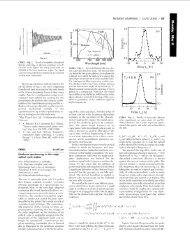
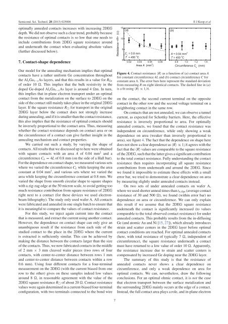
Semicond. Sci. Technol. 28 (2013) 025006optimally annealed <strong>contacts</strong> increases with increasing 2DEGdepth. We did not observe such a clear trend, probably because<strong>the</strong> resistance <strong>of</strong> optimal <strong>contacts</strong> is so low that one needs <strong>to</strong>include contributions from 2DEG square resistance aroundand underneath <strong>the</strong> contact when evaluating absolute values(fur<strong>the</strong>r discussed below).(a)(b)E J Koop et al7. Contact-shape dependenceOur model for <strong>the</strong> <strong>annealing</strong> <strong>mechanism</strong> implies that optimal<strong>contacts</strong> have a ra<strong>the</strong>r uniform Ge concentration throughout<strong>the</strong> Al x Ga 1−x As layers, and that this results in a value for R Ge<strong>of</strong> order 10 . This implies that <strong>the</strong> bulk resistivity in <strong>the</strong>doped Ge-doped Al x Ga 1−x As layer is around 4 m. In turn,this implies that in-plane electron transport under an optimalcontact from <strong>the</strong> metalization on <strong>the</strong> surface <strong>to</strong> 2DEG on <strong>the</strong>side <strong>of</strong> <strong>the</strong> contact still mainly takes place in <strong>the</strong> original 2DEGlayer. If <strong>the</strong> square resistance R □ for transport in <strong>the</strong> original2DEG layer below <strong>the</strong> contact does not strongly increaseduring <strong>annealing</strong>, and if it is smaller than <strong>the</strong> contact resistance,this also implies that <strong>the</strong> resistance <strong>of</strong> optimal <strong>contacts</strong> shouldbe inversely proportional <strong>to</strong> <strong>the</strong> contact area. Thus, measuringwhe<strong>the</strong>r <strong>the</strong> contact resistance depends on contact area or on<strong>the</strong> circumference <strong>of</strong> a contact can give fur<strong>the</strong>r insight in <strong>the</strong><strong>annealing</strong> <strong>mechanism</strong> and contact properties.We carried out such a study, by varying <strong>the</strong> shape <strong>of</strong><strong>contacts</strong>. All results that we discussed up <strong>to</strong> here were obtainedwith square <strong>contacts</strong> with an area A <strong>of</strong> 0.04 mm 2 and acircumference C L = 4L <strong>of</strong> 0.8 mm (on <strong>the</strong> side <strong>of</strong> a Hall bar).For <strong>the</strong> dependence on contact shape, we measured various setswhere we varied <strong>the</strong> circumference C L while keeping <strong>the</strong> areaconstant at 0.04 mm 2 , and various sets where we varied <strong>the</strong>area while keeping <strong>the</strong> circumference constant at 0.8 mm. Wevaried <strong>the</strong> shape from smooth circular shape <strong>to</strong> square shapeswith a zig-zag edge at <strong>the</strong> 50 micron scale, <strong>to</strong> avoid getting <strong>to</strong>omuch resistance contribution from square resistance <strong>of</strong> 2DEGright next <strong>to</strong> a contact (for <strong>the</strong>se devices we used electronbeamlithography). The study only used wafer A. All <strong>contacts</strong>were fabricated and annealed in one single batch <strong>to</strong> ensure thatit is meaningful <strong>to</strong> compare <strong>the</strong> values <strong>of</strong> contact resistance.For this study, we inject again current in<strong>to</strong> <strong>the</strong> contactthat is measured, and extract <strong>the</strong> current using ano<strong>the</strong>r contact.However, <strong>the</strong> dependence on contact shape can only give anunambiguous result if <strong>the</strong> resistance from each side <strong>of</strong> <strong>the</strong>studied contact <strong>to</strong> <strong>the</strong> place in <strong>the</strong> 2DEG where <strong>the</strong> currentis extracted is sufficiently similar. This can be achieved bymaking <strong>the</strong> distance between <strong>the</strong> <strong>contacts</strong> larger than <strong>the</strong> size<strong>of</strong> <strong>the</strong> <strong>contacts</strong>. Thus, we now fabricated <strong>contacts</strong> in <strong>the</strong> middle<strong>of</strong> 2 mm × 3 mm cleaved wafer pieces (<strong>two</strong> rows <strong>of</strong> four<strong>contacts</strong>, with center-<strong>to</strong>-center distance between rows 1 mmand center-<strong>to</strong>-center distance between <strong>contacts</strong> within a row0.6 mm). Using four different <strong>contacts</strong> for a four-terminalmeasurement on <strong>the</strong> 2DEG (with <strong>the</strong> current biased from onerow <strong>to</strong> <strong>the</strong> o<strong>the</strong>r) gives on <strong>the</strong>se samples indeed low valuesaround 8 , in reasonable agreement with <strong>the</strong> value <strong>of</strong> <strong>the</strong>2DEG square resistance R □ <strong>of</strong> about 20 . Contact resistancevalues were again determined in a current-biased four-terminalconfiguration, with <strong>two</strong> terminals connected <strong>to</strong> <strong>the</strong> bond wireFigure 4. Contact resistance 〈R〉 as a function <strong>of</strong> (a) contact area Afor constant circumference 4L and (b) contact circumference C forconstant area A. The error bars here represent <strong>the</strong> standard deviationfrom measuring R on eight identical <strong>contacts</strong>. The dashed line in (a)is a fit using 〈R〉 ∝ 1/A.on <strong>the</strong> contact, <strong>the</strong> second current terminal on <strong>the</strong> oppositecontact in <strong>the</strong> o<strong>the</strong>r row and <strong>the</strong> second voltage terminal on aneighboring contact in <strong>the</strong> same row.<strong>On</strong> <strong>contacts</strong> that are not annealed, we can observe a tunnelcurrent, as expected for Schottky barriers. Here, <strong>the</strong> effectiveresistance is inversely proportional <strong>to</strong> area. For optimallyannealed <strong>contacts</strong>, we found that <strong>the</strong> contact resistance wasindependent on circumference, while only showing a weakdependence on area (weaker than inversely proportional <strong>to</strong>area), see figure 4. The fact that <strong>the</strong> dependence on shape heredoes not show a clear dependence as 〈R〉 ∝ 1/A agrees with <strong>the</strong>fact that <strong>the</strong> 〈R〉 values are comparable <strong>to</strong> <strong>the</strong> square resistance<strong>of</strong> <strong>the</strong> 2DEG, such that <strong>the</strong> latter gives a significant contribution<strong>to</strong> <strong>the</strong> <strong>to</strong>tal contact resistance. Fully understanding <strong>the</strong> contactresistance <strong>the</strong>n requires incorporating all square resistancecontributions from underneath and around <strong>the</strong> 2DEG. Sincewe found it impossible <strong>to</strong> estimate <strong>the</strong>se effects with a smallerror bar, we tried <strong>to</strong> demonstrate a clear dependence on areaby measuring slightly under annealed <strong>contacts</strong> instead.<strong>On</strong> <strong>two</strong> sets <strong>of</strong> under annealed <strong>contacts</strong> on wafer A,where we used shorter anneal times than t A,Opt (average contactresistance <strong>of</strong> 30 and 500 ), we found (within error bar) nodependence on area or circumference. We can only explainthis result if we assume that <strong>the</strong> 2DEG square resistanceunderneath <strong>the</strong> contact is significantly increased (<strong>to</strong> valuescomparable <strong>to</strong> <strong>the</strong> <strong>to</strong>tal observed contact resistance) for underannealed <strong>contacts</strong>. This probably results from <strong>the</strong> in-diffusingGe (and a<strong>to</strong>mic <strong>Au</strong> and <strong>Ni</strong> [15, 27]), which already introducesstrain and scatter centers in <strong>the</strong> 2DEG layer before optimalcontact conditions are reached. For optimal annealed <strong>contacts</strong>(here, with <strong>to</strong>tal resistance <strong>of</strong> typically 7 , independent <strong>of</strong>circumference), <strong>the</strong> square resistance underneath a contactmust have returned <strong>to</strong> a low value <strong>of</strong> order 10 . Apparently,<strong>the</strong> resistance increase due <strong>to</strong> strain and scatter centers iscompensated by increased Ge doping near <strong>the</strong> 2DEG layer.The summary <strong>of</strong> this study is that <strong>the</strong> resistance <strong>of</strong>annealed <strong>contacts</strong> never shows a clear dependence oncircumference, and only a weak dependence on area foroptimal <strong>contacts</strong>. We can, never<strong>the</strong>less, draw <strong>the</strong> followingconclusions. For an optimal <strong>ohmic</strong> contact, it is not <strong>the</strong> casethat electron transport between <strong>the</strong> surface metalization and<strong>the</strong> surrounding 2DEG mainly occurs at <strong>the</strong> edge <strong>of</strong> a contact.Instead, <strong>the</strong> full contact area plays a role, and in-plane electron7