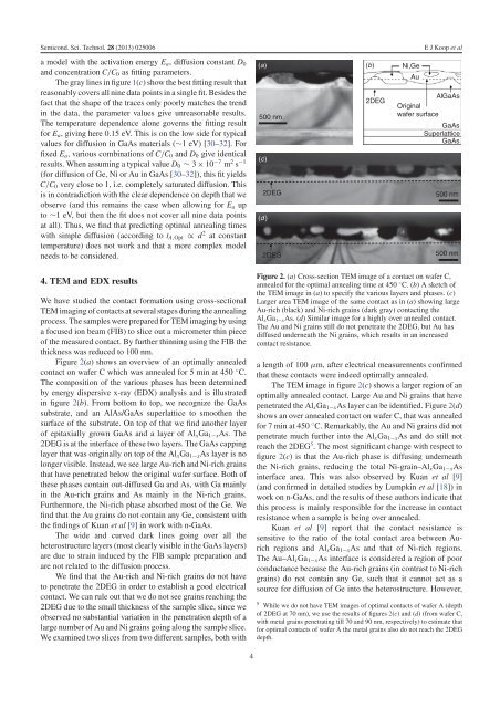
Semicond. Sci. Technol. 28 (2013) 025006E J Koop et ala model with <strong>the</strong> activation energy E a , diffusion constant D 0and concentration C/C 0 as fitting parameters.The gray lines in figure 1(c) show <strong>the</strong> best fitting result thatreasonably covers all nine data points in a single fit. Besides <strong>the</strong>fact that <strong>the</strong> shape <strong>of</strong> <strong>the</strong> traces only poorly matches <strong>the</strong> trendin <strong>the</strong> data, <strong>the</strong> parameter values give unreasonable results.The temperature dependence alone governs <strong>the</strong> fitting resultfor E a , giving here 0.15 eV. This is on <strong>the</strong> low side for typicalvalues for diffusion in GaAs materials (∼1 eV) [30–32]. Forfixed E a , various combinations <strong>of</strong> C/C 0 and D 0 give identicalresults. When assuming a typical value D 0 ∼ 3×10 −7 m 2 s −1(for diffusion <strong>of</strong> Ge, <strong>Ni</strong> or <strong>Au</strong> in GaAs [30–32]), this fit yieldsC/C 0 very close <strong>to</strong> 1, i.e. completely saturated diffusion. Thisis in contradiction with <strong>the</strong> clear dependence on depth that weobserve (and this remains <strong>the</strong> case when allowing for E a up<strong>to</strong> ∼1 eV, but <strong>the</strong>n <strong>the</strong> fit does not cover all nine data pointsat all). Thus, we find that predicting optimal <strong>annealing</strong> timeswith simple diffusion (according <strong>to</strong> t A,Opt ∝ d 2 at constanttemperature) does not work and that a more complex modelneeds <strong>to</strong> be considered.(a)500 nm(c)2DEG(d )2DEG(b)2DEG<strong>Ni</strong>,Ge<strong>Au</strong>AlGaAsOriginalwafer surfaceGaAsSuperlatticeGaAs500 nm500 nm4. TEM and EDX resultsWe have studied <strong>the</strong> contact formation using cross-sectionalTEM imaging <strong>of</strong> <strong>contacts</strong> at several stages during <strong>the</strong> <strong>annealing</strong>process. The samples were prepared for TEM imaging by usinga focused ion beam (FIB) <strong>to</strong> slice out a micrometer thin piece<strong>of</strong> <strong>the</strong> measured contact. By fur<strong>the</strong>r thinning using <strong>the</strong> FIB <strong>the</strong>thickness was reduced <strong>to</strong> 100 nm.Figure 2(a) shows an overview <strong>of</strong> an optimally annealedcontact on wafer C which was annealed for 5 min at 450 ◦ C.The composition <strong>of</strong> <strong>the</strong> various phases has been determinedby energy dispersive x-ray (EDX) analysis and is illustratedin figure 2(b). From bot<strong>to</strong>m <strong>to</strong> <strong>to</strong>p, we recognize <strong>the</strong> GaAssubstrate, and an AlAs/GaAs superlattice <strong>to</strong> smoo<strong>the</strong>n <strong>the</strong>surface <strong>of</strong> <strong>the</strong> substrate. <strong>On</strong> <strong>to</strong>p <strong>of</strong> that we find ano<strong>the</strong>r layer<strong>of</strong> epitaxially grown GaAs and a layer <strong>of</strong> Al x Ga 1−x As. The2DEG is at <strong>the</strong> interface <strong>of</strong> <strong>the</strong>se <strong>two</strong> layers. The GaAs cappinglayer that was originally on <strong>to</strong>p <strong>of</strong> <strong>the</strong> Al x Ga 1−x As layer is nolonger visible. Instead, we see large <strong>Au</strong>-rich and <strong>Ni</strong>-rich grainsthat have penetrated below <strong>the</strong> original wafer surface. Both <strong>of</strong><strong>the</strong>se phases contain out-diffused Ga and As, with Ga mainlyin <strong>the</strong> <strong>Au</strong>-rich grains and As mainly in <strong>the</strong> <strong>Ni</strong>-rich grains.Fur<strong>the</strong>rmore, <strong>the</strong> <strong>Ni</strong>-rich phase absorbed most <strong>of</strong> <strong>the</strong> Ge. Wefind that <strong>the</strong> <strong>Au</strong> grains do not contain any Ge, consistent with<strong>the</strong> findings <strong>of</strong> Kuan et al [9] in work with n-GaAs.The wide and curved dark lines going over all <strong>the</strong>heterostructure layers (most clearly visible in <strong>the</strong> GaAs layers)are due <strong>to</strong> strain induced by <strong>the</strong> FIB sample preparation andare not related <strong>to</strong> <strong>the</strong> diffusion process.We find that <strong>the</strong> <strong>Au</strong>-rich and <strong>Ni</strong>-rich grains do not have<strong>to</strong> penetrate <strong>the</strong> 2DEG in order <strong>to</strong> establish a good electricalcontact. We can rule out that we do not see grains reaching <strong>the</strong>2DEG due <strong>to</strong> <strong>the</strong> small thickness <strong>of</strong> <strong>the</strong> sample slice, since weobserved no substantial variation in <strong>the</strong> penetration depth <strong>of</strong> alarge number <strong>of</strong> <strong>Au</strong> and <strong>Ni</strong> grains going along <strong>the</strong> sample slice.We examined <strong>two</strong> slices from <strong>two</strong> different samples, both withFigure 2. (a) Cross-section TEM image <strong>of</strong> a contact on wafer C,annealed for <strong>the</strong> optimal <strong>annealing</strong> time at 450 ◦ C. (b) A sketch <strong>of</strong><strong>the</strong> TEM image in (a) <strong>to</strong> specify <strong>the</strong> various layers and phases. (c)Larger area TEM image <strong>of</strong> <strong>the</strong> same contact as in (a) showing large<strong>Au</strong>-rich (black) and <strong>Ni</strong>-rich grains (dark gray) contacting <strong>the</strong>Al x Ga 1−x As. (d) Similar image for a highly over annealed contact.The <strong>Au</strong> and <strong>Ni</strong> grains still do not penetrate <strong>the</strong> 2DEG, but <strong>Au</strong> hasdiffused underneath <strong>the</strong> <strong>Ni</strong> grains, which results in an increasedcontact resistance.a length <strong>of</strong> 100 µm, after electrical measurements confirmedthat <strong>the</strong>se <strong>contacts</strong> were indeed optimally annealed.The TEM image in figure 2(c) shows a larger region <strong>of</strong> anoptimally annealed contact. Large <strong>Au</strong> and <strong>Ni</strong> grains that havepenetrated <strong>the</strong> Al x Ga 1−x As layer can be identified. Figure 2(d)shows an over annealed contact on wafer C, that was annealedfor 7 min at 450 ◦ C. Remarkably, <strong>the</strong> <strong>Au</strong> and <strong>Ni</strong> grains did notpenetrate much fur<strong>the</strong>r in<strong>to</strong> <strong>the</strong> Al x Ga 1−x As and do still notreach <strong>the</strong> 2DEG 5 . The most significant change with respect t<strong>of</strong>igure 2(c) is that <strong>the</strong> <strong>Au</strong>-rich phase is diffusing underneath<strong>the</strong> <strong>Ni</strong>-rich grains, reducing <strong>the</strong> <strong>to</strong>tal <strong>Ni</strong>-grain–Al x Ga 1−x Asinterface area. This was also observed by Kuan et al [9](and confirmed in detailed studies by Lumpkin et al [18]) inwork on n-GaAs, and <strong>the</strong> results <strong>of</strong> <strong>the</strong>se authors indicate thatthis process is mainly responsible for <strong>the</strong> increase in contactresistance when a sample is being over annealed.Kuan et al [9] report that <strong>the</strong> contact resistance issensitive <strong>to</strong> <strong>the</strong> ratio <strong>of</strong> <strong>the</strong> <strong>to</strong>tal contact area between <strong>Au</strong>richregions and Al x Ga 1−x As and that <strong>of</strong> <strong>Ni</strong>-rich regions.The <strong>Au</strong>–Al x Ga 1−x As interface is considered a region <strong>of</strong> poorconductance because <strong>the</strong> <strong>Au</strong>-rich grains (in contrast <strong>to</strong> <strong>Ni</strong>-richgrains) do not contain any Ge, such that it cannot act as asource for diffusion <strong>of</strong> Ge in<strong>to</strong> <strong>the</strong> heterostructure. However,5 While we do not have TEM images <strong>of</strong> optimal <strong>contacts</strong> <strong>of</strong> wafer A (depth<strong>of</strong> 2DEG at 70 nm), we use <strong>the</strong> results <strong>of</strong> figures 2(c) and (d) (from wafer C,with metal grains penetrating till 70 and 90 nm, respectively) <strong>to</strong> estimate thatfor optimal <strong>contacts</strong> <strong>of</strong> wafer A <strong>the</strong> metal grains also do not reach <strong>the</strong> 2DEGdepth.4
Semicond. Sci. Technol. 28 (2013) 025006it is <strong>to</strong> our knowledge not yet unders<strong>to</strong>od why <strong>the</strong> diffusion <strong>of</strong><strong>Au</strong> underneath <strong>the</strong> <strong>Ni</strong> grains at later stages <strong>of</strong> <strong>annealing</strong> (whena large amount <strong>of</strong> Ge already diffused out <strong>of</strong> <strong>Ni</strong>) results in astrong increase <strong>of</strong> <strong>the</strong> contact resistance.5. Summary <strong>of</strong> <strong>annealing</strong> <strong>mechanism</strong>In this section, we use <strong>the</strong> results from <strong>the</strong> previous <strong>two</strong>sections, <strong>to</strong>ge<strong>the</strong>r with established results from <strong>the</strong> literature,for giving a qualitative description <strong>of</strong> <strong>the</strong> formation <strong>of</strong> an <strong>ohmic</strong>contact <strong>to</strong> a 2DEG in a GaAs/Al x Ga 1−x As heterostructure. It isremarkably similar <strong>to</strong> <strong>the</strong> <strong>annealing</strong> <strong>mechanism</strong> as describedby Kuan et al [9] for <strong>contacts</strong> <strong>to</strong> n-GaAs. In <strong>the</strong> initial stages<strong>of</strong> <strong>the</strong> <strong>annealing</strong> process (already during <strong>the</strong> heating <strong>of</strong> <strong>the</strong>sample) <strong>Au</strong> and Ge segregate, and most Ge forms a newphase with <strong>the</strong> <strong>Ni</strong>. At <strong>the</strong> same time, <strong>the</strong>se Ge-rich <strong>Ni</strong> grainsmove <strong>to</strong> <strong>the</strong> wafer surface due <strong>to</strong> a wetting effect [16], whichresults in <strong>the</strong> situation that <strong>the</strong> wafer surface is covered withneighboring <strong>Au</strong> and <strong>Ni</strong> x Ge 6 grains. There is evidence thatfor thin metalization layers (∼100 nm) this process alreadyoccurs well below <strong>the</strong> bulk melting temperature (363 ◦ C) <strong>of</strong><strong>the</strong> eutectic <strong><strong>Au</strong>Ge</strong> phase [16].Next, at higher temperatures, both <strong>the</strong> <strong>Au</strong>-rich and<strong>Ni</strong>-rich grains penetrate in<strong>to</strong> <strong>the</strong> heterostructure by solidphase inter-diffusion, compensated by a back flow <strong>of</strong> Asand Ga. Our EDX results confirm that Ga mainly flows in<strong>to</strong><strong>Au</strong>, and As mainly in<strong>to</strong> <strong>Ni</strong>-rich grains. This concerns <strong>the</strong>formation <strong>of</strong> new material phases. In several earlier studies[9, 19, 12, 14, 16–18] <strong>the</strong>se phases have been identified as<strong>Au</strong>Ga alloys and phases close <strong>to</strong> <strong>Ni</strong> 2 GeAs. These phasespenetrate only tens <strong>of</strong> nm below <strong>the</strong> original wafer surfacefor typical <strong>annealing</strong> conditions [9, 14].At <strong>the</strong> same time, <strong>the</strong>re is diffusion <strong>of</strong> a<strong>to</strong>mic Ge, <strong>Ni</strong> and<strong>Au</strong> (at similar concentrations) in<strong>to</strong> <strong>the</strong> heterostructure, whichpenetrates deeper [8, 19, 20, 15, 27]. In particular, Ge diffusesout <strong>of</strong> <strong>the</strong> <strong>Ni</strong>-rich grains in<strong>to</strong> <strong>the</strong> Al x Ga 1−x As layers, and agood <strong>ohmic</strong> contact is formed when <strong>the</strong> Al x Ga 1−x As layersare sufficiently doped with Ge all <strong>the</strong> way up <strong>to</strong> <strong>the</strong> 2DEG.While this is progressing, <strong>the</strong> <strong>Au</strong>-rich grains start <strong>to</strong> expandunderneath <strong>the</strong> <strong>Ni</strong>-rich grains [9, 18], which have <strong>the</strong> lowestcontact resistance with <strong>the</strong> doped Al x Ga 1−x As layer since <strong>the</strong>ywere <strong>the</strong> dominant supplier <strong>of</strong> Ge. The expansion <strong>of</strong> <strong>the</strong> <strong>Au</strong>Gagrains is possibly due <strong>to</strong> <strong>the</strong> relatively low activation energyfor out diffusion <strong>of</strong> Ga in<strong>to</strong> <strong>Au</strong> [32] (while <strong>the</strong> Al–As bindingenergy is relatively high [19]). This latter process increases <strong>the</strong>interface resistance between <strong>the</strong> metalization on <strong>the</strong> surfaceand <strong>the</strong> doped Al x Ga 1−x As layer. Thus, <strong>the</strong> formation <strong>of</strong> anoptimal contact is a competition between <strong>the</strong>se <strong>two</strong> processes.The in-diffusion <strong>of</strong> Ge lowers <strong>the</strong> contact resistance for<strong>two</strong> reasons. (1) The full Al x Ga 1−x As region between <strong>the</strong>surface and <strong>the</strong> 2DEG becomes a highly doped region with areasonably low bulk resistivity. (2) The Ge doping in this regionmakes <strong>the</strong> Schottky barrier between <strong>the</strong> doped semiconduc<strong>to</strong>rand <strong>the</strong> surface metalization very thin (<strong>the</strong> barrier height is6 Early in <strong>the</strong> <strong>annealing</strong> process, <strong>the</strong> grains mainly containing <strong>Ni</strong> and Ge havebeen identified as <strong>Ni</strong>Ge, <strong>Ni</strong> 2 Ge and <strong>Ni</strong> 3 Ge phases [9, 12].E J Koop et alprobably not changing significantly 7 ), up <strong>to</strong> <strong>the</strong> point where itsseries contribution <strong>to</strong> <strong>the</strong> contact resistance is small. The <strong>to</strong>talcontact resistance is <strong>the</strong>n dominated by doped Al x Ga 1−x Asregion, giving linear transport characteristics (a similar effec<strong>to</strong>ccurs for <strong>contacts</strong> <strong>to</strong> n-GaAs due <strong>to</strong> spreading resistancebelow <strong>the</strong> contact [6]).As said, it is not yet well established which processes areresponsible for <strong>the</strong> resistance increase upon over <strong>annealing</strong>.The fact that over <strong>annealing</strong> with 2DEG samples and n-GaAssamples [9] occurs qualitatively in a very similar manner (andalso at similar <strong>annealing</strong> times and temperatures) is a firstindication that it is due <strong>to</strong> a process near <strong>the</strong> interface withmetal-rich phases on <strong>the</strong> surface, ra<strong>the</strong>r than a process at <strong>the</strong>depth <strong>of</strong> <strong>the</strong> 2DEG or <strong>the</strong> edge <strong>of</strong> a contact. Fur<strong>the</strong>rmore,our results now show that <strong>the</strong> resistance increase for 2DEGsamples is also correlated with <strong>the</strong> expanding <strong>Au</strong>Ga grainsbelow <strong>the</strong> <strong>Ni</strong>-rich grains. Various authors have suggested that<strong>the</strong> increasing contact resistance that is associated with over<strong>annealing</strong> may be due <strong>to</strong> a large number <strong>of</strong> vacancies justbelow <strong>the</strong> metal-rich phases near <strong>the</strong> surface [19, 14, 24](but o<strong>the</strong>rs suggested it was due <strong>to</strong> excessive in-diffusion <strong>of</strong><strong>Ni</strong> [5, 14]). These mainly result from out-diffusion <strong>of</strong> Gain<strong>to</strong> <strong>the</strong> <strong>Au</strong>-rich grains (which indeed results in a very stable<strong>Au</strong>Ga phase near <strong>the</strong> original wafer surface [5, 16, 17]). Thesevacancies occur in particular when <strong>the</strong>re is no (longer) Gediffusion in<strong>to</strong> <strong>the</strong>se vacancies. <strong>On</strong>e should note, however,that with n-GaAs an increasing contact resistance was alsoobserved without an expansion <strong>of</strong> <strong>the</strong> <strong>Au</strong>Ga grains below <strong>the</strong><strong>Ni</strong>-rich grains [14], but this does not rule out that an increasingnumber <strong>of</strong> vacancies is responsible for over <strong>annealing</strong>.Finally, we remark that both <strong>the</strong> <strong>Ni</strong>-rich and <strong>Au</strong>-rich grainsare probably important for rapid <strong>annealing</strong> at relatively lowtemperatures. The <strong>Ni</strong>-rich grains act as <strong>the</strong> supplier <strong>of</strong> Ge. Thepresence <strong>of</strong> <strong>Au</strong> grains may be important since it rapidly resultsin a large number <strong>of</strong> Ga vacancies. This probably enhances<strong>the</strong> in-diffusion <strong>of</strong> Ge. It was for example also observed that<strong>the</strong> creation <strong>of</strong> such vacancies near <strong>the</strong> surface, enhances <strong>the</strong>diffusion <strong>of</strong> Si dopants from <strong>the</strong> doping layer (much deeperin<strong>to</strong> <strong>the</strong> material) in<strong>to</strong> neighboring layers [15].6. Diffusion modelWe use <strong>the</strong> above description <strong>to</strong> construct a model that predicts<strong>the</strong> optimal <strong>annealing</strong> time for a given <strong>annealing</strong> temperatureand 2DEG depth d. The contact resistance is <strong>the</strong>n <strong>the</strong> seriesresistance <strong>of</strong> <strong>the</strong> Ge-doped Al x Ga 1−x As region (R Ge ) and <strong>the</strong>interface resistance between <strong>the</strong> surface metalization and thisGe-doped Al x Ga 1−x As layer (R if ). For both, we consider <strong>the</strong>average over <strong>the</strong> full contact area. We will first assume ananneal temperature T that is constant in time. We model <strong>the</strong>resistance <strong>of</strong> <strong>the</strong> Ge-doped Al x Ga 1−x As region using <strong>the</strong> resultfrom work on n-GaAs that <strong>the</strong> contact resistance is inversely7 It is believed that <strong>the</strong> height <strong>of</strong> <strong>the</strong> Schottky barrier is under all relevantconditions pinned at about 0.8 eV [11]. A lowering <strong>of</strong> <strong>the</strong> Schottky barrierwith <strong>Au</strong>, <strong>Ni</strong> and Ge layers on <strong>the</strong> wafer surface was only observed for veryspecific interfaces [13], and does probably not occur during actual <strong>annealing</strong><strong>of</strong> <strong><strong>Au</strong>Ge</strong>/<strong>Ni</strong>/<strong>Au</strong> <strong>contacts</strong> [12].5