6 Inch 0.1μm GaAs pHEMT Technology for E/V Band ... - CS Mantech
6 Inch 0.1μm GaAs pHEMT Technology for E/V Band ... - CS Mantech
6 Inch 0.1μm GaAs pHEMT Technology for E/V Band ... - CS Mantech

Create successful ePaper yourself
Turn your PDF publications into a flip-book with our unique Google optimized e-Paper software.
6 <strong>Inch</strong> 0.1µm <strong>GaAs</strong> <strong>pHEMT</strong> <strong>Technology</strong> <strong>for</strong> E/V <strong>Band</strong> Application<br />
Hsi-Tsung Lin, Chao-Hong Chen, Shih-Chun Lee, I-Te Cho,<br />
Wen-Kai Wang, and Shinichiro Takatani<br />
WIN Semiconductors Corp. No. 69 <strong>Technology</strong> 7 th Rd, Hwaya <strong>Technology</strong> Park,<br />
Kuei Shan Hsiang, Tao Yuan Shien, Taiwan (333)<br />
Phone: +886-3-3975999 ext. 1735, e-mail: jameslin@winfoundry.com<br />
Keywords: 0.1µm, <strong>GaAs</strong>, <strong>pHEMT</strong>, E band, V band.<br />
Abstract<br />
WIN Semiconductors Corp. has developed a new<br />
<strong>GaAs</strong> <strong>pHEMT</strong> technology with 0.1µm gate length by<br />
using Electron-Beam Lithography and be named as PP10<br />
with the option of 2 mil and 4 mil substrate thickness.<br />
The dc behavior of PP10 illustrates the pinch off<br />
voltage of -0.95 V with excellent Idmax of 760mA when<br />
gate voltage of 0.5V, which achieve the maximum<br />
Transconductance as high as 725mS/mm consequently.<br />
The 130GHz of ft with breakdown voltage of 9V exhibits<br />
the great high frequency and power per<strong>for</strong>mance on this<br />
technology.<br />
According to the extraction of MSG (Maximum Stable<br />
Gain ) from 110 GHz S-parameter measurement, the 8-9<br />
dB gain per<strong>for</strong>mance from 70~90 GHz is detected.<br />
Additionally, the extremely high power density and the<br />
superior per<strong>for</strong>mance of noise figure exhibits the<br />
potential of integrating E/V band’s Tx/Rx core circuit on<br />
one chip by using the PP10.<br />
INTRODUCTION<br />
The MMICs with high per<strong>for</strong>mance - power density and<br />
noise figure - at high frequency will be the key components<br />
in next generation wireless infrastructure, and the<br />
semiconductor devices will almost dominate the overall<br />
per<strong>for</strong>mance. WIN Semiconductors Corp. has developed a<br />
superior per<strong>for</strong>mance 0.1µm <strong>GaAs</strong> <strong>pHEMT</strong> technology,<br />
PP10. With 130GHz F t and 180GHz F max aims V/E band PtP<br />
radios that provide low cost, easy maintenance, and high<br />
data rate of in<strong>for</strong>mation transference. This technology is<br />
produced in 6 inch wafers, high volume of products with<br />
high per<strong>for</strong>mance, will be used in the backhaul of 3G/4G<br />
mobile base station and the radar <strong>for</strong> airport surveillance.<br />
DEVICE STRUCTURES & PROCESS<br />
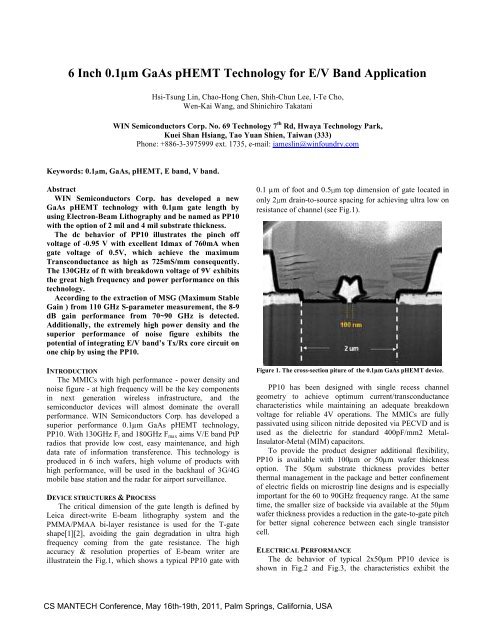
The critical dimension of the gate length is defined by<br />
Leica direct-write E-beam lithography system and the<br />
PMMA/PMAA bi-layer resistance is used <strong>for</strong> the T-gate<br />
shape[1][2], avoiding the gain degradation in ultra high<br />
frequency coming from the gate resistance. The high<br />
accuracy & resolution properties of E-beam writer are<br />
illustratein the Fig.1, which shows a typical PP10 gate with<br />
0.1 µm of foot and 0.5µm top dimension of gate located in<br />
only 2µm drain-to-source spacing <strong>for</strong> achieving ultra low on<br />
resistance of channel (see Fig.1).<br />
Figure 1. The cross-section piture of the 0.1µm <strong>GaAs</strong> <strong>pHEMT</strong> device.<br />
PP10 has been designed with single recess channel<br />
geometry to achieve optimum current/transconductance<br />
characteristics while maintaining an adequate breakdown<br />
voltage <strong>for</strong> reliable 4V operations. The MMICs are fully<br />
passivated using silicon nitride deposited via PECVD and is<br />
used as the dielectric <strong>for</strong> standard 400pF/mm2 Metal-<br />
Insulator-Metal (MIM) capacitors.<br />
To provide the product designer additional flexibility,<br />
PP10 is available with 100µm or 50µm wafer thickness<br />
option. The 50µm substrate thickness provides better<br />
thermal management in the package and better confinement<br />
of electric fields on microstrip line designs and is especially<br />
important <strong>for</strong> the 60 to 90GHz frequency range. At the same<br />
time, the smaller size of backside via available at the 50µm<br />
wafer thickness provides a reduction in the gate-to-gate pitch<br />
<strong>for</strong> better signal coherence between each single transistor<br />
cell.<br />
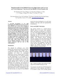
ELECTRICAL PERFORMANCE<br />
The dc behavior of typical 2x50µm PP10 device is<br />
shown in Fig.2 and Fig.3, the characteristics exhibit the<br />
9<br />
b<br />
<strong>CS</strong> MANTECH Conference, May 16th-19th, 2011, Palm Springs, Cali<strong>for</strong>nia, USA<br />
189
pinch off voltage of -0.95V with excellent Idmax of 760<br />
mA/mm when gate voltage of 0.5V, which achieve the<br />
maximum transconductance as high as 750mS/mm<br />
consequently. The knee voltage below a drain voltage of 1V<br />
and gate-to-drain breakdown voltage of 9V result in the<br />
superior large voltage swing area <strong>for</strong> the RF signal, and<br />
when combined with the high current density, could deliver<br />
very high power density.<br />
Figure 4. The maximum gain per<strong>for</strong>mance is measured by 110GHz S-<br />
parameters system. The MSG of both 2x25µm and 2x50µm transistors<br />
could be maintained about 8dB at 90GHz.<br />
Figure 2. The transcoductance curve of PP10. A high current and<br />
trasconductance behavior are observed.<br />
.<br />
Figure 5. 850mW/mm saturated power density could be reached under<br />
29GHz load pull system, the device is operated at drain bias of 4V.<br />
Figure 3. The IV curve of PP10. We can see the knee voltage below a<br />
drain voltage of 1V and superior large voltage swing area <strong>for</strong> the RF<br />
signal.<br />
Fig.6 illustrates F min and associated gain from an<br />
8x25µm PP10 transistor taken at a bias of V ds =2V and<br />
50mA/mm. The excellent noise per<strong>for</strong>mance with a<br />
minimum noise figure of 0.8 dB and associated gain over 9<br />
dB at 40 GHz is achieved.<br />
S-parameter measurements taken at V ds = 2V and<br />
extraction of Maximum Stable Gain (MSG) to 110GHz is<br />
shown in Fig.4 <strong>for</strong> both 2x25µm and 2x50µm transistors.<br />
These data show the PP10 devices provide 8 to 9 dB gain<br />
from 70 to 90 GHz.<br />
On the other hand, the extremely high power density of<br />
850mW/mm at 29 GHz on the device of 2x50µm is detected<br />
under the drain bias of 4V with the gain and maximum<br />
power added efficiency (PAE) of 12dB and 50%,<br />
respectively in Fig.5.<br />
Figure 6. The 26-40GHz noise per<strong>for</strong>mance of PP10 that taken at<br />
V ds=2V and 50mA/mm.<br />
190 <strong>CS</strong> MANTECH Conference, May 16th-19th, 2011, Palm Springs, Cali<strong>for</strong>nia, USA
THE GATE YIELD & UNIFORMITY<br />
Yield of the process is evaluated using FETs with 25<br />
gate fingers and 75um unit width on 150 mm wafers. Yield<br />
data is shown in Fig.7. The uni<strong>for</strong>mity of the fundamental<br />
transistor characteristics, shown in Fig. 8, is measured using<br />
two-gate-finger devices.<br />
ACRONYMS<br />
MMIC: Monolithic microwave integrated circuit.<br />
<strong>pHEMT</strong>: High electron mobility transistor .<br />
MIM: Metal-Insulator-Metal capacitors.<br />
MSG: Maximum Stable Gain.<br />
PAE: Maximum power added efficiency.<br />
Pinch-off current (mA/mm)<br />
0.003<br />
Breakdown voltage (V)<br />
9.5<br />
0.003 0.003 0.003 0.003 0.003<br />
9.5 9.5 9.6 9.6 9.7<br />
0.004 0.003 0.003 0.003 0.003 0.003<br />
9.4 9.7 9.6 9.4 9.5 9.7<br />
0.007 0.004 0.003 0.003 0.004 0.004 0.004<br />
9.3 9.6 9.6 9.5 9.4 9.3 9.4<br />
0.004 0.004 0.003 0.004 0.004<br />
9.3 9.6 9.6 9.4 9.4<br />
0.004<br />
9.6<br />
Figure 7. The gate yield is determined by gate leakage, pinch-off, and<br />
breakdown per<strong>for</strong>mance of the 25×75µm device.<br />
Figure 8. The wafer maps of the key parameters of 2×75µm device<br />
show high uni<strong>for</strong>mity.<br />
CONCLUSIONS<br />
The short gate length and the specific design on Epi and<br />
process of PP10 result in competitive power and noise<br />
per<strong>for</strong>mance simultaneously. It allows the product designer<br />
to realize a highly integrated multifunctional device with<br />
high power amplifier, medium power amplifier and low<br />
noise amplifier on one chip <strong>for</strong> the E-band to V-band Tx/Rx<br />
core circuit. With the cost effective 6 inch process capability,<br />
the 0.1µm <strong>GaAs</strong> <strong>pHEMT</strong> technology could be the right<br />
technology <strong>for</strong> the development of new generation E/V band<br />
radio application.<br />
ACKNOWLEDGEMENTS<br />
We would like to appreciate <strong>for</strong> the support on the<br />
110GHz S-parameter measurement from the Dr. Robin<br />
Sloan of Manchester University UK.<br />
9<br />
b<br />
REFERENCES<br />
[1] M. Chertouk, D. W. Tu, et al, “Manufacturable 0.15 um<br />
PHEMT Process <strong>for</strong> High Volume and Low Cost on 6”<br />
<strong>GaAs</strong> Substrates : The First 0.15 µm PHEMT 6”<strong>GaAs</strong><br />
Foundry Fab”, <strong>GaAs</strong> <strong>Mantech</strong> Conf. April 2002.<br />
[2] H.C. Chou, M.C. Liao, et al, “Design of Experiments to<br />
Achieve High Yield Manufacturing at 6-inch Foundry”,<br />
<strong>GaAs</strong> <strong>Mantech</strong> Conf. April 2002.<br />
<strong>CS</strong> MANTECH Conference, May 16th-19th, 2011, Palm Springs, Cali<strong>for</strong>nia, USA<br />
191