Analysis and design of a 200W LDMOS based doherty amplifier for ...
Analysis and design of a 200W LDMOS based doherty amplifier for ...
Analysis and design of a 200W LDMOS based doherty amplifier for ...

You also want an ePaper? Increase the reach of your titles
YUMPU automatically turns print PDFs into web optimized ePapers that Google loves.
WE5A-3<br />
<strong>Analysis</strong> <strong>and</strong> Design <strong>of</strong> a <strong>200W</strong> <strong>LDMOS</strong> Based<br />
Doherty Amplifier <strong>for</strong> 3G Base Stations<br />
John R. Gajadharsing, Ol<strong>of</strong> Bosma*, <strong>and</strong> Pim van Westen*<br />
Philips Semiconductors, BU Mobile Communications, Nijmegen, The Netherl<strong>and</strong>s<br />
*MAP, Meerlaan 21, 1671 ED, Medemblik, The Netherl<strong>and</strong>s<br />
Abstract - In tbis paper the analy& <strong>and</strong> <strong>design</strong> <strong>of</strong> a<br />
2OOW classical Doherty <strong>amplifier</strong> is described using dlscrete<br />
<strong>LDMOS</strong> devices. The peak (class-C) <strong>and</strong> main (class-AB)<br />
<strong>amplifier</strong>s are desigbed with two stages to obtain flat AM-<br />
AM <strong>and</strong> AM-PM charPCteristics <strong>for</strong> the Doherty <strong>amplifier</strong>.<br />
An asymmetrical planar coupler structure is uWed as an<br />
input splitter <strong>and</strong> microship <strong>based</strong> elements are used <strong>for</strong><br />
phase matching <strong>and</strong> power combloing at the output. Thh<br />
Doherty PA has a measured PldB <strong>of</strong> 53dBm <strong>and</strong> exhibits an<br />
efiiciency <strong>of</strong> 34% at 6dB back<strong>of</strong>f (47") <strong>for</strong> two-carrier<br />
WCDMA. The ACPR <strong>and</strong> IM3 obtained at 47dBm are 37dBc<br />
<strong>and</strong> 33dBc respectively. The gain at 6dB back<strong>of</strong>f is ZZdB over<br />
the frequency range 2.11-2.17GHz Design considerations <strong>for</strong><br />
a Doherty ampMer <strong>based</strong> on discrete <strong>LDMOS</strong> devices are<br />
addressed.<br />
Index terms - Doherty, <strong>LDMOS</strong>, AM-AM, AM-PM,<br />
WCDMA, power amplifiem<br />
I. INTRODUCTION<br />
In contemporary base stations <strong>amplifier</strong> <strong>design</strong>s <strong>for</strong><br />
WCDMA, one <strong>of</strong> the main concerns is the power<br />
consumption. Due to the linearity requirements the<br />
operating point <strong>of</strong> these <strong>amplifier</strong>s are constrained to the<br />
backdff region where it is not most efficient. Although<br />
we can still expect to see @proved back<strong>of</strong>f efficiency<br />
through advancement in device technology it is<br />
theoretically limited. The Doherty <strong>amplifier</strong> is a technique<br />
<strong>for</strong> improving the efficiency <strong>of</strong> backed-<strong>of</strong>f <strong>amplifier</strong>s<br />
beyond the limits <strong>of</strong> conventional <strong>amplifier</strong>s.<br />
In this paper we will discuss a <strong>200W</strong> <strong>amplifier</strong> <strong>design</strong><br />
<strong>for</strong> WCDMA that has a significantly improved efficiency<br />
in the back<strong>of</strong>f region using discrete <strong>LDMOS</strong> devices.<br />
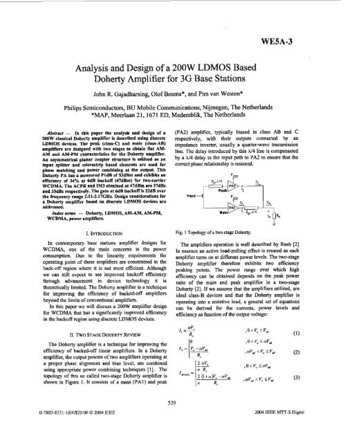
(PAZ) <strong>amplifier</strong>, typically biased in class AB <strong>and</strong> C<br />
respectively, with their outputs connected by an<br />
impedance inverter, usually a quarter-wave transmission<br />
line. The delay introduced by this N4 line is compensated<br />
by a N4 delay in the input path to PA2 to ensure that the<br />
correct phase relationship is restored.<br />
Input 4<br />
Peak<br />
"DD<br />
Fig. 1 Topology <strong>of</strong> a two stage Dohem.<br />
The <strong>amplifier</strong>s operation is well described hy Raab [2]<br />
In essence an active load-pulling effect is created as each<br />
<strong>amplifier</strong> tums on at different power levels. The two-stage<br />
Doherty <strong>amplifier</strong> there<strong>for</strong>e exhibits two efficiency<br />
peaking points. The power range over which high<br />
efficiency can be obtained depends on the peak power<br />
ratio <strong>of</strong> the main <strong>and</strong> peak <strong>amplifier</strong> in a two-stage<br />
Doherty [2]. If we assume that the <strong>amplifier</strong>s utilized, are<br />
ideal class-B devices <strong>and</strong> that the Doherty <strong>amplifier</strong> is<br />
operating into a resistive load, a general set <strong>of</strong> equations<br />
can be derived <strong>for</strong> the currents, power levels <strong>and</strong><br />
efficiency as function <strong>of</strong> the output voltage:<br />
11. Two STAGE DOHERR &VIEW<br />
The Doherty <strong>amplifier</strong> is a technique <strong>for</strong> improving the<br />
efficiency <strong>of</strong> backed-<strong>of</strong>f linear <strong>amplifier</strong>s. In a Doherty<br />
<strong>amplifier</strong>, the output powers <strong>of</strong> two <strong>amplifier</strong>s operating at<br />
a proper phase alignment <strong>and</strong> bias level, are combined<br />
using appropriate power combining techniques [l]. The<br />
topology <strong>of</strong> this so called two-stage Doherty <strong>amplifier</strong> is<br />
shown in Figure 1. It consists <strong>of</strong> a main (PAl) <strong>and</strong> peak<br />
0-7803-8331-1/04/$20.00 Q 2004 IEEE<br />
529<br />
2004 IEEE MTT-S Digest
The individual power levels as indicated in Fig.] are<br />
plotted (4)
e lost when the Doherty <strong>amplifier</strong> is operating below its<br />
transition point. It is there<strong>for</strong>e necessary to add a driver<br />
stage to maximize efficiency. A driver is also added to the<br />
main <strong>amplifier</strong> to accommodate shaping <strong>of</strong> the transfer<br />
characteristics, which is critical in a Doherty <strong>amplifier</strong>.<br />
The splitter asymmetry (A) is set by the gain difference:<br />
A=G,-G, (9)<br />
The gain <strong>of</strong> the total Doherty <strong>amplifier</strong>, at full power, can<br />
then be determined from:<br />
Gm, - 3 +GI - IOlog(l+ (10)<br />
In order to maintain a constant gain over power <strong>for</strong> the<br />
total Doherty <strong>amplifier</strong>, the gain characteristics (AWAM)<br />
<strong>of</strong> the peak <strong>amplifier</strong> should be matched to that <strong>of</strong> the<br />
main <strong>amplifier</strong>, <strong>and</strong>,can be determined from:<br />
G, = 101og(lO"'lo(l+ IOd~~o)-lOG1po)- A (1 1)<br />
The <strong>amplifier</strong>s are <strong>design</strong>ed using internally matched<br />
Philips <strong>LDMOS</strong> transistors. In order to get maximum<br />
efficiency improvement in a Doherty <strong>amplifier</strong> the<br />
transistors need to have specific properties. The transistor<br />
<strong>for</strong> the peak <strong>amplifier</strong> should he <strong>design</strong>ed to have a high<br />
<strong>of</strong>f-state output impedance <strong>and</strong> exhibit low reverse RF<br />
drive. For the main <strong>amplifier</strong> the transistor should he able<br />
to provide maximum per<strong>for</strong>mance under the load pulling<br />
conditions.<br />
The implementation <strong>of</strong> the two-stage class-AB main<br />
<strong>amplifier</strong>, using two BLF2022-40 (5OWpeak) in the final<br />
stage <strong>and</strong> one BLF2043(10W) in the driver stage, is<br />
shown in Fig. 5. The final stage devices are paralleled<br />
without using a quadrature combiner, since both<br />
transistors must experience in-phase load-pulling <strong>for</strong><br />
Doherty operation. The interstage matching is <strong>design</strong>ed to<br />
meet the b<strong>and</strong>width requirement <strong>of</strong> 60MHz <strong>and</strong> to obtain<br />
approximately 3dB compression required <strong>for</strong> Doherty<br />
operation.<br />
Fig. 5. Class-AB main <strong>amplifier</strong> implementation.<br />
The resulting M AM <strong>and</strong> AMPM characteristics <strong>for</strong> a<br />
50n load are shown in Fig. 6 with a peak power capability<br />
<strong>of</strong> 1oow.<br />
Poldhl<br />
Fig. 6. AM-AM <strong>and</strong> AM-PM characteristics <strong>of</strong> the class-AB<br />
main <strong>amplifier</strong> <strong>for</strong> a 5011 load:<br />
The implementation <strong>of</strong> the two-stage class-C peak<br />
<strong>amplifier</strong> is shown in Fig. 7. It utilizes two BLF2022-40 in<br />
the final stage <strong>and</strong> one similar device in the driver stage.<br />
The interstage circuit not only provides impedance<br />
matching but also the correct phase matching between the<br />
driver output <strong>and</strong> final stage input in order to obtain a<br />
predistortion effect that aligns the M AM <strong>and</strong> AM/PM<br />
characteristics <strong>of</strong> the peak <strong>amplifier</strong> with main <strong>amplifier</strong>.<br />
The resulting M AM <strong>and</strong> AWM characteristics <strong>for</strong> a<br />
50n load are shown in Fig. 8 with a peak power capability<br />
<strong>of</strong> 1oow.<br />
Fig. 7. Class-C peak <strong>amplifier</strong> implementation.<br />
X I I I I I I I -,&a<br />
0 . . . . .. . .. .. . . -155<br />
a11 21 zs a U 24 xi Y U) e " 48 4a a U<br />
hldbl<br />
Fig. 8. AM-AM <strong>and</strong> AM-PM characteristics <strong>of</strong> the class-C peak<br />
<strong>amplifier</strong> <strong>for</strong> a 5On load.<br />
Fig. 9 shows the circuit diagram <strong>of</strong> the total Doberty<br />
implementation. The transmission lines TL3 <strong>and</strong> TL4 are<br />
used to maximize overall efficiency. TL3 provides the<br />
phase matching to rotate the <strong>of</strong>f-state impedance <strong>of</strong> the<br />
peak <strong>amplifier</strong> to a high impedance level at the combining<br />
point between TL5 <strong>and</strong> TL6. TL4 provides the phase<br />
matching to ensure that a resistive load <strong>of</strong> twice the<br />
nominal value is presented at the die level <strong>of</strong> the main PA<br />
transistors. The input utilizes an asymmetrical (5dB)<br />
branch line coupler as a splitter. TLl <strong>and</strong> TJ2 are added to<br />
53 1
~<br />
~~~ .,<br />
~~ .<br />
ensure that the output arrive in phase at the combining<br />
point.<br />
IM3 obtained at 47dBm are 37dBc <strong>and</strong> 33dBc<br />
respectively. The gain at 6dB back-<strong>of</strong>f is 22dB over the<br />
frequency range 2.11-2.17GHz.<br />
x1<br />
21:<br />
. ~<br />
. ~~,~<br />
.............<br />
Fig. 9. Schematic <strong>of</strong> the Dohaty implementation.<br />
SCC<br />
c<br />
The AMIAM <strong>and</strong> AM/F’M characteristics <strong>of</strong> the total<br />
Doherty system are shown in Fig. 10. The contribution <strong>of</strong><br />
the peak <strong>amplifier</strong> becomes significant above 48dBm.<br />
4 10<br />
>3 15<br />
n r)<br />
P : ::<br />
137<br />
I8 %i<br />
-10<br />
-3s<br />
a<br />
S D Y S X I ~ 4 U I I B B Y<br />
”1-1<br />
Fig. IO. AM-AM <strong>and</strong> AM-PM characteristics <strong>of</strong> the total<br />
Doherty <strong>amplifier</strong>.<br />
,I<br />
I<br />
Y a I<br />
U,., 47 50 53<br />
Fig. 11. CW gain <strong>and</strong> efficiency <strong>of</strong> the total Doherty <strong>amplifier</strong> at<br />
t 2.14GHz.<br />
:li.<br />
g15<br />
5 ( 0<br />
1~ ~-~ .<br />
. ~<br />
i\;<br />
I_ ma 1Dx) m 2130 ma 2

![P-CAD EDA - [Sheet1]](https://img.yumpu.com/49470492/1/190x115/p-cad-eda-sheet1.jpg?quality=85)