Wideband Gain Block Amplifier Design Techniques
Wideband Gain Block Amplifier Design Techniques
Wideband Gain Block Amplifier Design Techniques

Create successful ePaper yourself
Turn your PDF publications into a flip-book with our unique Google optimized e-Paper software.
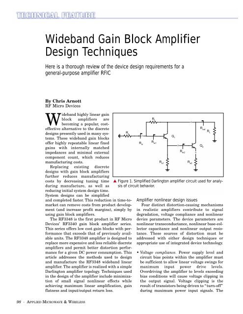
<strong>Wideband</strong> <strong>Gain</strong> <strong>Block</strong> <strong>Amplifier</strong><strong>Design</strong> <strong>Techniques</strong>Here is a thorough review of the device design requirements for ageneral-purpose amplifier RFICBy Chris ArnottRF Micro Devices<strong>Wideband</strong> highly linear gainblock amplifiers arebecoming a popular, costeffectivealternative to the discretedesigns presently used in many systems.These wideband gain blocksoffer highly repeatable linear fixedgains with internally matchedimpedances and minimal externalcomponent count, which reducesmanufacturing costs.Replacing existing discretedesigns with gain block amplifiersfurther reduces manufacturingcosts by decreasing tuning timeduring manufacture, as well asreducing initial system design time.System designs can be simplifiedand completed faster. This reduction in time-tomarketcan remove costs from product development(and increase profit margins), simply byusing gain block amplifiers.The RF3348 is the first product in RF MicroDevices’ RF3340 gain block amplifier series.This series offers low cost gain blocks with performancethat exceeds that of previously availableunits. The RF3348 amplifier is designed toreplace more expensive and less reliable discreteamplifiers and permit better distortion performancefor a given DC power consumption. Thisarticle addresses the methods used to designand manufacture the RF3348 wideband linearamplifier. The amplifier is realized with a simpleDarlington amplifier topology. <strong>Techniques</strong> usedin the design of the amplifier include minimizationof small signal nonlinear effects whileachieving maximum linear amplification, gainflatness and input/output return loss.R s1R inR f4R outR LR e1R e2R in1Q 12Q 2▲ Figure 1. Simplified Darlington amplifier circuit used for analysisof circuit behavior.R in2<strong>Amplifier</strong> nonlinear design issuesFour distinct distortion-causing mechanismsin realistic amplifiers contribute to signaldegradation, voltage compliance and nonlineardevice parameters. The device parameters arenonlinear transconductance, nonlinear base-collectorcapacitance and nonlinear output resistance.These sources of distortion must beaddressed with either design techniques orappropriate use of integrated device technology.• Voltage compliance. Power supply level andcircuit bias points within the amplifier mustbe sufficient to allow linear voltage swings formaximum input power drive levels.Overdriving the amplifier to levels exceedingbias conditions will cause voltage clipping inthe output signal. Voltage clipping is theresult of transistors being driven to “turn-off”during maximum power input signals. The598 · APPLIED MICROWAVE & WIRELESS
power supply level must be selected to provide adequatebias and voltage headroom for maximum outputpower levels. Typically, an RF choke provides amplifierbias by directly connecting the output to the DClevel of the power supply. This bias configurationallows the output signal to swing around the averageDC level of the power supply. Large negative outputswings act as a decreasing power supply and tend toturn the amplifier off, which causes voltage clipping.• Nonlinear transconductance. The exponential I-Vcharacteristics of BJT devices inherently exhibit nonlinearoperation when operated in an open loop state.Using emitter degeneration and shunt feedback withadequate bias current can permit the amplifier toobtain very good linear operation.• Nonlinear amplifier input/output impedance.Nonlinear variations in amplifier input/output impedanceproduce distortion in the output signal. The openloop output impedance of the amplifier is ideally largeand constant, but in reality a dependence on bias currentand device physical parameters exists. Thisdependency causes nonlinear loading of the output,which distorts the output signal. In addition, parasiticbase-to-collector capacitance exhibits nonlinear characteristics,which distorts the output signal. RF MicroDevices’ GaAs HBT technology exhibits excellentinput/output impedance due to very high outputimpedance and almost constant base-to-collectorcapacitance versus input voltage.• Minimizing nonlinear effects by design. The RF3348was implemented with a single-ended Darlington feedbackamplifier configuration with an emitter degenerationresistor, as shown in Figure 1. The main advantagesof the Darlington topology are high, nearly constantgain versus frequency response and goodinput/output return loss. Feedback resistors R s , R eand R F are used to determine closed loop gain whilefixing the input and output impedance to 50 ohms. Aproperly biased Darlington amplifier circuit minimizesnonlinear device effects with negative feedback.Small signal amplifier designClassical feedback amplifier methods of loop transmissionanalysis [1] are used to analyze the resistorshown in Figure 1. The loop transmission of the amplifieris found by breaking the feedback loop at the base ofQ 1 in Figure 1, applying a test disturbance signal to thebase and monitoring the return signal. The loop transmissionis the ratio of return signal to test signal. Theapproximate mid-band loop transmission of the amplifier,using Figure 1, is given byTmid⎛ R R ⎞1 in⎛ R r R ⎞L o F⎛ Rin⎞221≈−⎜ ⎟⎜⎝ R R r ⎟⎜ ⎟R r R R1 in + e ⎠⎝e + e ⎠⎝in + f ⎠2 1 21(1)where R L is the load resistance, r o is the open loop outputimpedance; r e1 is the dynamic emitter resistance ofQ 1 ; r e2 is the dynamic emitter resistance of Q 2 ; and R in1and R in2 are the impedance looking into the bases of Q 1and Q 2 . The ideal closed loop gain is the ratio of the feedbackresistor and source impedance as given byAThe actual amplifier closed loop gain at mid-band frequenciesis given byAwhere T mid is the mid-band loop transmission or loopgain of the amplifier.The characteristics of Equation (3) show the tendencyof negative feedback to force the closed loop gain toapproach its ideal value for large values of loop gain.This forcing effect can resist amplifier non-linear outputfluctuations if T mid >> 1 and amplifier operation withinvoltage compliance. In multiple GHz-wide bandwidthamplifiers, large loop gains are not possible because ofpossible instabilities. <strong>Wideband</strong> gain block amplifierdesigns achieve small signal linearity performance bycombining both minimization of device nonlinear effectsand negative feedback correction.<strong>Amplifier</strong> input/output impedance at mid-band frequenciesis mainly determined by amplifier parametersR f , R e2 and R s . Assuming amplifier input and outputloading effects are negligible, R INOL is approximatelyequal to R OUTOL . The approximately equal value of R INand R OUTOL is R f + R s . Using Blackman’s theorem, theinput impedance of the amplifier at mid-band frequenciesis given byRThe mid-band output impedance is given byRCLCLIN= − RidealROUTT= ACL× −ideal1 − T= RINOL= RFSOUTOL1×1+Tmidmidmid1×1+TmidNegative feedback reduces open loop input/outputimpedance, as seen in Equations (3) and (4). The sameforcing effect that forces the gain of the amplifier toapproach its ideal value causes this reduction in amplifieropen-loop input/output impedance. This effect isaccomplished through voltage sampling at the outputand information processing by current summation atthe input. Negative feedback thus tends to idealize theinput impedance presented to the input current signalwhile making the amplifier’s output appear as an ideal(2)(3)(4)(5)100 · APPLIED MICROWAVE & WIRELESS
voltage source. The transformation ofthe amplifier’s input and output intoan idealized impedance and voltagesource fixes the input/output impedanceand minimizes effects of Beta⎛Tf ( )≈−variation, reactive loading and other⎜⎝non-linear variations for frequenciesapproaching the amplifier’s 3-dBbandwidth. In contrast, low bandwidthop-amp type circuits with very▲ Equation (9).high loop gain lower the input/outputimpedances to very small values and approach the idealgain with high accuracy. <strong>Wideband</strong> circuits use thesefeedback principles to achieve desired gain andinput/output return loss by adjusting the loop gain whilemaintaining stability against oscillations, near constantgain, and input/output return loss with process parametervariation. This loop gain adjustment is analogous toadding input and output ideal series resistance to anamplifier with very high loop gain. Therefore, widebandgain blocks can be realized with highly preciseinput/output impedance matching.Three non-linear, small signal terms, r e1 , r e2 and r o ,are present in the loop gain Equation (1). These nonlinearterms cause output nonlinearity when the amplifieris operating with small input signals. Sensitivity analysisassuming small signal operation shows the effects ofthese nonlinear terms on loop gain [2]. Sensitivity of theloop transmission with respect to r e1 is given bySwith respect to r e2 bySand with respect to r o bySTmidre1Tmidre2Tmidro⎛ re1≈⎜⎝ R R + r≈ ⎛ ⎝ ⎜ Re1 in2 e1re2+ re2 e2⎞⎛R⎜⎟⎠⎜⎝R+ r⎞e⎛ Rin+ Rf⎞⎟⎜ ⎟r R ⎟ Ro f in⎠⎝1 ⎠e2 2 1⎞⎛Re Rin + r ⎞e ⎛ Rin+ R1 1 1f⎞1⎟⎠⎜⎝ R R ⎟⎜ ⎟Re inin1 1 ⎠⎝1 ⎠⎛r⎞⎛R R r R Roe in + ⎞e ⎛in +1 1 11≈⎜⎝ R R r ⎟⎜R R ⎟⎜RL f + o⎠⎝e in ⎠⎝in1 11⎞⎟( Re+ r2 e2)⎠Equation (6) suggests the sensitivity of the looptransmission, with respect to r e1 , can be minimized if R e1|| R in2 >> r e1 . Since R e1 biases transistors Q 1 and Q 2 ,its value should be large compared to r e1 . Equation (7)suggests the sensitivity of the loop transmission, withrespect to r e2 , can be very small if R e2 >> r e2 . Small r e2is usually the case because large bias current is requiredin Q 2 to deliver maximum output power. Since R e2approximately determines amplifier open loop gain andgreatly effects noise figure, it should be made as small asLf(6)(7)(8)Tmid⎛ j× f × τ z ⎞⎛j× f × τ⎜1+ ⎝ 2 ×⎟⎜1+π ⎠⎝2 × π1 z2j×f ⎞⎛j×f ⎞⎛j× f × τ in ⎞⎛j× f × τ1+ × × f⎟⎜1+ t ⎠⎝× × f⎟⎜1+ ⎟⎜1+2 π 2 π t ⎠⎝2 × π ⎠⎝2 × π1 2possible. These criteria on R e2 suggest reducing r e2 withlarge bias current in the output-driving transistor Q 2 toimprove the linear performance. Loop gain sensitivity,with respect to r o , shows linearity is improved if R L || R f
−0.358050PHT( f)100150150.9992000 5. 10 9 1 . 10 10 1.5 . 10 10 2 . 10 10110 x7f2x10 10▲ Figure 2(a). Darlington amplifier loop gain plot.▲ Figure 2(b). Darlington amplifier loop gain phase plot.1513.32300251.15810250AcldB( f)5Rin( f)Ro ut ( f)2001500100−1.35850 5 . 10 9 1 . 10 10 1.5 . 10 10 2 . 10 10110 x7f210 x1050 50110 x7 f 210 100 5 10 9 1 10 10 1.5 . 10 10 2 . 10 10▲ Figure 3. Darlington amplifier closed loop gain dB magnitudeplot.▲ Figure 4. Plot of the Darlington amplifier input/outputimpedance vs. frequency.ance and approximately equal parasitic shunt capacitance.Therefore, the loop gain expression has a dominantdouble pole, which causes excessive phase shift andresults in low amplifier phase margin. The zeros at f z1and f z2 tend to neutralize the poles at f T1 and f T2 bydecreasing loop gain phase shift. Stability against oscillationsis secured because the low mid-band loop gainvalue will reach its unity gain frequency before loop gainphase shift reaches 180 degrees, as shown in Figures2(a) and 2(b). This results in a stable design thatexhibits the gain peaking frequency response as shownin Figure 3.The amplifier-closed loop gain frequency responseexhibits a very flat response with 2 dB peaking and a 3dB bandwidth of 9.8 GHz. Equation (2) correctly predictsthe gain roll off seen in Figure 3 and shows thatthis decrease in closed loop gain approaches zero as Tapproaches zero. Adding series resistance to the base ofQ 1 further reduces loop gain phase shift. The value ofthis series resistance is found through circuit simulations.This simple solution improves phase margin andreduces frequency peaking by effectively adding a lowpass filter to the amplifier’s frequency response.The maximum stable bandwidth of the amplifier islimited by the unity current gain frequencies of devicesQ 1 and Q 2 . These device-induced poles in Equation (9)are essentially fixed depending on bias conditions.Attempts to improve bandwidth by decreasinginput/output time constants will produce amplifierinstabilities when the dominant double pole frequencyapproaches f T1 and f T2 . Bandwidth can be slightlyimproved with careful choice of package type and PCBlayout, but care must be taken in order to maintainamplifier stability. RF Micro Devices’ GaAs HBT technologypossesses an f T approaching 30 GHz, which issufficient for this design.The frequency response of the input impedance isfound by substituting Equation (9) into Equation (3)and Equation (4) for the output impedance. Theinput/output impedance is set to 50 ohms by the loopgain (very precisely for low frequencies), but increaseswith decreasing loop gain, as shown in Figure 4. This104 · APPLIED MICROWAVE & WIRELESS
dB (S (2, 1))12.011.511.010.510.09.59.08.58.0with increasing frequency, as shown in Figure 2.<strong>Amplifier</strong> input/output impedance is more sensitiveto changes in loop gain compared to closedloop gain due to the inversely proportional loopgain relationship. The closed loop gain of theamplifier is less sensitive because the loop gaincorrection factor in Equation (2) tends to ratio tounity.7.57.06.56.00 1 2 3 4 5 6 7 8 9 10 11 12fre q , GHz▲ Figure 5. Measured amplifier gain, S 21 .d B(S (1, 2))-13.6-13.8-14.0-14.2-14.4-14.6-14.8-15.0-15.2-15.4-15.6-15.8-16.0-16.20 1 2 3 4 5 6 7 8 9 10 11 12freq, GHz▲ Figure 6. Measured amplifier reverse gain, S 12 .dB (S (1, 1))-5-10-15-20-25-30-35-40-450 1 2 3 4 5 6 7 8 9 10 11 12fre q , GHz▲ Figure 7. Measured input reflection coefficient, S 11 .shows how effectively negative feedback fixes theinput/output impedance for frequencies within the 3 dBbandwidth of the loop gain. Equations (3) and (4) showthat this increase in impedance is expected becauseR in /R out approaches R INOL /R OUTOL as T approaches zeroLarge signal amplifier considerationsThe Darlington amplifier operates in a Class Astate. This operating state simplifies amplifierdesign since constant power is dissipated regardlessof input power level. Usually these gain blocksare operated under small signal conditions achievinghighly linear amplification. This small signaloperation places more importance on output thirdorder linearity instead of maximum output power.<strong>Design</strong>ing the amplifier for output third order linearityallows the assumption of amplifier operationat maximum output levels 10 dB less than the1 dB compression point. If we assume that the outputthird order intercept point is 10 dB higherthan the 1 dB compression point, then determinationof maximum amplifier output power isachieved. We also assume that the maximumdeliverable output power from the amplifier isequal to maximum output power of transistor Q 2 .Therefore, the bias current in Q 2 must be set at asufficient level to deliver maximum required outputpower.This current can be easily calculated from thespecified output 1 dB compression power into thesource impedance. This calculated current is theideal minimum bias current that will deliver maximumspecified output power. The final Q 2 bias currentwill be slightly larger than the calculated value and iseasily found with nonlinear circuit simulations.Transistor Q 1 must be biased with sufficient current todrive the base current of Q 2 and voltage swing on R 1 .This current is small compared to the current in Q 2 , butmust be large enough to drive the frequency dependantbase current of Q 2 for the amplifier’s bandwidth. Thefinal value of the bias current for Q 1 is easily found withnonlinear circuit simulations of output 1 dB compressionpoint versus frequency.The voltage compliance of the amplifier is evaluatedto ensure sufficient voltage head room within the amplifierand eliminate distortion caused by voltage clipping.This can be challenging considering the trend towarddecreasing supply voltages. This problem is made worsebecause the amplifier drives output power directly intosystem impedance, which causes large output voltageswings that limit the maximum deliverable amplifieroutput power. Connecting the collectors of Q 1 and Q 2 tothe output allows large negative output voltage swingsAPRIL 2001 · 105
dB(S(2,2))-12-14-16-18-20-22-24-26-28-30-32-34-36-380 1 2 3 4 5 6 7 8 9 10 11 12fre q , GHz▲ Figure 8. Measured output reflection coefficient, S 22 .in _vswr2.12.01.91.81.71.61.51.41.31.21.11.00 1 2 3 4 5 6 7 8 9 10 11 12fre q , GHz▲ Figure 9. Measured input VSWR.ou t _vswr1.601.551.501.451.401.351.301.251.201.151.101.051.000 1 2 3 4 5 6 7 8 9 10 11 12fre q , GHz▲ Figure 10. Measured output VSWR.to decrease the collector voltage of Q 2 below its saturationpoint, which causes severe distortion. Increasingthe power supply voltage or decreasing the bias voltageof Q 1 can improve this distortion mechanism.Performing time domain simulations of the circuit andobserving the collector current of Q 1 versus time withincreasing output power easily detects this effect duringlarge negative output swings. When the collector currentof Q 1 approaches zero, the base current of Q 2approaches zero and turns off the amplifier. The designof the amplifier must include evaluation and compensationof this Q 1 saturation effect to ensure amplifier outputpower drive capability.The RF3348 was designed using these general guidelines,which provide a means to calculate the initial valuesof R e1 , R e2 , R f and bias currents. The limitations ofthese small signal approximations are the inabilities topredict large signal and high frequency device effectsaccurately. Modern analog circuit simulators accuratelypredict these effects with sophisticated small and largesignal models. All final component and bias values werefound using the nonlinear analog circuit simulatorAdvanced <strong>Design</strong> System by Agilent Technologies.Measured resultsThe RF3348 was evaluated by measuring the amplifier’sS-parameters, NF, output 1 dB compression pointand output third order intercept point. The scatteringparameters of the amplifier were measured using highfrequency input/output bias tees and test fixture specificallydesigned for the ceramic Micro-X package asshown in Figures 5 through 13. The use of this test fixtureensures test data will not include degradation duehigh frequency PCB and passive component limitations.A frequency range of 50 MHz to 12 GHz with 401 pointswas used for S-parameter measurements with a sourcepower level of –10 dBm. S 21 , plotted in Figure 5, showsvery good amplifier gain flatness, as predicted byEquation (2). The added series resistance with the baseof Q 1 has removed the expected gain peaking in the frequencyresponse. The measured 3 dB bandwidth is 9.5GHz, which agrees very well with analytical 3 dB bandwidthshown in Figure 3. The reverse gain S 12 is veryflat over amplifier bandwidth with typical magnitudevalues 5 dB less than the forward gain, as shown inFigure 6, which is an indication of amplifier stabilityagainst oscillations.Measured input/output reflection coefficients S 11 andS 22 are plotted in Figures 7 and 8. The measured inputreturn loss of the amplifier is better than 18 dB withinthe 3 dB bandwidth with a maximum of 42 dB around4.1 GHz, as shown in Figure 7. This maximum is causedby the large input capacitance of Q 1 resonating withstray input inductance. The measured output returnloss is better than 20 dB for entire amplifier 3 dB bandwidthand better than 32 dB up 3 GHz, as shown inFigure 8. Input and output VSWR is better than 1.3 and1.25 over the entire 3 dB bandwidth, as shown inFigures 9 and 10. The output return loss is more consistentwith the analytical approximation given byEquation (4). This results from the very high output106 · APPLIED MICROWAVE & WIRELESS
S(1,1)S(2,2)freq (50 .00MHz to 6.00 0GHz)▲ Figure 11. S 11 Smith chart plot.freq (50.00MHz to 6.000GHz)▲ Figure 12. S 22 Smith chart plot.5.35.25.11614125NF (dB) 4.94.84.74.64.50 0.5 1 1.5 2 2.5 3 3.5Frequency (GHz)OP1dB (dBm)10864200 1 2 3 4 5 6 7Frequency (GHz)▲ Figure 13. Measured amplifier noise figure.▲ Figure 14. Measured amplifier output 1 dB compressionpoint.OIP3 (dBm)353025201510500 0.5 1 1.5 2 2.5 3Frequency (GHz)▲ Figure 15. Measured amplifier output third order interceptpoint.GaAs HBT device output impedance that does not significantlyload the closed loop output impedance. Thisexcellent mid-band input/output return loss performanceshows how effectively negative feedback can holdthe input/output impedance to a near constant value of50 ohms, as shown in Figures 10 and 11. Only at highfrequencies does the input/output return loss begin todecrease with decreasing loop gain, as predicted byEquations (3) and (4). <strong>Amplifier</strong> noise figure was measuredat 1 GHz to 3 GHz, as shown in Figure 12. Noisefigure results show the 1 GHz noise figure is 4.7 dB andincreases 0.3 dB to 5 dB at 3 GHz, which is consistentwith beta roll off of input transistor Q 1 .<strong>Amplifier</strong> large signal parameters output 1 dB compressionpoint was measured at frequencies 1 GHz to 6GHz, as shown in Figure 15. Results show the output 1dB compression point is 15 dBm at 1 GHz and 9 dBm at108 · APPLIED MICROWAVE & WIRELESS
6 GHz with a 2 dB decrease from 1GHz to 2.7 GHz. These results showthe effects of Q 2 beta and loop gainroll off for frequencies greater than3 GHz. The output compressionpoint remains nearly constant up to3 GHz then rolls off due to decreasingloop gain. The output third orderintercept point was measured usingthe two-tone method [3] at 1 GHz, 2GHz and 3 GHz, as shown in Figure16. Results show the amplifier outputthird order intercept point rollsoff by 5 dB at 3 GHz.ConclusionThis article has presented simpleanalysis and design techniques forwideband Darlington negative feedbackamplifier design. A high performancewideband gain block amplifierwas successfully realized by utilizingthese proposed design techniques.Results show that the simplemid-band approximations used topredict amplifier performance givesvery good correlation with high-frequencymeasurements. This emphasizeshow effectively design propertiesof negative feedback and optimumdevice technology can realizehigh performance wideband gainblock amplifiers. These realizedamplifiers have very good small signal,noise and large signal performance.Results showed that measuredamplifier data meets allrequired specifications.■AcknowledgmentsThe author greatly appreciatesthe efforts of Bruce Schmukler, GregSchramm, Jennifier Ameling andBryan Sykes in reviewing this paper.The author also thanks FredOvercashier, John Mckee and BrianWhite for providing product characterization.References1. J.F. Pierce, Applied Electronics,TechBooks, 1992.2. C.L. Phillips, Feedback ControlSystems, Upper Saddle River:Prentice-Hall, 1996.3. T.S. Laverghetta, Handbook ofMicrowave Testing, Boston: ArtechHouse, 1981.Author informationChris Arnott received a BSEE in1998 and an MSEE in 1999, fromthe University of Tennessee atKnoxville. His professional interestsare analog and RF circuit designusing silicon and GaAs IC technologies.He is a design engineer at RFMicro Devices, designing dual bandmultimode power amplifier modulesfor cellular handsets. He may bereached via e-mail at carnott@rfmd.com.APRIL 2001 · 109

![P-CAD EDA - [Sheet1]](https://img.yumpu.com/49470492/1/190x115/p-cad-eda-sheet1.jpg?quality=85)