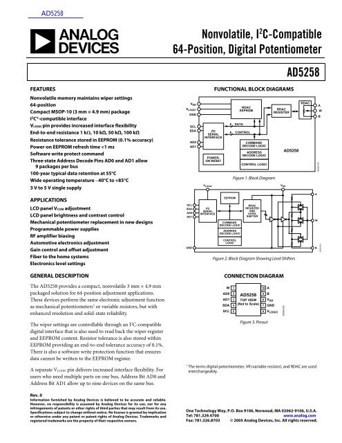
Nonvolatile, I2C-Compatible 64-Position, Digital Potentiometer ...
Nonvolatile, I2C-Compatible 64-Position, Digital Potentiometer ...
Nonvolatile, I2C-Compatible 64-Position, Digital Potentiometer ...

You also want an ePaper? Increase the reach of your titles
YUMPU automatically turns print PDFs into web optimized ePapers that Google loves.
查 询 AD5258 供 应 商<strong>Nonvolatile</strong>, I 2 C-<strong>Compatible</strong><strong>64</strong>-<strong>Position</strong>, <strong>Digital</strong> <strong>Potentiometer</strong>AD5258FEATURES<strong>Nonvolatile</strong> memory maintains wiper settings<strong>64</strong>-positionCompact MSOP-10 (3 mm × 4.9 mm) packageI 2 C®-compatible interfaceVLOGIC pin provides increased interface flexibilityEnd-to-end resistance 1 kΩ, 10 kΩ, 50 kΩ, 100 kΩResistance tolerance stored in EEPROM (0.1% accuracy)Power-on EEPROM refresh time
SPECIFICATIONSELECTRICAL CHARACTERISTICSVDD = VLOGIC = 5 V ± 10%, or 3 V ± 10%; VA = VDD; VB = 0 V; −40°C < TA < +85°C, unless otherwise noted.AD5258Table 1.Parameter Symbol Conditions Min Typ 1 Max UnitDC CHARACTERISTICS: RHEOSTAT MODEResistor Differential Nonlinearity R-DNL RWB, VA = no connect LSB1 kΩ −1.5 ±0.3 +1.510 kΩ/50 kΩ/100 kΩ −0.25 ±0.1 +0.25Resistor Integral Nonlinearity R-INL RWB, VA = no connect LSB1 kΩ −5 ±0.5 +510 kΩ/100 kΩ −0.5 ±0.1 +0.550 kΩ −0.25 ±0.1 +0.25Nominal Resistor ToleranceTA = 25°C, VDD = 5.5 V1 kΩ RAB 0.9 1.5 kΩ10 kΩ/50 kΩ/100 kΩ ∆RAB −30 +30 %Resistance Temperature Coefficient (∆RAB × 10 6 )/(RAB × ∆T) Code = 0x00/0x20 200/15 ppm/°CTotal Wiper Resistance RWB Code = 0x00 75 350 ΩDC CHARACTERISTICS:POTENTIOMETER DIVIDER MODEDifferential Nonlinearity DNL LSB1 kΩ −1 ±0.3 +110 kΩ/50 kΩ/100 kΩ −0.25 ±0.1 +0.25Integral Nonlinearity INL LSB1 kΩ −1 ±0.3 +110 kΩ/50 kΩ/100 kΩ −0.25 ±0.1 +0.25Full-Scale Error VWFSE Code = 0x3F LSB1 kΩ −6 −3 010 kΩ −1 −0.3 050 kΩ/100 kΩ −1 −0.1 0Zero-Scale Error VWZSE Code = 0x00 LSB1 kΩ 0 3 510 kΩ 0 0.3 150 kΩ/100 kΩ 0 0.1 0.5Voltage Divider Temperature(∆VW × 10 6 )/(VW × ∆T) Code = 0x00/0x20 120/15 ppm/°CCoefficientRESISTOR TERMINALSVoltage Range VA, B, W GND VDD VCapacitance A, B CA, B f = 1 MHz, measured to GND,45 pFcode = 0x20Capacitance W CW f = 1 MHz, measured to GND,60 pFcode = 0x20Common-Mode Leakage ICM VA = VB = VDD/2 10 nADIGITAL INPUTS AND OUTPUTSInput Logic High VIH 0.7 × VL VL + 0.5 VInput Logic Low VIL −0.5 0.3 × VL VLeakage Current IIL µASDA, AD0, AD1 VIN = 0 V or 5 V 0.01 ±1SCL – Logic High VIN = 0 V −2.5 −1.4 +1SCL – Logic Low VIN = 5 V 0.01 ±1Input Capacitance CIL 5 pFRev. 0 | Page 3 of 24
AD5258Parameter Symbol Conditions Min Typ 1 Max UnitPOWER SUPPLIESPower Supply Range VDD 2.7 5.5 VPositive Supply Current IDD 0.5 2 µALogic Supply VLOGIC 2.7 5.5 VLogic Supply Current ILOGIC VIH = 5 V or VIL = 0 V 3.5 6 µAProgramming Mode Current (EEPROM) ILOGIC(PROG) VIH = 5 V or VIL = 0 V 35 mAPower Dissipation PDISS VIH = 5 V or VIL = 0 V, VDD = 5 V 20 40 µWPower Supply Rejection Ratio PSRR VDD = +5 V ± 10%, Code = 0x20 ±0.01 ±0.06 %/%DYNAMIC CHARACTERISTICSBandwidth −3 dB BW Code = 0x20RAB = 1 kΩ 18000 kHzRAB = 10 kΩ 1000 kHzRAB = 50 kΩ 190 kHzRAB = 100 kΩ 100 kHzTotal Harmonic Distortion THDW RAB = 10 kΩ, VA = 1 V rms, VB = 0,0.1 %f = 1 kHzVW Settling Time tS RAB = 10 kΩ, VAB = 5 V,500 ns±1 LSB error bandResistor Noise Voltage Density eN_WB RWB = 5 kΩ, f = 1 kHz 9 nV/√Hz1Typical values represent average readings at 25°C and V DD = 5 V.Rev. 0 | Page 4 of 24
AD5258TIMING CHARACTERISTICSVDD = VLOGIC = 5 V ± 10%, or 3 V ± 10%; VA = VDD; VB = 0 V; −40°C < TA < +85°C, unless otherwise noted.Table 2.Parameter Symbol Conditions Min Typ Max UnitI 2 C INTERFACE TIMING CHARACTERISTICSSCL Clock Frequency fSCL 0 400 kHztBUF Bus Free Time between STOP and START t1 1.3 µstHD;STA Hold Time (Repeated START) t2 After this period, the first clock pulse is 0.6 µsgenerated.tLOW Low Period of SCL Clock t3 1.3 µstHIGH High Period of SCL Clock t4 0.6 µstSU;STA Setup Time for Repeated STARTt5 0.6 µsConditiontHD;DAT Data Hold Time t6 0 0.9 µstSU;DAT Data Setup Time t7 100 nstF Fall Time of Both SDA and SCL Signals t8 300 nstR Rise Time of Both SDA and SCL Signals t9 300 nstSU;STO Setup Time for STOP Condition t10 0.6 µsEEPROM Data Storing Time tEEMEM_STORE 26 msEEPROM Data Restoring Time at Power On 1 tEEMEM_RESTORE1 VDD rise time dependant. Measure300 µswithout decoupling capacitors at VDD andGND.EEPROM Data Restoring Time upon Restore tEEMEM_RESTORE2 VDD = 5 V. 300 µsCommand 1EEPROM Data Rewritable Time 2 tEEMEM_REWRITE 540 µsFLASH/EE MEMORY RELIABILITYEndurance 3 100 700 kCyclesData Retention 4 100 Years1During power-up, the output is momentarily preset to midscale before restoring EEPROM content.2Delay time after power-on PRESET prior to writing new EEPROM data.3Endurance is qualified to 100,000 cycles per JEDEC Std. 22 method A117, and is measured at –40°C, +25°C, and +85°C; typical endurance at +25°C is 700,000 cycles.4Retention lifetime equivalent at junction temperature (TJ) = 55°C per JEDEC Std. 22, Method A117. Retention lifetime based on an activation energy of 0.6eV derateswith junction temperature.SCLt 8 tt 6 9t 2 t 3tt 5 t 7 t 104t8 t 9SDAt 1P S P05029-004Figure 4. I 2 C Interface Timing DiagramRev. 0 | Page 5 of 24
AD5258ABSOLUTE MAXIMUM RATINGSTA = 25°C, unless otherwise noted.Table 3.ParameterVDD to GNDVA, VB, VW to GNDIMAXValue−0.3 V to +7 VGND − 0.3 V, VDD + 0.3 VPulsed 1±20 mAContinuous±5 mA<strong>Digital</strong> Inputs and Output Voltage to GND 0 V to +7 VOperating Temperature Range−40°C to +85°CMaximum Junction Temperature (TJMAX) 150°CStorage Temperature−65°C to +150°CLead Temperature (Soldering, 10 sec) 300°CThermal Resistance 2 θJA: MSOP − 10 200°C/W1Maximum terminal current is bounded by the maximum current handling ofthe switches, maximum power dissipation of the package, and maximumapplied voltage across any two of the A, B, and W terminals at a givenresistance.2Package power dissipation = (TJMAX – TA)/θJA.Stresses above those listed under Absolute Maximum Ratingsmay cause permanent damage to the device. This is a stressrating only; functional operation of the device at these or anyother conditions above those indicated in the operationalsection of this specification is not implied. Exposure to absolutemaximum rating conditions for extended periods may affectdevice reliability.ESD CAUTIONESD (electrostatic discharge) sensitive device. Electrostatic charges as high as 4000 V readily accumulate onthe human body and test equipment and can discharge without detection. Although this product featuresproprietary ESD protection circuitry, permanent damage may occur on devices subjected to high energyelectrostatic discharges. Therefore, proper ESD precautions are recommended to avoid performancedegradation or loss of functionality.Rev. 0 | Page 6 of 24
AD5258PIN CONFIGURATION AND FUNCTION DESCRIPTIONSW 1AD0 2AD1 3SDA 4SCL 5AD5258TOP VIEW(Not to Scale)10 A9876BV DDGNDV LOGIC05029-008Figure 5. Pin ConfigurationTable 4. Pin Function DescriptionsPin No. Mnemonic Description1 W W Terminal, GND ≤ VW ≤ VDD.2 ADO Programmable Three-State Address Bit 0 for Multiple Package Decoding. State is registered onpower-up.3 AD1 Programmable Three-State Address Bit 1 for Multiple Package Decoding. State is registered onpower-up.4 SDA Serial Data Input/Output.5 SCL Serial Clock Input. Positive edge triggered.6 VLOGIC Logic Power Supply.7 GND <strong>Digital</strong> Ground.8 VDD Positive Power Supply.9 B B Terminal, GND ≤ VB ≤ VDD.10 A A Terminal, GND ≤ VA ≤ VDD.Rev. 0 | Page 7 of 24
AD5258TYPICAL PERFORMANCE CHARACTERISTICSVDD = VLOGIC = 5.5 V, RAB = 10 kΩ, TA = 25°C, unless otherwise noted.0.50.100.40.08RHEOSTAT MODE INL (LSB)0.30.22.7V0.105.5V–0.1–0.2–0.3–0.4–0.50 8 16 24 65 40 48 56 <strong>64</strong>CODE (Decimal)05029-015POTENTIOMETER MODE DNL (LSB)0.060.040.020–0.02–0.04–0.06–0.08–40°C +25°C+85°C–0.100 8 16 24 65 40 48 56 <strong>64</strong>CODE (Decimal)05029-012Figure 6. R-INL vs. Code vs. Supply VoltageFigure 9. DNL vs. Code vs. Temperature0.250.100.200.08RHEOSTAT MODE DNL (LSB)0.150.100.050–0.05–0.10–0.15–0.205.5V2.7V–0.250 8 16 24 65 40 48 56 <strong>64</strong>CODE (Decimal)Figure 7. R-DNL vs. Code vs. Supply Voltages05029-017POTENTIOMETER MODE INL (LSB)0.060.042.7V0.020–0.025.5V–0.04–0.06–0.08–0.100 8 16 24 65 40 48 56 <strong>64</strong>CODE (Decimal)Figure 10. INL vs. Supply Voltages05029-0110.100.080.100.08POTENTIOMETER MODE INL (LSB)0.060.040.020–0.02–0.04–40°C–0.06–0.08+85°C+25°C–0.100 8 16 24 65 40 48 56 <strong>64</strong>CODE (Decimal)05029-010POTENTIOMETER MODE DNL (LSB)0.060.040.020–0.02–0.04–0.06–0.082.7V5.5V–0.100 8 16 24 65 40 48 56 <strong>64</strong>CODE (Decimal)05029-013Figure 8. INL vs. Code vs. TemperatureFigure 11. DNL vs. Code vs. Supply VoltagesRev. 0 | Page 8 of 24
AD52580.250.50RHEOSTAT MODE INL (LSB)0.200.150.100.050–0.05–0.10–0.15–40°C+85°C+25°CZSE (LSB)0.450.400.350.300.250.200.150.10ZSE @ V DD = 2.7VZSE @ V DD = 5.5V–0.20–0.250 8 16 24 65 40 48 56 <strong>64</strong>CODE (Decimal)Figure 12. R-INL vs. Code vs. Temperature05029-0140.050–40 –20 0 20 40 60 80TEMPERATURE (°C)Figure 15. Zero-Scale Error vs. Temperature05029-0480.250.201RHEOSTAT MODE DNL (LSB)0.150.100.050–0.05–0.10–0.15+25°C–40°C+85°CI DD , SUPPLY CURRENT (µA)V DD = 5.5V–0.20–0.250 8 16 24 65 40 48 56 <strong>64</strong>CODE (Decimal)Figure 13. R-DNL vs. Code vs. Temperature05029-0160.1–40 –20 0 20 40 60 80TEMPERATURE (°C)Figure 16. Supply Current vs. Temperature05029-04506–0.05FSE (LSB)–0.10–0.15–0.20–0.25FSE @ V DD = 5.5V–0.30–0.35FSE @ V DD = 2.7V–0.40–0.45–0.50–40 –20 0 20 40 60 80TEMPERATURE (°C)05029-049I LOGIC , LOGIC SUPPLY CURRENT (µA)5V DD = 5.5V4321V DD = 2.7V0–40 –20 0 20 40 60 80TEMPERATURE (°C)05029-046Figure 14. Full-Scale Error vs. TemperatureFigure 17. Logic Supply Current vs. Temperature vs. VDDRev. 0 | Page 9 of 24
AD5258250120RHEOSTAT MODE TEMPCO (ppm/°C)2001501k10050k5010k0–50100k–100–1500 8 16 24 65 40 48 56 <strong>64</strong>CODE (Decimal)05029-019TOTAL RESISTANCE (kΩ)100k Rt @ V DD = 5.5V100806050k Rt @ V DD = 5.5V4010k Rt @ V DD = 5.5V1k Rt @ V DD = 5.5V200–40 –20 0 20 40 60 80TEMPERATURE (°C)05029-050Figure 18. Rheostat Mode Tempco (ΔRAB ×10 6 )/( RAB × ∆T) vs. CodeFigure 21. Total Resistance vs. Temperature1200POTENTIOMETER MODE TEMPCO (ppm/°C)1008060402050k1k010k100k–200 8 16 24 65 40 48 56 <strong>64</strong>CODE (Decimal)05029-018GAIN (dB)20 H–610 H–1208 H–1804 H02 H–2401 H–30–36–42–48–54–6010k 100k 1M 10M 100MFREQUENCY (Hz)05029-022Figure 19. <strong>Potentiometer</strong> Mode Tempco (ΔVW × 10 6 )/( VW × ΔT) vs. CodeFigure 22. Gain vs. Frequency vs. Code, RAB = 1 kΩ3500300250R WB @ V DD = 2.7V–6–12–1820 H10 H08 HR WB @ 0x00200150GAIN (dB)–24–30–3604 H02 H01 H100–4250R WB @ V DD = 5.5V0–40 –20 0 20 40 60 80TEMPERATURE (°C)Figure 20. RWB vs. Temperature05029-047–48–54–601k 10k 100k 1M 10MFREQUENCY (Hz)Figure 23. Gain vs. Frequency vs. Code, RAB = 10 kΩ05029-023Rev. 0 | Page 10 of 24
AD52580–620 H80CODE = MIDSCALE, V A = V LOGIC , V B = 0V–12–1810 H08 H60PSRR @ V LOGIC = 5V DC ± 10% p-p ACGAIN (dB)–24–30–3604 H02 H01 HPSRR (dB)40PSRR @ V LOGIC = 3V DC ± 10% p-p AC–42–4820–54–601k 10k 100k 1MFREQUENCY (Hz)05029-0240100 1k 10k100k1MFREQUENCY (Hz)05029-056Figure 24. Gain vs. Frequency vs. Code, RAB = 50 kΩFigure 27. PSRR vs. Frequency0–620 HGAIN (dB)–12–18–24–30–36–42–4810 H08 H04 H02 H01 H5V/DIV 500mV/DIV12V WSCL–54–601k 10k 100k 1MFREQUENCY (Hz)05029-025400ns/DIV05029-053Figure 25. Gain vs. Frequency vs. Code, RAB = 100 kΩFigure 28. <strong>Digital</strong> Feedthrough10k1kV DD = V LOGIC = 5VI LOGIC (µA)100V DD = V LOGIC = 3V200mV/DIV1V W100 1 2 3 4 5V IH (V)05029-0521µs/DIV05029-055Figure 26. Logic Supply Current vs. Input VoltageFigure 29. Midscale Glitch, Code 0×7F to 0×80Rev. 0 | Page 11 of 24
AD52585V/DIV 2V/DIV12V WSCL200ns/DIV05029-054Figure 30. Large Signal Settling TimeRev. 0 | Page 12 of 24
AD5258TEST CIRCUITSFigure 31 through Figure 36 illustrate the test circuits thatdefine the test conditions used in the product specificationtables.V+DUTAWBV+ = V DD1LSB = V+/2 NV MS05029-030V+∆V DDV A∆VDUT (MS)AWBV+ = V DD ± 10%PSRR (dB) = 20 LOG∆V∆V MS % DDPSS (%/%) =∆V DD %V MS05029-033Figure 31. Test Circuit for <strong>Potentiometer</strong> Divider Nonlinearity Error (INL, DNL)Figure 34. Test Circuit for Power Supply Sensitivity (PSS, PSSR)NO CONNECTDUTA WBV MSI W05029-031OFFSETGNDV IN+2.5VABDUTW+5VAD8610–5VV OUT05029-034Figure 32. Test Circuit for Resistor <strong>Position</strong> Nonlinearity Error(Rheostat Operation; R-INL, R-DNL)Figure 35. Test Circuit for Gain vs. FrequencyV MS2DUTAWBV WV MS1I W = V DD /R NOMINALR W = [V MS1 – V MS2 ]/I W05029-032DUTWR SW = 0.1V I SWCODE = 0x000.1VI SWBGND TO V DD05029-035Figure 33. Test Circuit for Wiper ResistanceFigure 36. Test Circuit for Common-Mode Leakage CurrentRev. 0 | Page 13 of 24
AD5258THEORY OF OPERATIONThe AD5258 is a <strong>64</strong>-position digitally controlled variableresistor (VR) device. The wiper’s default value, prior toprogramming the EEPROM, is midscale.PROGRAMMING THE VARIABLE RESISTORRheostat OperationThe nominal resistance (RAB) of the RDAC between Terminal Aand Terminal B is available in 1 kΩ, 10 kΩ, 50 kΩ, and 100 kΩ.The nominal resistance of the VR has <strong>64</strong> contact pointsaccessed by the wiper terminal. The 6-bit data in the RDAClatch is decoded to select one of <strong>64</strong> possible settings.ABWABFigure 37. Rheostat Mode ConfigurationThe general equation determining the digitally programmedoutput resistance between Wiper W and Terminal B isDR WB×<strong>64</strong>( D) = × RAB+ 2 RWwhere:D is the decimal equivalent of the binary code loaded in the6-bit RDAC register.RAB is the end-to-end resistance.RW is the wiper resistance contributed by the on resistance ofeach internal switch.D5D4D3D2D1D0RDACLATCHANDDECODERR SR SR SR SFigure 38. AD5258 Equivalent RDAC CircuitNote that in the zero-scale condition, there is a relatively lowvalue finite wiper resistance. Care should be taken to limit thecurrent flow between Wiper W and Terminal B in this state to amaximum pulse current of no more than 20 mA. Otherwise,degradation or destruction of the internal switch contact canoccur.WABAWBW05029-03705029-036(1)Similar to the mechanical potentiometer, the resistance of theRDAC between Wiper W and Terminal A produces a digitallycontrolled complementary resistance, RWA. The resistance valuesetting for RWA starts at a maximum value of resistance anddecreases as the data loaded in the latch increases in value. Thegeneral equation for this operation is<strong>64</strong> − DRWA( D)= × RAB+ 2 × R(2)W<strong>64</strong>Typical device-to-device matching is process lot dependent andmay vary by up to ±30%. For this reason, resistance tolerance isstored in the EEPROM such that the user will know the actualRAB within 0.1%.PROGRAMMING THE POTENTIOMETER DIVIDERVoltage Output OperationThe digital potentiometer easily generates a voltage divider atWiper W-to-Terminal B and Wiper W-to-Terminal A proportionalto the input voltage at Terminal A to Terminal B. Unlikethe polarity of VDD to GND, which must be positive, voltageacross Terminal A to Terminal B, Wiper W to Terminal A, andWiper W to Terminal B can be at either polarity.V IABWV OFigure 39. <strong>Potentiometer</strong> Mode ConfigurationIf ignoring the effect of the wiper resistance for approximation,connecting the A terminal to 5 V and the B terminal to groundproduces an output voltage at Wiper W-to-Terminal B startingat 0 V up to 1 LSB less than 5 V. The general equation definingthe output voltage at VW with respect to ground for any validinput voltage applied to Terminal A and Terminal B isD <strong>64</strong> − DVW( D)= VA+ V(3)B<strong>64</strong> <strong>64</strong>A more accurate calculation, which includes the effect of wiperresistance, VW, isR ( D)RV ( D)+W( D)WBWA= VAVB(4)RABRABOperation of the digital potentiometer in the divider moderesults in a more accurate operation over temperature. Unlikethe rheostat mode, the output voltage is dependent mainly onthe ratio of the Internal Resistors, RWA and RWB, and not theabsolute values.05029-038Rev. 0 | Page 14 of 24
AD5258I 2 C INTERFACENote that the wiper’s default value, prior to programming theEEPROM, is midscale.1. The master initiates data transfer by establishing a STARTcondition when a high-to-low transition on the SDA lineoccurs while SCL is high (see Figure 4). The next byte isthe slave address byte, which consists of the slave address(first 7 bits) followed by an R/W bit (see Table 6). When theR/W bit is high, the master reads from the slave device.When the R/W bit is low, the master writes to the slavedevice.The slave address of the part is determined by two threestate-configurableAddress Pins AD0 and AD1. The state ofthese two pins is registered upon power-up and decodedinto a corresponding I 2 C 7-bit address (see Table 5). Theslave address corresponding to the transmitted address bitsresponds by pulling the SDA line low during the ninthclock pulse (this is termed the slave acknowledge bit).At this stage, all other devices on the bus remain idle whilethe selected device waits for data to be written to, or readfrom, its serial register.2. Writing: In the write mode, the last bit (R/W) of the slaveaddress byte is logic low. The second byte is the instructionbyte. The first three bits of the instruction byte are thecommand bits (see Table 6). The user must choose whetherto write to the RDAC register, EEPROM register, oractivate the software write protect (see Table 7 to Table 10).The final five bits are all zeros (see Table 13 to Table 14).The slave again responds by pulling the SDA line low duringthe ninth clock pulse.The final byte is the data byte MSB first. Don’t cares can beleft either high or low. In the case of the write protectmode, data is not stored; rather, a logic high in the LSBenables write protect. Likewise, a logic low will disablewrite protect. The slave again responds by pulling the SDAline low during the ninth clock pulse.3. Storing/Restoring: In this mode, only the address andinstruction bytes are necessary. The last bit (R/W) of theaddress byte is logic low. The first three bits of theinstruction byte are the command bits (see Table 6). Thetwo choices are transfer data from RDAC to EEPROM(store), or from EEPROM to RDAC (restore). The final fivebits are all zeros (see Table 13 to Table 14).4. Reading: Assuming the register of interest was not justwritten to, it is necessary to write a dummy address andinstruction byte. The instruction byte will vary dependingon whether the data that is wanted is the RDAC register,EEPROM register, or tolerance register (see Table 11 toTable 16).After the dummy address and instruction bytes are sent, arepeat start is necessary. After the repeat start, anotheraddress byte is needed, except this time the R/W bit is logichigh. Following this address byte is the readback bytecontaining the information requested in the instructionbyte. Read bits appear on the negative edges of the clock.Don’t cares may either be in a high or low state.The tolerance register can be read back individually (seeTable 15) or consecutively (see Table 16). Refer to the ReadModes section for detailed information on the interpretationof the tolerance bytes.5. After all data bits have been read or written, a STOPcondition is established by the master. A STOP condition isdefined as a low-to-high transition on the SDA line whileSCL is high. In write mode, the master pulls the SDA linehigh during the tenth clock pulse to establish a STOPcondition (see Figure 45). In read mode, the master issues ano acknowledge for the ninth clock pulse (that is, the SDAline remains high). The master then brings the SDA linelow before the tenth clock pulse, and then raises SDA highto establish a STOP condition (see Figure 46).A repeated write function gives the user flexibility toupdate the RDAC output a number of times afteraddressing and instructing the part only once. Forexample, after the RDAC has acknowledged its slaveaddress and instruction bytes in the write mode, the RDACoutput is updated on each successive byte until a STOPcondition is received. If different instructions are needed,the write/read mode has to start again with a new slaveaddress, instruction, and data byte. Similarly, a repeatedread function of the RDAC is also allowed.Rev. 0 | Page 15 of 24
AD5258I 2 C BYTE FORMATSThe following generic, write, read, and store/restore controlregisters for the AD5258 all refer to the device addresses listedin Table 5, and the mode/condition reference key (S, P, SA, MA,NA, W, R, and X) listed below.S = Start ConditionP = Stop ConditionSA = Slave AcknowledgeMA = Master AcknowledgeNA = No AcknowledgeTable 5. Device Address LookupAD1 and AD0 are three-state address pins.Device Address AD1 AD00011000 0 00011001 NC 00011010 1 00101001 0 NC0101010 NC NC0101011 1 NC1001100 0 11001101 NC 11001110 1 1W = WriteR = ReadX = Don’t CareGENERIC INTERFACETable 6. Generic Interface Format7-Bit Device AddressS (See Table 5) R/W SA C2 C1 C0 A4 A3 A2 A1 A0 SA D7 D6 D5 D4 D3 D2 D1 D0 SA PSlave Address Byte Instruction Byte Data ByteTable 7. RDAC-to-EEPROM Interface Command DescriptionsC2 C1 C0 Command Description0 0 0 Operation between I 2 C and RDAC0 0 1 Operation between I 2 C and EEPROM0 1 0 Operation between I 2 C and Write ProtectionRegister. See Table 10.1 0 0 NOP1 0 1 Restore EEPROM to RDAC1 1 0 Store RDAC to EEPROMRev. 0 | Page 16 of 24
AD5258WRITE MODESTable 8. Writing to RDAC RegisterS7-Bit Device Address(See Table 5) 0 SA 0 0 0 0 0 0 0 0 SA X X D5 D4 D3 D2 D1 D0 SA PSlave Address Byte Instruction Byte Data ByteTable 9. Writing to EEPROM RegisterS7-Bit Device Address(See Table 5) 0 SA 0 0 1 0 0 0 0 0 SA X X D5 D4 D3 D2 D1 D0 SA PSlave Address Byte Instruction Byte Data ByteThe wiper’s default value, prior to programming the EEPROM, is midscale.Table 10. Activating/Deactivating Software Write ProtectS7-Bit Device Address(See Table 5) 0 SA 0 1 0 0 0 0 0 0 SA 0 0 0 0 0 0 0 WP SA PSlave Address Byte Instruction Byte Data ByteIn order to activate the write protection mode, the WP bit in Table 10 must be logic high. In order to deactivate the write protection, thecommand must be sent again except with the WP in logic zero state.READ MODESRead modes are referred to as traditional because the first twobytes for all three cases are “dummy” bytes which function toplace the pointer towards the correct register. This is the reasonfor the repeat start. In theory, this step can be avoided if theuser is interested in reading a register that was previouslywritten to. For example, if the EEPROM was just written to,then the user can skip the two dummy bytes and proceeddirectly to the slave address byte followed by the EEPROMreadback data.Table 11. Traditional Readback of RDAC Register Value7-Bit Device AddressS (See Table 5) 0 SA 0 0 0 0 0 0 0 0 SA S7-Bit Device Address(See Table 5) 1 SA X X D5 D4 D3 D2 D1 D0 NA PSlave Address Byte Instruction Byte Slave Address Byte Read Back Data↑Repeat startTable 12. Traditional Readback of Stored EEPROM Value7-Bit Device AddressS (See Table 5) 0 SA 0 0 1 0 0 0 0 0 SA S7-Bit Device Address(See Table 5) 1 SA X X D5 D4 D3 D2 D1 D0 NA PSlave Address Byte Instruction Byte Slave Address Byte Read Back Data↑Repeat startSTORE/RESTORE MODESTable 13. Storing RDAC Value to EEPROM7-Bit Device AddressS (See Table 5) 0 SA 1 1 0 0 0 0 0 0 SA PSlave Address Byte Instruction ByteTable 14. Restoring EEPROM to RDAC7-Bit Device AddressS (See Table 5) 0 SA 1 0 1 0 0 0 0 0 SA PSlave Address Byte Instruction ByteRev. 0 | Page 17 of 24
AD5258TOLERANCE READBACK MODESTable 15. Traditional Readback of Tolerance (Individually)S7-Bit Device Address(See Table 5)0 SA 0 0 1 1 1 1 1 0 SA S7-Bit Device Address(See Table 5)1SAD7D6D5D4D3D2D1D0NA PSlave Address Byte Instruction Byte Slave Address Byte Sign + Integer Byte↑Repeat startS7-Bit Device Address(See Table 5)0 SA 0 0 1 1 1 1 1 1 SA S7-Bit Device Address(See Table 5)1SAD7D6D5D4D3D2D1D0NA PSlave Address Byte Instruction Byte Slave Address Byte Decimal Byte↑Repeat startTable 16.Traditional Readback of Tolerance (Consecutively)S7-Bit Device Address(See Table 5)0 SA 0 0 1 1 1 1 1 0 SA S7-Bit Device Address(See Table 5)1 SA D7 D6 D5 D4 D3 D2 D1 D0 MA D7 D6 D5 D4 D3 D2 D1 D0 NA PSlave Address Byte Instruction Byte Slave Address Byte Sign + Integer Byte Decimal Byte↑Repeat startCalculating R AB Tolerance Stored in Read-Only MemoryA D7 D6 D5 D4 D3 D2 D1 D0 A D7 D6 D5 D4 D3 D2 D1 D0 ASIGN 2 6 2 5 2 4 2 3 2 2 2 1 2 0 2 –1 2 –2 2 –3 2 –4 2 –5 2 –6 2 –7 2 –8SIGN7 BITS FOR INTEGER NUMBER8 BITS FOR DECIMAL NUMBER05029-005Figure 40. Format of Stored Tolerance in Sign Magnitude Format with Bit <strong>Position</strong> Descriptions.(Unit is Percent. Only Data Bytes are Shown.)The AD5258 features a patented RAB tolerance storage in thenonvolatile memory. The tolerance is stored in the memoryduring factory production and can be read by users at any time.The knowledge of stored tolerance allows users to accuratelycalculate RAB. This feature is valuable for precision, rheostatmode, and open-loop applications where knowledge of absoluteresistance is critical.The stored tolerance resides in the read-only memory and isexpressed as a percentage. The tolerance is stored in two memorylocation bytes in sign magnitude binary form (see Figure 40).The two EEPROM address bytes are 11110 (sign + integer) and11111 (decimal number). The two bytes can be individuallyaccessed with two separate commands (see Table 15). Alternatively,readback of the first byte followed by the second byte can bedone in one command (see Table 16). In the latter case, thememory pointer will automatically increment from the first tothe second EEPROM location (increments from 11110 to11111) if read consecutively.In the first memory location, the MSB is designated for the sign(0 = + and 1= –) and the seven LSBs are designated for the integerportion of the tolerance. In the second memory location, all eightdata bits are designated for the decimal portion of tolerance. Notethat the decimal portion has a limited accuracy of only 0.1%. Forexample, if the rated RAB = 10 kΩ and the data readback fromAddress 11110 shows 0001 1100, and Address 11111 shows0000 1111, then the tolerance can be calculated asMSB: 0 = +Next 7 MSB: 001 1100 = 288 LSB: 0000 1111 = 15 × 2 –8 = 0.06Tolerance = +28.06%Rounded Tolerance = +28.1% and therefore,RAB_ACTUAL = 12.810 kΩRev. 0 | Page 18 of 24
AD5258ESD PROTECTION OF DIGITAL PINS ANDRESISTOR TERMINALSThe AD5258 VDD, VLOGIC, and GND power supplies define theboundary conditions for proper 3-terminal and digital inputoperation. Supply signals present on Terminal A, Terminal B,and Terminal W that exceed VDD or GND are clamped by theinternal forward biased ESD protection diodes (see Figure 41).<strong>Digital</strong> Input SCL and <strong>Digital</strong> Input SDA are clamped by ESDprotection diodes with respect to VLOGIC and GND as shown inFigure 42.V DDSimilarly, it is also good practice to bypass the power supplieswith quality capacitors for optimum stability. Supply leads tothe device should be bypassed with disc or chip ceramiccapacitors of 0.01 µF to 0.1 µF. Low ESR 1 µF to 10 µF tantalumor electrolytic capacitors should also be applied at the suppliesto minimize any transient disturbance and low frequency ripple(see Figure 43). The digital ground should also be joinedremotely to the analog ground at one point to minimize theground bounce.V DDC210µF+C10.1µFV DDAD5258AWBGNDFigure 41. Maximum Terminal Voltages Set by VDD and GNDV LOGICSCLSDAGNDFigure 42. Maximum Terminal Voltages Set by VLOGIC and GNDPOWER-UP SEQUENCEBecause the ESD protection diodes limit the voltage complianceat Terminal A, Terminal B, and Terminal W (see Figure 41), it isimportant to power GND/VDD/VLOGIC before applying anyvoltage to Terminal A, Terminal B, and Terminal W; otherwise,the diode is forward biased such that VDD and VLOGIC arepowered unintentionally and may affect the user’s circuit. Theideal power-up sequence is in the following order: GND, VDD,VLOGIC, digital inputs, and then VA, VB, VW. The relative order ofpowering VA, VB, VW, and the digital inputs is not important aslong as they are powered after GND/VDD/VLOGIC.05029-03905029-040GNDFigure 43. Power Supply BypassingMULTIPLE DEVICES ON ONE BUSThe AD5258 has two three-state configurable Address PinsAD0 and AD1. The state of these two pins is registered uponpower-up and decoded into a corresponding I 2 C 7-bit address(see Table 5). This allows up to nine devices on the bus to bewritten to, or read from, independently. In the case that the pinis assigned to be floated, the static voltage will be VLOGIC/2.EVALUATION BOARDAn evaluation board, along with all necessary software, isavailable to program the AD5258 from any PC runningWindows® 98/2000/XP. The graphical user interface, as shownin Figure 44, is straightforward and easy to use. More detailedinformation is available in the user manual that comes with theboard.05029-041LAYOUT AND POWER SUPPLY BYPASSINGIt is good practice to employ compact, minimum lead lengthlayout design. The leads to the inputs should be as direct aspossible with minimum conductor length. Ground paths shouldhave low resistance and low inductance.Figure 44. AD5258 Evaluation Board Software05029-042Rev. 0 | Page 19 of 24
AD5258DISPLAY APPLICATIONSCIRCUITRYA special feature of the AD5258 is its unique separation of theVLOGIC and VDD supply pins. The reason for doing this is toprovide greater flexibility in applications that do not alwaysprovide needed supply voltages.In particular, LCD panels often require a VCOM voltage in therange of 3 V to 5 V. The circuit in Figure 45 is the rare exceptionin which a 5 V supply is available to power the digitalpotentiometer.VDD will not affect that node’s bias because it is only on theorder of microamps. VLOGIC is tied to the MCU’s 3.3 V digitalsupply because VLOGIC will draw the 35 mA which is neededwhen writing to the EEPROM. It would be impractical to tryand source 35 mA through the 70 kΩ resistor, therefore, VLOGICis not connected to the same node as VDD.For this reason, VLOGIC and VDD are provided as two separatesupply pins that can either be tied together or treated independently;VLOGIC supplying the logic/EEPROM with power,and VDD biasing up the A, B, and W terminals for addedflexibility.C11µFVCC (~3.3V)MCUR610kΩR510kΩ5VAD5258V DDV LOGICSCLSDAGND14.4VABR170kΩR210kΩWR325kΩ–U1AD8565Figure 45. VCOM Adjustment Application+3.5V < V COM < 4.5V05029-006C11µFVCC (~3.3V)MCUR610kΩSUPPLIES POWERTO BOTH THEMICRO AND THELOGIC SUPPLY OFTHE DIGITAL POTR510kΩAD5258V DDV LOGICSCLSDAGND14.4VABR170kΩR210kΩWR325kΩ–U1AD8565+3.5V < V COM < 4.5VFigure 46. Circuitry When a Separate Supply is Not Available for VDD05029-007In the more common case shown in Figure 46, only analog 14.4 Vand digital logic 3.3 V supplies are available. By placing discreteresistors above and below the digital pot, VDD can now be tappedoff the resistor string itself. Based on the chosen resistor values,the voltage at VDD in this case equals 4.8 V, allowing the wiper tobe safely operated all the way up to 4.8 V. The current draw ofFor a more detailed look at this application, refer to the article,“Simple VCOM Adjustment uses any Logic Supply Voltage” inthe September 30, 2004, issue of EDN magazine.Rev. 0 | Page 20 of 24
AD5258OUTLINE DIMENSIONS3.00 BSC3.00 BSC10 <strong>64</strong>.90 BSC15PIN 10.50 BSC0.950.850.750.150.000.270.17COPLANARITY0.101.10 MAXSEATINGPLANE0.230.088°0°0.800.600.40COMPLIANT TO JEDEC STANDARDS MO-187BAFigure 47. 10-Lead Mini Small Outline Package [MSOP](RM-10)Dimensions shown in millimetersORDERING GUIDEModel RAB (Ω) Temperature Package Description Package Option BrandingAD5258BRMZ1 1 1 k –40°C to +85°C MSOP-10 RM-10 D4KAD5258BRMZ1-R7 1 1 k –40°C to +85°C MSOP-10 RM-10 D4KAD5258BRMZ10 1 10 k –40°C to +85°C MSOP-10 RM-10 D4LAD5258BRMZ10-R7 1 10 k –40°C to +85°C MSOP-10 RM-10 D4LAD5258BRMZ50 1 50 k –40°C to +85°C MSOP-10 RM-10 D4MAD5258BRMZ50-R7 1 50 k –40°C to +85°C MSOP-10 RM-10 D4MAD5258BRMZ100 1 100 k –40°C to +85°C MSOP-10 RM-10 D4NAD5258BRMZ100-R7 1 100 k –40°C to +85°C MSOP-10 RM-10 D4NAD5258EVAL 2 Evaluation Board1Z = Pb-free part.2The evaluation board is shipped with the 10 kΩ RAB resistor option; however, the board is compatible with all available resistor value options.Rev. 0 | Page 21 of 24
AD5258NOTESRev. 0 | Page 22 of 24
AD5258NOTESRev. 0 | Page 23 of 24
AD5258NOTES2 2Purchase of licensed I C components of Analog Devices or one of its sublicensed Associated Companies conveys a license for the purchaser under the Philips I C PatentRights to use these components in an I C system, provided that the system conforms to the I C Standard Specification as defined by Philips2 2.© 2005 Analog Devices, Inc. All rights reserved. Trademarks andregistered trademarks are the property of their respective owners.D05029–0–3/05(0)Rev. 0 | Page 24 of 24

![P-CAD EDA - [Sheet1]](https://img.yumpu.com/49470492/1/190x115/p-cad-eda-sheet1.jpg?quality=85)