Nonvolatile, I2C-Compatible 64-Position, Digital Potentiometer ...
Nonvolatile, I2C-Compatible 64-Position, Digital Potentiometer ...
Nonvolatile, I2C-Compatible 64-Position, Digital Potentiometer ...

You also want an ePaper? Increase the reach of your titles
YUMPU automatically turns print PDFs into web optimized ePapers that Google loves.
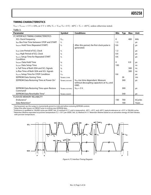
AD5258TIMING CHARACTERISTICSVDD = VLOGIC = 5 V ± 10%, or 3 V ± 10%; VA = VDD; VB = 0 V; −40°C < TA < +85°C, unless otherwise noted.Table 2.Parameter Symbol Conditions Min Typ Max UnitI 2 C INTERFACE TIMING CHARACTERISTICSSCL Clock Frequency fSCL 0 400 kHztBUF Bus Free Time between STOP and START t1 1.3 µstHD;STA Hold Time (Repeated START) t2 After this period, the first clock pulse is 0.6 µsgenerated.tLOW Low Period of SCL Clock t3 1.3 µstHIGH High Period of SCL Clock t4 0.6 µstSU;STA Setup Time for Repeated STARTt5 0.6 µsConditiontHD;DAT Data Hold Time t6 0 0.9 µstSU;DAT Data Setup Time t7 100 nstF Fall Time of Both SDA and SCL Signals t8 300 nstR Rise Time of Both SDA and SCL Signals t9 300 nstSU;STO Setup Time for STOP Condition t10 0.6 µsEEPROM Data Storing Time tEEMEM_STORE 26 msEEPROM Data Restoring Time at Power On 1 tEEMEM_RESTORE1 VDD rise time dependant. Measure300 µswithout decoupling capacitors at VDD andGND.EEPROM Data Restoring Time upon Restore tEEMEM_RESTORE2 VDD = 5 V. 300 µsCommand 1EEPROM Data Rewritable Time 2 tEEMEM_REWRITE 540 µsFLASH/EE MEMORY RELIABILITYEndurance 3 100 700 kCyclesData Retention 4 100 Years1During power-up, the output is momentarily preset to midscale before restoring EEPROM content.2Delay time after power-on PRESET prior to writing new EEPROM data.3Endurance is qualified to 100,000 cycles per JEDEC Std. 22 method A117, and is measured at –40°C, +25°C, and +85°C; typical endurance at +25°C is 700,000 cycles.4Retention lifetime equivalent at junction temperature (TJ) = 55°C per JEDEC Std. 22, Method A117. Retention lifetime based on an activation energy of 0.6eV derateswith junction temperature.SCLt 8 tt 6 9t 2 t 3tt 5 t 7 t 104t8 t 9SDAt 1P S P05029-004Figure 4. I 2 C Interface Timing DiagramRev. 0 | Page 5 of 24

![P-CAD EDA - [Sheet1]](https://img.yumpu.com/49470492/1/190x115/p-cad-eda-sheet1.jpg?quality=85)