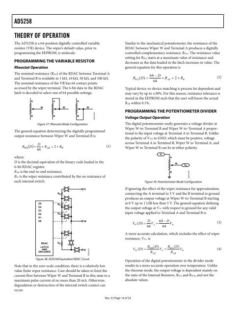
AD5258THEORY OF OPERATIONThe AD5258 is a <strong>64</strong>-position digitally controlled variableresistor (VR) device. The wiper’s default value, prior toprogramming the EEPROM, is midscale.PROGRAMMING THE VARIABLE RESISTORRheostat OperationThe nominal resistance (RAB) of the RDAC between Terminal Aand Terminal B is available in 1 kΩ, 10 kΩ, 50 kΩ, and 100 kΩ.The nominal resistance of the VR has <strong>64</strong> contact pointsaccessed by the wiper terminal. The 6-bit data in the RDAClatch is decoded to select one of <strong>64</strong> possible settings.ABWABFigure 37. Rheostat Mode ConfigurationThe general equation determining the digitally programmedoutput resistance between Wiper W and Terminal B isDR WB×<strong>64</strong>( D) = × RAB+ 2 RWwhere:D is the decimal equivalent of the binary code loaded in the6-bit RDAC register.RAB is the end-to-end resistance.RW is the wiper resistance contributed by the on resistance ofeach internal switch.D5D4D3D2D1D0RDACLATCHANDDECODERR SR SR SR SFigure 38. AD5258 Equivalent RDAC CircuitNote that in the zero-scale condition, there is a relatively lowvalue finite wiper resistance. Care should be taken to limit thecurrent flow between Wiper W and Terminal B in this state to amaximum pulse current of no more than 20 mA. Otherwise,degradation or destruction of the internal switch contact canoccur.WABAWBW05029-03705029-036(1)Similar to the mechanical potentiometer, the resistance of theRDAC between Wiper W and Terminal A produces a digitallycontrolled complementary resistance, RWA. The resistance valuesetting for RWA starts at a maximum value of resistance anddecreases as the data loaded in the latch increases in value. Thegeneral equation for this operation is<strong>64</strong> − DRWA( D)= × RAB+ 2 × R(2)W<strong>64</strong>Typical device-to-device matching is process lot dependent andmay vary by up to ±30%. For this reason, resistance tolerance isstored in the EEPROM such that the user will know the actualRAB within 0.1%.PROGRAMMING THE POTENTIOMETER DIVIDERVoltage Output OperationThe digital potentiometer easily generates a voltage divider atWiper W-to-Terminal B and Wiper W-to-Terminal A proportionalto the input voltage at Terminal A to Terminal B. Unlikethe polarity of VDD to GND, which must be positive, voltageacross Terminal A to Terminal B, Wiper W to Terminal A, andWiper W to Terminal B can be at either polarity.V IABWV OFigure 39. <strong>Potentiometer</strong> Mode ConfigurationIf ignoring the effect of the wiper resistance for approximation,connecting the A terminal to 5 V and the B terminal to groundproduces an output voltage at Wiper W-to-Terminal B startingat 0 V up to 1 LSB less than 5 V. The general equation definingthe output voltage at VW with respect to ground for any validinput voltage applied to Terminal A and Terminal B isD <strong>64</strong> − DVW( D)= VA+ V(3)B<strong>64</strong> <strong>64</strong>A more accurate calculation, which includes the effect of wiperresistance, VW, isR ( D)RV ( D)+W( D)WBWA= VAVB(4)RABRABOperation of the digital potentiometer in the divider moderesults in a more accurate operation over temperature. Unlikethe rheostat mode, the output voltage is dependent mainly onthe ratio of the Internal Resistors, RWA and RWB, and not theabsolute values.05029-038Rev. 0 | Page 14 of 24
AD5258I 2 C INTERFACENote that the wiper’s default value, prior to programming theEEPROM, is midscale.1. The master initiates data transfer by establishing a STARTcondition when a high-to-low transition on the SDA lineoccurs while SCL is high (see Figure 4). The next byte isthe slave address byte, which consists of the slave address(first 7 bits) followed by an R/W bit (see Table 6). When theR/W bit is high, the master reads from the slave device.When the R/W bit is low, the master writes to the slavedevice.The slave address of the part is determined by two threestate-configurableAddress Pins AD0 and AD1. The state ofthese two pins is registered upon power-up and decodedinto a corresponding I 2 C 7-bit address (see Table 5). Theslave address corresponding to the transmitted address bitsresponds by pulling the SDA line low during the ninthclock pulse (this is termed the slave acknowledge bit).At this stage, all other devices on the bus remain idle whilethe selected device waits for data to be written to, or readfrom, its serial register.2. Writing: In the write mode, the last bit (R/W) of the slaveaddress byte is logic low. The second byte is the instructionbyte. The first three bits of the instruction byte are thecommand bits (see Table 6). The user must choose whetherto write to the RDAC register, EEPROM register, oractivate the software write protect (see Table 7 to Table 10).The final five bits are all zeros (see Table 13 to Table 14).The slave again responds by pulling the SDA line low duringthe ninth clock pulse.The final byte is the data byte MSB first. Don’t cares can beleft either high or low. In the case of the write protectmode, data is not stored; rather, a logic high in the LSBenables write protect. Likewise, a logic low will disablewrite protect. The slave again responds by pulling the SDAline low during the ninth clock pulse.3. Storing/Restoring: In this mode, only the address andinstruction bytes are necessary. The last bit (R/W) of theaddress byte is logic low. The first three bits of theinstruction byte are the command bits (see Table 6). Thetwo choices are transfer data from RDAC to EEPROM(store), or from EEPROM to RDAC (restore). The final fivebits are all zeros (see Table 13 to Table 14).4. Reading: Assuming the register of interest was not justwritten to, it is necessary to write a dummy address andinstruction byte. The instruction byte will vary dependingon whether the data that is wanted is the RDAC register,EEPROM register, or tolerance register (see Table 11 toTable 16).After the dummy address and instruction bytes are sent, arepeat start is necessary. After the repeat start, anotheraddress byte is needed, except this time the R/W bit is logichigh. Following this address byte is the readback bytecontaining the information requested in the instructionbyte. Read bits appear on the negative edges of the clock.Don’t cares may either be in a high or low state.The tolerance register can be read back individually (seeTable 15) or consecutively (see Table 16). Refer to the ReadModes section for detailed information on the interpretationof the tolerance bytes.5. After all data bits have been read or written, a STOPcondition is established by the master. A STOP condition isdefined as a low-to-high transition on the SDA line whileSCL is high. In write mode, the master pulls the SDA linehigh during the tenth clock pulse to establish a STOPcondition (see Figure 45). In read mode, the master issues ano acknowledge for the ninth clock pulse (that is, the SDAline remains high). The master then brings the SDA linelow before the tenth clock pulse, and then raises SDA highto establish a STOP condition (see Figure 46).A repeated write function gives the user flexibility toupdate the RDAC output a number of times afteraddressing and instructing the part only once. Forexample, after the RDAC has acknowledged its slaveaddress and instruction bytes in the write mode, the RDACoutput is updated on each successive byte until a STOPcondition is received. If different instructions are needed,the write/read mode has to start again with a new slaveaddress, instruction, and data byte. Similarly, a repeatedread function of the RDAC is also allowed.Rev. 0 | Page 15 of 24


![P-CAD EDA - [Sheet1]](https://img.yumpu.com/49470492/1/190x115/p-cad-eda-sheet1.jpg?quality=85)