Wideband Gain Block Amplifier Design Techniques
Wideband Gain Block Amplifier Design Techniques
Wideband Gain Block Amplifier Design Techniques

You also want an ePaper? Increase the reach of your titles
YUMPU automatically turns print PDFs into web optimized ePapers that Google loves.
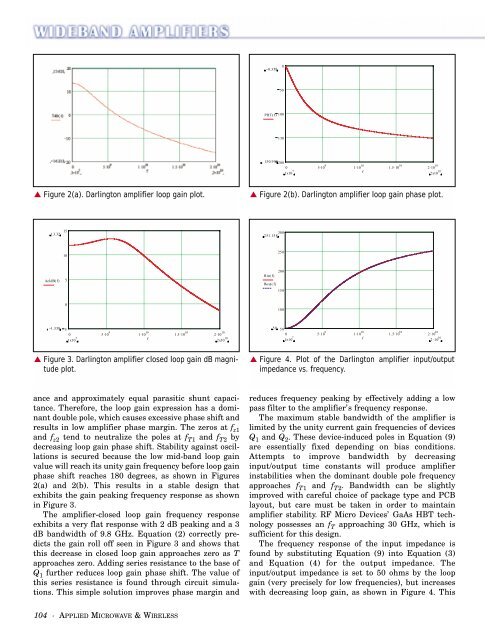
−0.358050PHT( f)100150150.9992000 5. 10 9 1 . 10 10 1.5 . 10 10 2 . 10 10110 x7f2x10 10▲ Figure 2(a). Darlington amplifier loop gain plot.▲ Figure 2(b). Darlington amplifier loop gain phase plot.1513.32300251.15810250AcldB( f)5Rin( f)Ro ut ( f)2001500100−1.35850 5 . 10 9 1 . 10 10 1.5 . 10 10 2 . 10 10110 x7f210 x1050 50110 x7 f 210 100 5 10 9 1 10 10 1.5 . 10 10 2 . 10 10▲ Figure 3. Darlington amplifier closed loop gain dB magnitudeplot.▲ Figure 4. Plot of the Darlington amplifier input/outputimpedance vs. frequency.ance and approximately equal parasitic shunt capacitance.Therefore, the loop gain expression has a dominantdouble pole, which causes excessive phase shift andresults in low amplifier phase margin. The zeros at f z1and f z2 tend to neutralize the poles at f T1 and f T2 bydecreasing loop gain phase shift. Stability against oscillationsis secured because the low mid-band loop gainvalue will reach its unity gain frequency before loop gainphase shift reaches 180 degrees, as shown in Figures2(a) and 2(b). This results in a stable design thatexhibits the gain peaking frequency response as shownin Figure 3.The amplifier-closed loop gain frequency responseexhibits a very flat response with 2 dB peaking and a 3dB bandwidth of 9.8 GHz. Equation (2) correctly predictsthe gain roll off seen in Figure 3 and shows thatthis decrease in closed loop gain approaches zero as Tapproaches zero. Adding series resistance to the base ofQ 1 further reduces loop gain phase shift. The value ofthis series resistance is found through circuit simulations.This simple solution improves phase margin andreduces frequency peaking by effectively adding a lowpass filter to the amplifier’s frequency response.The maximum stable bandwidth of the amplifier islimited by the unity current gain frequencies of devicesQ 1 and Q 2 . These device-induced poles in Equation (9)are essentially fixed depending on bias conditions.Attempts to improve bandwidth by decreasinginput/output time constants will produce amplifierinstabilities when the dominant double pole frequencyapproaches f T1 and f T2 . Bandwidth can be slightlyimproved with careful choice of package type and PCBlayout, but care must be taken in order to maintainamplifier stability. RF Micro Devices’ GaAs HBT technologypossesses an f T approaching 30 GHz, which issufficient for this design.The frequency response of the input impedance isfound by substituting Equation (9) into Equation (3)and Equation (4) for the output impedance. Theinput/output impedance is set to 50 ohms by the loopgain (very precisely for low frequencies), but increaseswith decreasing loop gain, as shown in Figure 4. This104 · APPLIED MICROWAVE & WIRELESS

![P-CAD EDA - [Sheet1]](https://img.yumpu.com/49470492/1/190x115/p-cad-eda-sheet1.jpg?quality=85)