Wideband Gain Block Amplifier Design Techniques
Wideband Gain Block Amplifier Design Techniques
Wideband Gain Block Amplifier Design Techniques

You also want an ePaper? Increase the reach of your titles
YUMPU automatically turns print PDFs into web optimized ePapers that Google loves.
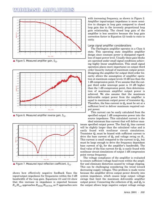
dB (S (2, 1))12.011.511.010.510.09.59.08.58.0with increasing frequency, as shown in Figure 2.<strong>Amplifier</strong> input/output impedance is more sensitiveto changes in loop gain compared to closedloop gain due to the inversely proportional loopgain relationship. The closed loop gain of theamplifier is less sensitive because the loop gaincorrection factor in Equation (2) tends to ratio tounity.7.57.06.56.00 1 2 3 4 5 6 7 8 9 10 11 12fre q , GHz▲ Figure 5. Measured amplifier gain, S 21 .d B(S (1, 2))-13.6-13.8-14.0-14.2-14.4-14.6-14.8-15.0-15.2-15.4-15.6-15.8-16.0-16.20 1 2 3 4 5 6 7 8 9 10 11 12freq, GHz▲ Figure 6. Measured amplifier reverse gain, S 12 .dB (S (1, 1))-5-10-15-20-25-30-35-40-450 1 2 3 4 5 6 7 8 9 10 11 12fre q , GHz▲ Figure 7. Measured input reflection coefficient, S 11 .shows how effectively negative feedback fixes theinput/output impedance for frequencies within the 3 dBbandwidth of the loop gain. Equations (3) and (4) showthat this increase in impedance is expected becauseR in /R out approaches R INOL /R OUTOL as T approaches zeroLarge signal amplifier considerationsThe Darlington amplifier operates in a Class Astate. This operating state simplifies amplifierdesign since constant power is dissipated regardlessof input power level. Usually these gain blocksare operated under small signal conditions achievinghighly linear amplification. This small signaloperation places more importance on output thirdorder linearity instead of maximum output power.<strong>Design</strong>ing the amplifier for output third order linearityallows the assumption of amplifier operationat maximum output levels 10 dB less than the1 dB compression point. If we assume that the outputthird order intercept point is 10 dB higherthan the 1 dB compression point, then determinationof maximum amplifier output power isachieved. We also assume that the maximumdeliverable output power from the amplifier isequal to maximum output power of transistor Q 2 .Therefore, the bias current in Q 2 must be set at asufficient level to deliver maximum required outputpower.This current can be easily calculated from thespecified output 1 dB compression power into thesource impedance. This calculated current is theideal minimum bias current that will deliver maximumspecified output power. The final Q 2 bias currentwill be slightly larger than the calculated value and iseasily found with nonlinear circuit simulations.Transistor Q 1 must be biased with sufficient current todrive the base current of Q 2 and voltage swing on R 1 .This current is small compared to the current in Q 2 , butmust be large enough to drive the frequency dependantbase current of Q 2 for the amplifier’s bandwidth. Thefinal value of the bias current for Q 1 is easily found withnonlinear circuit simulations of output 1 dB compressionpoint versus frequency.The voltage compliance of the amplifier is evaluatedto ensure sufficient voltage head room within the amplifierand eliminate distortion caused by voltage clipping.This can be challenging considering the trend towarddecreasing supply voltages. This problem is made worsebecause the amplifier drives output power directly intosystem impedance, which causes large output voltageswings that limit the maximum deliverable amplifieroutput power. Connecting the collectors of Q 1 and Q 2 tothe output allows large negative output voltage swingsAPRIL 2001 · 105

![P-CAD EDA - [Sheet1]](https://img.yumpu.com/49470492/1/190x115/p-cad-eda-sheet1.jpg?quality=85)