Analysis and design of a 200W LDMOS based doherty amplifier for ...
Analysis and design of a 200W LDMOS based doherty amplifier for ...
Analysis and design of a 200W LDMOS based doherty amplifier for ...

Create successful ePaper yourself
Turn your PDF publications into a flip-book with our unique Google optimized e-Paper software.
WE5A-3<br />
<strong>Analysis</strong> <strong>and</strong> Design <strong>of</strong> a <strong>200W</strong> <strong>LDMOS</strong> Based<br />
Doherty Amplifier <strong>for</strong> 3G Base Stations<br />
John R. Gajadharsing, Ol<strong>of</strong> Bosma*, <strong>and</strong> Pim van Westen*<br />
Philips Semiconductors, BU Mobile Communications, Nijmegen, The Netherl<strong>and</strong>s<br />
*MAP, Meerlaan 21, 1671 ED, Medemblik, The Netherl<strong>and</strong>s<br />
Abstract - In tbis paper the analy& <strong>and</strong> <strong>design</strong> <strong>of</strong> a<br />
2OOW classical Doherty <strong>amplifier</strong> is described using dlscrete<br />
<strong>LDMOS</strong> devices. The peak (class-C) <strong>and</strong> main (class-AB)<br />
<strong>amplifier</strong>s are desigbed with two stages to obtain flat AM-<br />
AM <strong>and</strong> AM-PM charPCteristics <strong>for</strong> the Doherty <strong>amplifier</strong>.<br />
An asymmetrical planar coupler structure is uWed as an<br />
input splitter <strong>and</strong> microship <strong>based</strong> elements are used <strong>for</strong><br />
phase matching <strong>and</strong> power combloing at the output. Thh<br />
Doherty PA has a measured PldB <strong>of</strong> 53dBm <strong>and</strong> exhibits an<br />
efiiciency <strong>of</strong> 34% at 6dB back<strong>of</strong>f (47") <strong>for</strong> two-carrier<br />
WCDMA. The ACPR <strong>and</strong> IM3 obtained at 47dBm are 37dBc<br />
<strong>and</strong> 33dBc respectively. The gain at 6dB back<strong>of</strong>f is ZZdB over<br />
the frequency range 2.11-2.17GHz Design considerations <strong>for</strong><br />
a Doherty ampMer <strong>based</strong> on discrete <strong>LDMOS</strong> devices are<br />
addressed.<br />
Index terms - Doherty, <strong>LDMOS</strong>, AM-AM, AM-PM,<br />
WCDMA, power amplifiem<br />
I. INTRODUCTION<br />
In contemporary base stations <strong>amplifier</strong> <strong>design</strong>s <strong>for</strong><br />
WCDMA, one <strong>of</strong> the main concerns is the power<br />
consumption. Due to the linearity requirements the<br />
operating point <strong>of</strong> these <strong>amplifier</strong>s are constrained to the<br />
backdff region where it is not most efficient. Although<br />
we can still expect to see @proved back<strong>of</strong>f efficiency<br />
through advancement in device technology it is<br />
theoretically limited. The Doherty <strong>amplifier</strong> is a technique<br />
<strong>for</strong> improving the efficiency <strong>of</strong> backed-<strong>of</strong>f <strong>amplifier</strong>s<br />
beyond the limits <strong>of</strong> conventional <strong>amplifier</strong>s.<br />
In this paper we will discuss a <strong>200W</strong> <strong>amplifier</strong> <strong>design</strong><br />
<strong>for</strong> WCDMA that has a significantly improved efficiency<br />
in the back<strong>of</strong>f region using discrete <strong>LDMOS</strong> devices.<br />
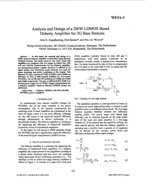
(PAZ) <strong>amplifier</strong>, typically biased in class AB <strong>and</strong> C<br />
respectively, with their outputs connected by an<br />
impedance inverter, usually a quarter-wave transmission<br />
line. The delay introduced by this N4 line is compensated<br />
by a N4 delay in the input path to PA2 to ensure that the<br />
correct phase relationship is restored.<br />
Input 4<br />
Peak<br />
"DD<br />
Fig. 1 Topology <strong>of</strong> a two stage Dohem.<br />
The <strong>amplifier</strong>s operation is well described hy Raab [2]<br />
In essence an active load-pulling effect is created as each<br />
<strong>amplifier</strong> tums on at different power levels. The two-stage<br />
Doherty <strong>amplifier</strong> there<strong>for</strong>e exhibits two efficiency<br />
peaking points. The power range over which high<br />
efficiency can be obtained depends on the peak power<br />
ratio <strong>of</strong> the main <strong>and</strong> peak <strong>amplifier</strong> in a two-stage<br />
Doherty [2]. If we assume that the <strong>amplifier</strong>s utilized, are<br />
ideal class-B devices <strong>and</strong> that the Doherty <strong>amplifier</strong> is<br />
operating into a resistive load, a general set <strong>of</strong> equations<br />
can be derived <strong>for</strong> the currents, power levels <strong>and</strong><br />
efficiency as function <strong>of</strong> the output voltage:<br />
11. Two STAGE DOHERR &VIEW<br />
The Doherty <strong>amplifier</strong> is a technique <strong>for</strong> improving the<br />
efficiency <strong>of</strong> backed-<strong>of</strong>f linear <strong>amplifier</strong>s. In a Doherty<br />
<strong>amplifier</strong>, the output powers <strong>of</strong> two <strong>amplifier</strong>s operating at<br />
a proper phase alignment <strong>and</strong> bias level, are combined<br />
using appropriate power combining techniques [l]. The<br />
topology <strong>of</strong> this so called two-stage Doherty <strong>amplifier</strong> is<br />
shown in Figure 1. It consists <strong>of</strong> a main (PAl) <strong>and</strong> peak<br />
0-7803-8331-1/04/$20.00 Q 2004 IEEE<br />
529<br />
2004 IEEE MTT-S Digest
The individual power levels as indicated in Fig.] are<br />
plotted (4)
e lost when the Doherty <strong>amplifier</strong> is operating below its<br />
transition point. It is there<strong>for</strong>e necessary to add a driver<br />
stage to maximize efficiency. A driver is also added to the<br />
main <strong>amplifier</strong> to accommodate shaping <strong>of</strong> the transfer<br />
characteristics, which is critical in a Doherty <strong>amplifier</strong>.<br />
The splitter asymmetry (A) is set by the gain difference:<br />
A=G,-G, (9)<br />
The gain <strong>of</strong> the total Doherty <strong>amplifier</strong>, at full power, can<br />
then be determined from:<br />
Gm, - 3 +GI - IOlog(l+ (10)<br />
In order to maintain a constant gain over power <strong>for</strong> the<br />
total Doherty <strong>amplifier</strong>, the gain characteristics (AWAM)<br />
<strong>of</strong> the peak <strong>amplifier</strong> should be matched to that <strong>of</strong> the<br />
main <strong>amplifier</strong>, <strong>and</strong>,can be determined from:<br />
G, = 101og(lO"'lo(l+ IOd~~o)-lOG1po)- A (1 1)<br />
The <strong>amplifier</strong>s are <strong>design</strong>ed using internally matched<br />
Philips <strong>LDMOS</strong> transistors. In order to get maximum<br />
efficiency improvement in a Doherty <strong>amplifier</strong> the<br />
transistors need to have specific properties. The transistor<br />
<strong>for</strong> the peak <strong>amplifier</strong> should he <strong>design</strong>ed to have a high<br />
<strong>of</strong>f-state output impedance <strong>and</strong> exhibit low reverse RF<br />
drive. For the main <strong>amplifier</strong> the transistor should he able<br />
to provide maximum per<strong>for</strong>mance under the load pulling<br />
conditions.<br />
The implementation <strong>of</strong> the two-stage class-AB main<br />
<strong>amplifier</strong>, using two BLF2022-40 (5OWpeak) in the final<br />
stage <strong>and</strong> one BLF2043(10W) in the driver stage, is<br />
shown in Fig. 5. The final stage devices are paralleled<br />
without using a quadrature combiner, since both<br />
transistors must experience in-phase load-pulling <strong>for</strong><br />
Doherty operation. The interstage matching is <strong>design</strong>ed to<br />
meet the b<strong>and</strong>width requirement <strong>of</strong> 60MHz <strong>and</strong> to obtain<br />
approximately 3dB compression required <strong>for</strong> Doherty<br />
operation.<br />
Fig. 5. Class-AB main <strong>amplifier</strong> implementation.<br />
The resulting M AM <strong>and</strong> AMPM characteristics <strong>for</strong> a<br />
50n load are shown in Fig. 6 with a peak power capability<br />
<strong>of</strong> 1oow.<br />
Poldhl<br />
Fig. 6. AM-AM <strong>and</strong> AM-PM characteristics <strong>of</strong> the class-AB<br />
main <strong>amplifier</strong> <strong>for</strong> a 5011 load:<br />
The implementation <strong>of</strong> the two-stage class-C peak<br />
<strong>amplifier</strong> is shown in Fig. 7. It utilizes two BLF2022-40 in<br />
the final stage <strong>and</strong> one similar device in the driver stage.<br />
The interstage circuit not only provides impedance<br />
matching but also the correct phase matching between the<br />
driver output <strong>and</strong> final stage input in order to obtain a<br />
predistortion effect that aligns the M AM <strong>and</strong> AM/PM<br />
characteristics <strong>of</strong> the peak <strong>amplifier</strong> with main <strong>amplifier</strong>.<br />
The resulting M AM <strong>and</strong> AWM characteristics <strong>for</strong> a<br />
50n load are shown in Fig. 8 with a peak power capability<br />
<strong>of</strong> 1oow.<br />
Fig. 7. Class-C peak <strong>amplifier</strong> implementation.<br />
X I I I I I I I -,&a<br />
0 . . . . .. . .. .. . . -155<br />
a11 21 zs a U 24 xi Y U) e " 48 4a a U<br />
hldbl<br />
Fig. 8. AM-AM <strong>and</strong> AM-PM characteristics <strong>of</strong> the class-C peak<br />
<strong>amplifier</strong> <strong>for</strong> a 5On load.<br />
Fig. 9 shows the circuit diagram <strong>of</strong> the total Doberty<br />
implementation. The transmission lines TL3 <strong>and</strong> TL4 are<br />
used to maximize overall efficiency. TL3 provides the<br />
phase matching to rotate the <strong>of</strong>f-state impedance <strong>of</strong> the<br />
peak <strong>amplifier</strong> to a high impedance level at the combining<br />
point between TL5 <strong>and</strong> TL6. TL4 provides the phase<br />
matching to ensure that a resistive load <strong>of</strong> twice the<br />
nominal value is presented at the die level <strong>of</strong> the main PA<br />
transistors. The input utilizes an asymmetrical (5dB)<br />
branch line coupler as a splitter. TLl <strong>and</strong> TJ2 are added to<br />
53 1
~<br />
~~~ .,<br />
~~ .<br />
ensure that the output arrive in phase at the combining<br />
point.<br />
IM3 obtained at 47dBm are 37dBc <strong>and</strong> 33dBc<br />
respectively. The gain at 6dB back-<strong>of</strong>f is 22dB over the<br />
frequency range 2.11-2.17GHz.<br />
x1<br />
21:<br />
. ~<br />
. ~~,~<br />
.............<br />
Fig. 9. Schematic <strong>of</strong> the Dohaty implementation.<br />
SCC<br />
c<br />
The AMIAM <strong>and</strong> AM/F’M characteristics <strong>of</strong> the total<br />
Doherty system are shown in Fig. 10. The contribution <strong>of</strong><br />
the peak <strong>amplifier</strong> becomes significant above 48dBm.<br />
4 10<br />
>3 15<br />
n r)<br />
P : ::<br />
137<br />
I8 %i<br />
-10<br />
-3s<br />
a<br />
S D Y S X I ~ 4 U I I B B Y<br />
”1-1<br />
Fig. IO. AM-AM <strong>and</strong> AM-PM characteristics <strong>of</strong> the total<br />
Doherty <strong>amplifier</strong>.<br />
,I<br />
I<br />
Y a I<br />
U,., 47 50 53<br />
Fig. 11. CW gain <strong>and</strong> efficiency <strong>of</strong> the total Doherty <strong>amplifier</strong> at<br />
t 2.14GHz.<br />
:li.<br />
g15<br />
5 ( 0<br />
1~ ~-~ .<br />
. ~<br />
i\;<br />
I_ ma 1Dx) m 2130 ma 2

![P-CAD EDA - [Sheet1]](https://img.yumpu.com/49470492/1/190x115/p-cad-eda-sheet1.jpg?quality=85)