Lab 5: Op Amps II and Introduction to Phase-Locked Loops 5.1 ...
Lab 5: Op Amps II and Introduction to Phase-Locked Loops 5.1 ...
Lab 5: Op Amps II and Introduction to Phase-Locked Loops 5.1 ...

Create successful ePaper yourself
Turn your PDF publications into a flip-book with our unique Google optimized e-Paper software.
<strong>Lab</strong> 5: <strong>Op</strong> <strong>Amps</strong> <strong>II</strong> <strong>and</strong><br />
<strong>Introduction</strong> <strong>to</strong> <strong>Phase</strong>-<strong>Locked</strong> <strong>Loops</strong><br />
<strong>5.1</strong> Goals of this <strong>Lab</strong><br />
Further exploration of operational amplier characteristics <strong>and</strong> associated feedbacknetworks.<br />
In the second part, a dierent type of feedback loop is utilized in a phase-locked loop circuit.<br />
The connections for the model 741 or 411 integrated circuit op-amps used in our labs are<br />
shown below in Fig. 1.<br />
Figure 1: 8-pin DIP package connections for 741 or 411 op-amps.<br />
5.2 Integra<strong>to</strong>r<br />
Construct the integra<strong>to</strong>r/low-pass lter circuit shown in Fig. 2. Start with a 741 op-amp.<br />
Use a large ( 0:2 <strong>to</strong>1F) unpolarized capaci<strong>to</strong>r for C <strong>and</strong> let R i = 100 k.<br />
C<br />
R i<br />
V<br />
2<br />
in<br />
3<br />
1<br />
10 k<br />
-<br />
741/411<br />
+<br />
5<br />
6<br />
V out<br />
-15 V<br />
Figure 2: Active integra<strong>to</strong>r.<br />
5.2.1<br />
We begin by studying op-amp drifting. Connect the input <strong>to</strong> ground. While looking at the<br />
output with the oscilloscope, initialize the integra<strong>to</strong>r by shorting the capaci<strong>to</strong>r by momentarily<br />
putting a1kresis<strong>to</strong>racross it. After removing the resis<strong>to</strong>r you will probably observe<br />
1
the output level drifting. Even if the oset voltage has been carefully zeroed (using the oset<br />
balance control via pins 1 <strong>and</strong> 5), the output will drift due <strong>to</strong> oset currents. Note the rate<br />
of drift in volts per second. Try adjusting the oset voltage balance <strong>to</strong> see if this can alter<br />
the rate of drift.<br />
5.2.2<br />
Now replace the 741 with a 411 op-amp. The 411 has JFET inputs, with huge input<br />
impedance. The rate of output drift should improve. If the drift is still noticeable, try<br />
placing a large ( 10 M) resis<strong>to</strong>r in parallel with C. Continue with the 411 for the remaining<br />
exercises.<br />
5.2.3<br />
Input a small DC voltage (using, for example, the oset control of the function genera<strong>to</strong>r).<br />
Try a few values of R i <strong>and</strong> C <strong>to</strong> verify that the output ramp rate is indeed controlled by the<br />
product R i C.<br />
5.2.4<br />
Input a variety ofwaveforms <strong>and</strong> draw the input <strong>and</strong> output. Is this a good integra<strong>to</strong>r<br />
Being sure not <strong>to</strong> drive the op-amp in<strong>to</strong> saturation, you can use the scope AC input if oset<br />
drift continues <strong>to</strong> be a problem. Vary the frequency of an input sine wave <strong>and</strong> compare the<br />
ratio of output <strong>to</strong> input amplitudes over a wide frequency range.<br />
5.3 Dierentia<strong>to</strong>r<br />
Construct the circuit shown in Fig. 3. The role of the 100 pF capaci<strong>to</strong>r has <strong>to</strong> do with roll-o<br />
stability (see text page 224) <strong>and</strong> should otherwise be ignorable. Input a sine wave of about<br />
100 Hz <strong>and</strong> vary its gain. Is the gain linear with frequency as would be expected for a true<br />
dierentia<strong>to</strong>r If the same R = 10k <strong>and</strong> C =0:1F were used for a passive dierentia<strong>to</strong>r,<br />
at about what frequency would it fail How does that compare with the op-amp version<br />
100 pF<br />
10 k<br />
V in<br />
2<br />
0.1 MF<br />
3<br />
-<br />
+<br />
6<br />
V out<br />
Figure 3: Active dierentia<strong>to</strong>r.<br />
5.3.1<br />
Input a triangle wave. Note the square-wave output, as expected. Is the square wave perfectly<br />
sharp How might the high-frequency response be improved by modifying the circuit Try<br />
it.<br />
2
<strong>Introduction</strong> <strong>to</strong> <strong>Phase</strong>-<strong>Locked</strong> <strong>Loops</strong><br />
The phase-locked loop (PLL) circuit has an enormous number of important applications,<br />
including signal (FM) modulation/demodulation, synchronization <strong>and</strong> replication of weak<br />
signals (e.g. the \lock-in amplier"), <strong>and</strong> frequency multiplication <strong>and</strong> synthesis. Here, we<br />
hope <strong>to</strong> set up a PLL circuit <strong>and</strong> <strong>to</strong> gain some intuition for PLL operation. We will do this<br />
with a circuit which uses the PLL as a frequency multiplier. To begin, our input will be at<br />
about 60 Hz. Generating multiples of the 60 Hz line frequency is commonly used for noise<br />
reduction (due <strong>to</strong> AC power interference) <strong>and</strong> other techniques.<br />
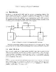
Schematically, the PLL circuit looks like that shown in Fig. 4.<br />
f<br />
in<br />
<strong>Phase</strong><br />
Detec<strong>to</strong>r<br />
Low-pass<br />
Filter<br />
f<br />
replica<br />
Counter<br />
(divide by n)<br />
VCO<br />
(V->f)<br />
f out<br />
V out<br />
Figure 4: PLL schematic with frequency multiplication.<br />
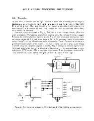
5.4 Frequency Multiplier<br />
The circuit of Fig. 5 is a realization of the general scheme of Fig. 4. Each 4046 PLL chip<br />
includes phase detec<strong>to</strong>rs (2 types) <strong>and</strong> a VCO. (A VCO, or voltage-controlled oscilla<strong>to</strong>r, is a<br />
device which produces an output square wave for which the frequency is proportional <strong>to</strong> an<br />
input voltage.) So, although it is shown functionally as two blocks in the gure, both blocks<br />
are on the same IC. See the attached data sheets for more detail <strong>and</strong> pin assignments. (The<br />
4046 includes an XOR gate phase detec<strong>to</strong>r (Type I) output at pin 2 <strong>and</strong> a state machine<br />
phase detec<strong>to</strong>r (Type <strong>II</strong>) at pin 13. We will be using the Type <strong>II</strong>.)<br />
The 4040 is a 12-stage ripple counter. We will use this <strong>to</strong> provide the divide-by-n function.<br />
We will set this up initially with the output taken at Q 10 , as shown, which represents a divide<br />
by n =2 10 = 1024. That is, for every 2 10 input pulses, the counter produces one output<br />
pulse at pin Q 10 .<br />
5.4.1<br />
Construct the circuit of Fig. 5. Use the function genera<strong>to</strong>r <strong>to</strong> provide a 60 Hz square wave<br />
input with high level (logical TRUE) of 4{5 V <strong>and</strong> low level (logical FALSE) of 0{1 V. Using<br />
the oscilloscope, compare the input <strong>and</strong> your PLL replica which is input at pin 3 of the 4046.<br />
How long does it take the PLL <strong>to</strong> achieve a stable replica When this occurs, the PLL is<br />
\locked" <strong>and</strong> the LED should turn on. Do the two signals, f in <strong>and</strong> its replica, have the same<br />
frequency <strong>and</strong> phase<br />
3
LED "Lock"<br />
470pF<br />
2.2k<br />
+5 V<br />
1<br />
6 7 11 16<br />
f<br />
in<br />
1k<br />
14<br />
Type I 2<br />
4<br />
VCO<br />
4046 4046<br />
Out<br />
3 13<br />
4.7M<br />
Type <strong>II</strong><br />
9<br />
1uF<br />
5 8<br />
330k<br />
R<br />
14 3<br />
Q10<br />
11<br />
Q5<br />
4040<br />
Counter<br />
16 8<br />
10<br />
+5 V<br />
Figure 5: PLL circuit.<br />
5.4.2<br />
Slowly change the frequency of the input. Does the replica follow itTry abruptly changing<br />
the input frequency. How long does it take before the PLL locks again This can be<br />
altered by changing the damping resis<strong>to</strong>r: Change the 330k resis<strong>to</strong>r <strong>to</strong> 33k <strong>and</strong> measure<br />
(approximately) the change in time <strong>to</strong> lock. Change it back when you are done.<br />
5.4.3<br />
Measure the frequency at the output of the VCO using the osciloscope.<br />
expected<br />
Is it what you<br />
5.5 Exp<strong>and</strong>ed Lock Range<br />
Take the replica signal from the Q 5 output, rather than Q 10 of the 4040 counter, so that<br />
now n =2 5<br />
= 32. In order <strong>to</strong> maintain constant loop gain, the damping resis<strong>to</strong>r (330k) must<br />
provide increased attenuation by the same fac<strong>to</strong>r as the ratio of frequencies. Hence, change<br />
it <strong>to</strong> 10k. With this conguration, your PLL should now be able <strong>to</strong> achievelockover a much<br />
wider range of input frequency. Measure this range. Would this be sucient <strong>to</strong> demodulate<br />
audio signals for FM radio (Recall that the audio range is roughly 20 Hz <strong>to</strong> 20 kHz.)<br />
4