Lab 3: Transistor Circuits and JFETs This Lab is Too Long by 50 3.1 ...
Lab 3: Transistor Circuits and JFETs This Lab is Too Long by 50 3.1 ...
Lab 3: Transistor Circuits and JFETs This Lab is Too Long by 50 3.1 ...

You also want an ePaper? Increase the reach of your titles
YUMPU automatically turns print PDFs into web optimized ePapers that Google loves.
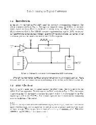
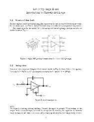
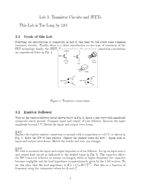
<strong>Lab</strong> 3: <strong>Trans<strong>is</strong>tor</strong> <strong>Circuits</strong> <strong>and</strong> <strong>JFETs</strong><strong>Th<strong>is</strong></strong> <strong>Lab</strong> <strong>is</strong> <strong>Too</strong> <strong>Long</strong> <strong>by</strong> <strong>50</strong>%<strong>3.1</strong> Goals of th<strong>is</strong> <strong>Lab</strong>Following our introduction to trans<strong>is</strong>tors in <strong>Lab</strong> 2, th<strong>is</strong> time we will study some commontrans<strong>is</strong>tor circuits. Finally, there <strong>is</strong> a short introduction to one type of trans<strong>is</strong>tor of theFET technology family, the JFET. For convenience, the trans<strong>is</strong>tor connection conventionsare reproduced below in Fig. 1.Figure 1: <strong>Trans<strong>is</strong>tor</strong> connections.3.2 Emitter FollowerWire up the emitter follower circuit shown below inFig.2. Inputasinewave with amplitudesymmetric about ground. Compare input <strong>and</strong> output of your follower. Increase the inputamplitude beyond 5 V. Sketch the input <strong>and</strong> output wave forms.3.2.1Replace the emitter res<strong>is</strong>tor connection to ground with a connection to ,15 V, as shown inFig. 3. Keep the 270 base res<strong>is</strong>tor. (Ignore the dashed boxes for now.) Again look atinput <strong>and</strong> output wave forms. Sketch the results <strong>and</strong> note any changes.3.2.2We w<strong>is</strong>h to measure the input <strong>and</strong> output impedances of our follower. Set up an input source<strong>and</strong> output load circuit as indicated <strong>by</strong> the dashed boxes in Fig. 3. The capacitor allowsthe DC trans<strong>is</strong>tor behavior to remain unchanged, while at higher frequency the capacitorbecomes negligible <strong>and</strong> the load impedance <strong>is</strong> approximately given <strong>by</strong> the 1 k res<strong>is</strong>tor. Tosee th<strong>is</strong> show that the load impedance <strong>is</strong> R [1 + 1=(!RC) 2 ] 1=2 . Plot th<strong>is</strong> as a function offrequency using the component values for R <strong>and</strong> C.1
+15 V2702N3904Vin3.3kVoutFigure 2: Basic emitter follower.+15 VVin10 k2N39043.3kVout+3.3 MF1 k-15 VFigure 3: Symmetric follower with input (source) <strong>and</strong> output (load) stages shown in thedashed-line boxes.2
To measure Z out ,we consider the Thevenin equivalent circuit with the load, cons<strong>is</strong>ting ofthe 1 k load in parallel with the 3:3 k emitter res<strong>is</strong>tor, in series with Z out , hence formingavoltage divider. Operating at a frequency well above ! 3db of the load, measure the outputamplitude with <strong>and</strong> without the 1 k load to determine Z out .To measure Z in , remove the load. The entire follower now represents an impedance Z inin series with the 10 k source res<strong>is</strong>tor. Hence, <strong>by</strong> measuring the signal amplitude on eachside of the 10 k res<strong>is</strong>tor, we can determine Z in .<strong>Th<strong>is</strong></strong>may be dicult to measure.An important point of the emitter follower <strong>is</strong> that it represents a large input impedance<strong>and</strong> a small output impedance. The input impedance <strong>is</strong> about Z in Z load , whereas Z out Z source =, where Z load <strong>is</strong> the load to be driven <strong>by</strong> the emitter-follower including any emitterres<strong>is</strong>tor (3:3 k here), <strong>and</strong> Z source <strong>is</strong> the source impedance of the signal being delivered tothe emitter-follower. Do these expectations agree with your measurements ?3.3 Current SourceThe arrangement shown in Fig. 4 (left) can serve asanapproximate current source. Usethe 10 k variable res<strong>is</strong>tor on your prototype board as the load to be driven <strong>by</strong> the currentsource. Again, measure the collector current delivered to the load <strong>by</strong> the voltage drop acrossthe 1 k res<strong>is</strong>tor. Starting with the highest value, vary (slowly!) the load res<strong>is</strong>tance whilemeasuring the current. How good <strong>is</strong> th<strong>is</strong> current source? At whatvalue of R does thedelivered current deviate <strong>by</strong> more than 20% from the initial value?+15 V+15 V1k6.8 k(load) R0.25 MF56 kVoutVin2N3904+5 V4702N39045.6k820680Figure 4: A simple current source (left), <strong>and</strong> a common emitter amplier (right).3.4 Common-emitter AmplierSet up the common-emitter amplier shown in Fig. 4 (right). Input a small-amplitude sinewave. Measure the voltage gain of the amplier V out =V in over the frequency range <strong>50</strong> Hz to10 kHz. Make a rough plot of gain versus log 10 of frequency. What <strong>is</strong> the measured ! 3dbpoint? Does th<strong>is</strong> agree with your expectation?3
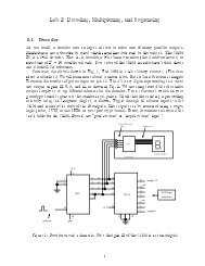
+ 15 VV in0.01 MF2N5485V out1 M 4.7 kFigure 6: Basic JFET source follower.5