Lab 2: Decoding, Multiplexing, and Sequencing 2.1 Decoder
Lab 2: Decoding, Multiplexing, and Sequencing 2.1 Decoder
Lab 2: Decoding, Multiplexing, and Sequencing 2.1 Decoder

Create successful ePaper yourself
Turn your PDF publications into a flip-book with our unique Google optimized e-Paper software.
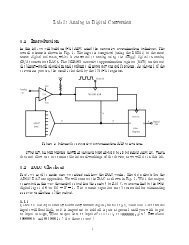
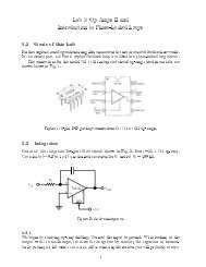
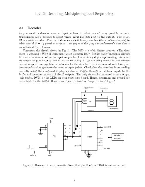
<strong>Lab</strong> 2: <strong>Decoding</strong>, <strong>Multiplexing</strong>, <strong>and</strong> <strong>Sequencing</strong><strong>2.1</strong> <strong>Decoder</strong>As you recall, a decoder uses an input address to select one of many possible outputs.Multiplexers use a decoder to select which input line gets sent to the output. The 74154IC is a 4-bit decoder. That is, it decodes a 4-bit binary number (the 4 address inputs) toselect one of 2 4 = 16 possible outputs. Two pages of the 74154 manufacturer's data sheetsare attached, for reference.Construct the circuit shown in Fig. 1. The 7493 is a 4-bit binary counter. (The datasheet is attached.) We will learn more about counters later. But its basic function is simple:It counts the number of pulses input on pin 14. The 4 binary digits representing this countare output on pins 12, 9, 8, <strong>and</strong> 11, as shown in Fig. 1. We are using these 4 bits of counteroutput simply to set up dierent adresses for the decoder. Use a debounced switch onyourprototype board to generate the counter input pulses. Check that the counting is proceedingcorrectly using the 7-segment display, asshown. Toggle through all address inputs to the74154 <strong>and</strong> measure the state of the 16 outputs. The outputs can be measured using a scope,logic probe, DVM, or the LEDs on your prototype board. Hence, determine <strong>and</strong> record thetruth table for the 74154. Does it use \positive true" or \negative true" logic ?binary (BCD) input4 bits 7 outputs (a-g)a0a1a2a37447circuit board7-segment display+5 V57274931189121a3a2a1a0202122237415417 output 1514 etc13113 etcLED logicindicators14+5 V2421output 0pulse ingnd1012 18 19Figure 1: <strong>Decoder</strong> circuit schematic. Note that pin 12 of the 74154 is not an output.1
2.2 SequencerA sequencer is a decoder for which the input is incremented sequentially by a counter. Thesequence can continuously repeated by resetting the counter. Hence, this is functionally thesame as the previous circuit, except now we will include a \programmable" reset function.In addition, we will change from a binary (i.e. unsigned binary) counter <strong>and</strong> decoder toa BCD counter (7490) <strong>and</strong> decimal decoder (7442). This is shown in Fig. 2. The pinassignments are similar, but not identical, to the previous circuit.Any one of the decoder outputs can be inverted <strong>and</strong> sent to the counter reset (pin 2),as shown. If, for example, output channel n = 5 (of the channels 0{9) is connected to thecounter reset, what will be the highest count that you see on the 7-segment display? Whyis the 7404 inverter needed?binary (BCD) input4 bits 7 outputs (a-g)a0a1a2a37447circuit board7-segment display+5 V5gnd7118a3a2121311 output 99 a1 147490 12 a0 15 74421109714+5 Vgnd1683 etc 21output 0102pulse ingnd217404Figure 2: Sequencer circuit schematic. Note that pin 8 of the 7442 is not an output. Be sureto connect the reset of the 7490 (pin 2) via a 7404 inverter, as shown.2.<strong>2.1</strong>Now connect up the circuit of Fig. 2. Does it work as expected? Vary the position of theconnection to the reset <strong>and</strong> determine the maximum <strong>and</strong> minimum number of channelswhich can be sequenced.2
2.3 Demultiplexerdata in12logicswitchesa2a1a0131415744211 output 91097LED logic3 etc output 0indicators+5 Vgnd16821Figure 3: Demultiplexer circuit schematic.Consider Fig. 3. While a decoder is often used as part of a multiplexer, in this con-guration the 7442 decoder becomes a 1 ! 8demultiplexer. Recall that a demultiplexer(\DEMUX") routes data on a single input to one of several possible output locations, asselected by an input address. In this case, the three least-signicant address bit inputs areused to select the output location, while the most-signicant bit (MSB) at pin 12 becomesthe data input. The data gets routed to output lines 0 to 7. To see how thisworks, examinethe 7442 truth table shown below inTable 2. It uses \negative true" logic for the outputs,but in the table (from the manufacturer) 0 =LOW <strong>and</strong> 1 =HIGH. We see that when the MSB(\D") is LOW, the output selected by the other three bits is LOW, <strong>and</strong> vice versa.Construct the circuit shown in Fig. 3. Use a slow ( 1 Hz) TTL square wave as the datainput. Select an output channel using logic switches. Connect the outputs 0{7 to the 8 logicLEDs on your prototype board. Does the input data appear at the selected output? Whatappears at the other channels? Repeat with a dierent channel.3
2.4 Multiplexer-demultiplexerHere we will construct the circuit of Fig. 4, which consists of a multiplexer (74150) whichsends data to a demultiplexer (74154) over a single line. Hence the two devices communicatevia a serial data link. Sending data over such a serial link clearly saves making manyconnections, which is of practical importance. The MUX <strong>and</strong> DEMUX use the 4-bit addressbus shown in Fig. 4 to communicate whichdatachannel is active. In your circuit, the addresscode will be selected using a counter (7493), as was done earlier. Again, the 7-segment displayis used to display this address.+5 V10725118binary (BCD) input4 bits 7 outputs (a-g)74939121a0a1a2a374477-segment displayaddress select in14circuit board+5 V24data indata in 15data in 01617etc22231etc787415024 9 12+5 V1113141510a3a2a1a0address bus7404data link20212223187415412 1917 output 1514 etc13113 etc21output 0LED logicindicatorsFigure 4: Schematic for serial data transmission via MUX/DEMUX.Connect the circuit shown in Fig. 4. The data to be transmitted (\data in") can againbe a slow TTL pulse train. And a debounced button input to the 7493 counter can againbe used to select the address. The inverter is used to keep input <strong>and</strong> output data in phase.Increment the counter to select output channel 5. Which data pin(s) on the 74150 (data in)<strong>and</strong> 74154 (data out) have been selected? Verify this with a logic probe or LED. Now inputdata to this active 74150 pin. Does the input data get faithfully transmitted to the correctoutput? Move the data input to a dierent MUX pin. Now select this channel. Does datanow appear at the 74154? At which channel?4