Lab 2: Decoding, Multiplexing, and Sequencing 2.1 Decoder
Lab 2: Decoding, Multiplexing, and Sequencing 2.1 Decoder
Lab 2: Decoding, Multiplexing, and Sequencing 2.1 Decoder

Create successful ePaper yourself
Turn your PDF publications into a flip-book with our unique Google optimized e-Paper software.
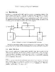
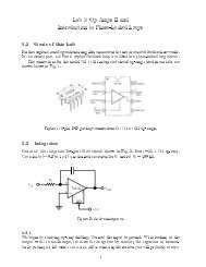
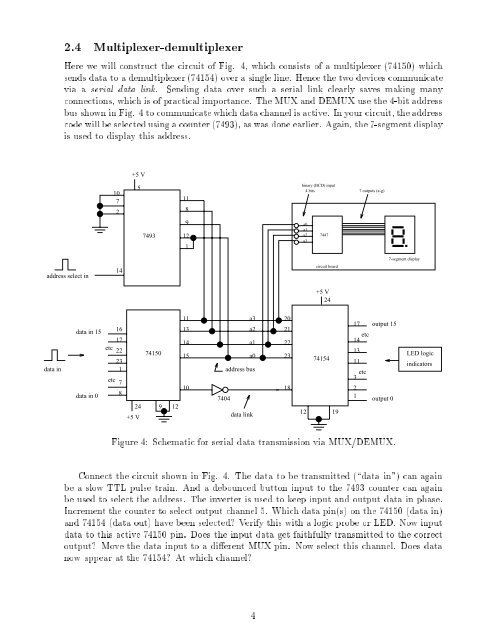
2.4 Multiplexer-demultiplexerHere we will construct the circuit of Fig. 4, which consists of a multiplexer (74150) whichsends data to a demultiplexer (74154) over a single line. Hence the two devices communicatevia a serial data link. Sending data over such a serial link clearly saves making manyconnections, which is of practical importance. The MUX <strong>and</strong> DEMUX use the 4-bit addressbus shown in Fig. 4 to communicate whichdatachannel is active. In your circuit, the addresscode will be selected using a counter (7493), as was done earlier. Again, the 7-segment displayis used to display this address.+5 V10725118binary (BCD) input4 bits 7 outputs (a-g)74939121a0a1a2a374477-segment displayaddress select in14circuit board+5 V24data indata in 15data in 01617etc22231etc787415024 9 12+5 V1113141510a3a2a1a0address bus7404data link20212223187415412 1917 output 1514 etc13113 etc21output 0LED logicindicatorsFigure 4: Schematic for serial data transmission via MUX/DEMUX.Connect the circuit shown in Fig. 4. The data to be transmitted (\data in") can againbe a slow TTL pulse train. And a debounced button input to the 7493 counter can againbe used to select the address. The inverter is used to keep input <strong>and</strong> output data in phase.Increment the counter to select output channel 5. Which data pin(s) on the 74150 (data in)<strong>and</strong> 74154 (data out) have been selected? Verify this with a logic probe or LED. Now inputdata to this active 74150 pin. Does the input data get faithfully transmitted to the correctoutput? Move the data input to a dierent MUX pin. Now select this channel. Does datanow appear at the 74154? At which channel?4