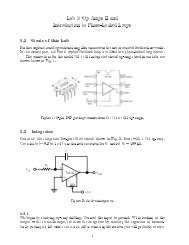
Lab 2: Decoding, Multiplexing, and Sequencing 2.1 Decoder
Lab 2: Decoding, Multiplexing, and Sequencing 2.1 Decoder
Lab 2: Decoding, Multiplexing, and Sequencing 2.1 Decoder

You also want an ePaper? Increase the reach of your titles
YUMPU automatically turns print PDFs into web optimized ePapers that Google loves.
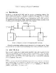
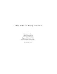
2.3 Demultiplexerdata in12logicswitchesa2a1a0131415744211 output 91097LED logic3 etc output 0indicators+5 Vgnd16821Figure 3: Demultiplexer circuit schematic.Consider Fig. 3. While a decoder is often used as part of a multiplexer, in this con-guration the 7442 decoder becomes a 1 ! 8demultiplexer. Recall that a demultiplexer(\DEMUX") routes data on a single input to one of several possible output locations, asselected by an input address. In this case, the three least-signicant address bit inputs areused to select the output location, while the most-signicant bit (MSB) at pin 12 becomesthe data input. The data gets routed to output lines 0 to 7. To see how thisworks, examinethe 7442 truth table shown below inTable 2. It uses \negative true" logic for the outputs,but in the table (from the manufacturer) 0 =LOW <strong>and</strong> 1 =HIGH. We see that when the MSB(\D") is LOW, the output selected by the other three bits is LOW, <strong>and</strong> vice versa.Construct the circuit shown in Fig. 3. Use a slow ( 1 Hz) TTL square wave as the datainput. Select an output channel using logic switches. Connect the outputs 0{7 to the 8 logicLEDs on your prototype board. Does the input data appear at the selected output? Whatappears at the other channels? Repeat with a dierent channel.3