SL811HS Embedded USB Host/Slave Controller
SL811HS Embedded USB Host/Slave Controller
SL811HS Embedded USB Host/Slave Controller

You also want an ePaper? Increase the reach of your titles
YUMPU automatically turns print PDFs into web optimized ePapers that Google loves.
<strong>SL811HS</strong><br />
<strong>SL811HS</strong> <strong>Embedded</strong> <strong>USB</strong> <strong>Host</strong>/<strong>Slave</strong> <strong>Controller</strong><br />
Features<br />
• First <strong>USB</strong> <strong>Host</strong>/<strong>Slave</strong> controller for embedded systems in<br />
the market with a standard microprocessor bus interface<br />
• Supports both full speed (12 Mbps) and low speed (1.5<br />
Mbps) <strong>USB</strong> transfer in both master and slave modes<br />
• Conforms to <strong>USB</strong> Specification 1.1 for full- and low speed<br />
• Operates as a single <strong>USB</strong> host or slave under software<br />
control<br />
• Automatic detection of either low- or full speed devices<br />
• 8-bit bidirectional data, port I/O (DMA supported in slave<br />
mode)<br />
• On-chip SIE and <strong>USB</strong> transceivers<br />
• On-chip single root HUB support<br />
• 256-byte internal SRAM buffer<br />
• Ping-pong buffers for improved performance<br />
• Operates from 12 or 48 MHz crystal or oscillator (built-in<br />
DPLL)<br />
• 5V-tolerant interface<br />
• Suspend/resume, wake up, and low-power modes are<br />
supported<br />
• Auto-generation of SOF and CRC5/16<br />
• Auto-address increment mode, saves memory<br />
READ/WRITE cycles<br />
• Development kit including source code drivers is available<br />
• 3.3V power source, 0.35 micron CMOS technology<br />
• Available in both a 28-pin PLCC package and a 48-pin<br />
TQFP package<br />
Introduction<br />
The <strong>SL811HS</strong> is an <strong>Embedded</strong> <strong>USB</strong> <strong>Host</strong>/<strong>Slave</strong> <strong>Controller</strong><br />
capable of communicating in either full speed or low speed.<br />
The <strong>SL811HS</strong> interfaces to devices such as microprocessors,<br />
microcontrollers, DSPs, or directly to a variety of buses such<br />
as ISA, PCMCIA, and others. The <strong>SL811HS</strong> <strong>USB</strong> <strong>Host</strong><br />
<strong>Controller</strong> conforms to <strong>USB</strong> Specification 1.1.<br />
The <strong>SL811HS</strong> incorporates <strong>USB</strong> Serial Interface functionality<br />
along with internal full or low speed transceivers. The<br />
<strong>SL811HS</strong> supports and operates in <strong>USB</strong> full speed mode at 12<br />
Mbps, or in low speed mode at 1.5 Mbps. When in host mode,<br />
the <strong>SL811HS</strong> is the master and controls the <strong>USB</strong> bus and the<br />
devices that are connected to it. In peripheral mode, otherwise<br />
known as a slave device, the <strong>SL811HS</strong> operates as a variety<br />
of full- or low speed devices.<br />
The <strong>SL811HS</strong> data port and microprocessor interface provide<br />
an 8-bit data path I/O or DMA bidirectional, with interrupt<br />
support to allow easy interface to standard microprocessors or<br />
microcontrollers such as Motorola or Intel CPUs and many<br />
others. The <strong>SL811HS</strong> has 256-bytes of internal RAM which is<br />
used for control registers and data buffer.<br />
The available package types offered are a 28-pin PLCC<br />
(<strong>SL811HS</strong>) and the lead-free packages are a 28-pin<br />
(<strong>SL811HS</strong>-JCT) and a 48-pin (<strong>SL811HS</strong>T-AXC) package. All<br />
packages operate at 3.3 VDC. The I/O interface logic is<br />
5V-tolerant.<br />
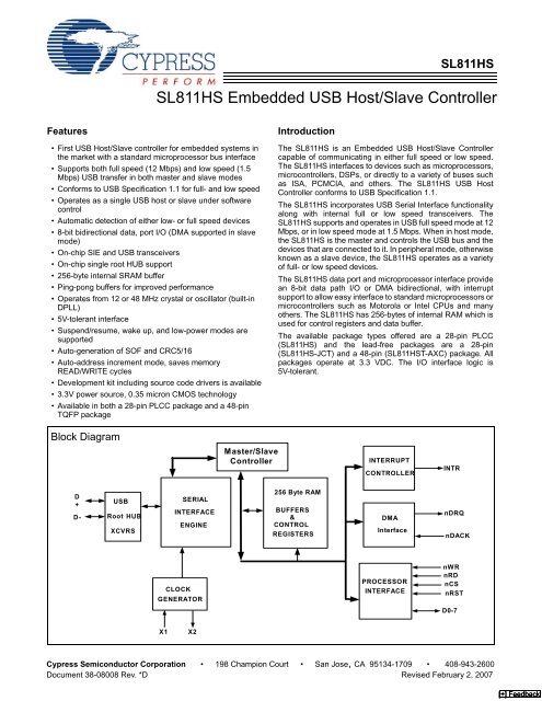
Block Diagram<br />
Master/<strong>Slave</strong><br />
<strong>Controller</strong><br />
INTERRUPT<br />
CONTROLLER<br />
INTR<br />
D<br />
+<br />
D-<br />
<strong>USB</strong><br />
Root HUB<br />
XCVRS<br />
SERIAL<br />
INTERFACE<br />
ENGINE<br />
256 Byte RAM<br />
BUFFERS<br />
&<br />
CONTROL<br />
REGISTERS<br />
DMA<br />
Interface<br />
nDRQ<br />
nDACK<br />
CLOCK<br />
GENERATOR<br />
PROCESSOR<br />
INTERFACE<br />
nWR<br />
nRD<br />
nCS<br />
nRST<br />
D0-7<br />
X1<br />
X2<br />
Cypress Semiconductor Corporation • 198 Champion Court • San Jose, CA 95134-1709 • 408-943-2600<br />
Document 38-08008 Rev. *D Revised February 2, 2007<br />
[+] Feedback
<strong>SL811HS</strong><br />
Data Port, Microprocessor Interface<br />
The <strong>SL811HS</strong> microprocessor interface provides an 8-bit<br />
bidirectional data path along with appropriate control lines to<br />
interface to external processors or controllers. Programmed<br />
I/O or memory mapped I/O designs are supported through the<br />
8-bit interface, chip select, read and write input strobes, and a<br />
single address line, A0.<br />
Access to memory and control register space is a simple two<br />
step process, requiring an address Write with A0 = ’0’, followed<br />
by a register/memory Read or Write cycle with address line A0<br />
= ’1’.<br />
In addition, a DMA bidirectional interface in slave mode is<br />
available with handshake signals such as nDRQ, nDACK,<br />
nWR, nRD, nCS and INTRQ.<br />
The <strong>SL811HS</strong> WRITE or READ operation terminates when<br />
either nWR or nCS goes inactive. For devices interfacing to<br />
the <strong>SL811HS</strong> that deactivate the Chip Select nCS before the<br />
Write nWR, the data hold timing must be measured from the<br />
nCS and will be the same value as specified. Therefore, both<br />
Intel ® - and Motorola-type CPUs work easily with the <strong>SL811HS</strong><br />
without any external glue logic requirements.<br />
DMA <strong>Controller</strong> (slave mode only)<br />
In applications that require transfers of large amounts of data<br />
such as scanner interfaces, the <strong>SL811HS</strong> provides a DMA interface.<br />
This interface supports DMA READ or WRITE transfers<br />
to the <strong>SL811HS</strong> internal RAM buffer, it is done through the<br />
microprocessor data bus via two control lines (nDRQ - Data<br />
Request and nDACK - Data Acknowledge), along with the<br />
nWR line and controls the data flow into the <strong>SL811HS</strong>. The<br />
<strong>SL811HS</strong> has a count register that allows selection of programmable<br />
block sizes for DMA transfer. The control signals,<br />
both nDRQ and nDACK, are designed for compatibility with<br />
standard DMA interfaces.<br />
Interrupt <strong>Controller</strong><br />
The <strong>SL811HS</strong> interrupt controller provides a single output<br />
signal (INTRQ) that is activated by a number of programmable<br />
events that may occur as result of <strong>USB</strong> activity. Control and<br />
status registers are provided to allow the user to select single<br />
or multiple events, which generate an interrupt (assert INTRQ)<br />
and let the user view interrupt status. The interrupts are<br />
cleared by writing to the Interrupt Status Register.<br />
Buffer Memory<br />
The <strong>SL811HS</strong> contains 256 bytes of internal memory used for<br />
<strong>USB</strong> data buffers, control registers, and status registers. When<br />
in master mode (host mode), the memory is defined where the<br />
first 16 bytes are registers and the remaining 240 bytes are<br />
used for <strong>USB</strong> data buffers. When in slave mode (peripheral<br />
mode), the first 64 bytes are used for the four endpoint control<br />
and status registers along with the various other registers. This<br />
leaves 192 bytes of endpoint buffer space for <strong>USB</strong> data<br />
transfers.<br />
Access to the registers and data memory is through the 8-bit<br />
external microprocessor data bus, in either indexed or direct<br />
addressing. Indexed mode uses the Auto Address Increment<br />
mode described in Auto Address Increment Mode, where<br />
direct addressing is used to READ/WRITE to an individual<br />
address.<br />
<strong>USB</strong> transactions are automatically routed to the memory<br />
buffer that is configured for that transfer. Control registers are<br />
provided so that pointers and block sizes in buffer memory are<br />
determined and allocated.<br />
16 bytes 0x00 – 0x0F Control<br />
0x00 – 0x39<br />
and status registers 64 bytes Control/status registers<br />
and endpoint<br />
control/status registers<br />
240 bytes<br />
0x10 – 0xFF<br />
<strong>USB</strong> data buffer<br />
<strong>Host</strong> Mode Memory Map<br />
Figure 1. Memory Map<br />
192 bytes<br />
0x40 – 0xFF<br />
<strong>USB</strong> data buffer<br />
Peripheral Mode Memory Map<br />
Auto Address Increment Mode<br />
The <strong>SL811HS</strong> supports auto increment mode to reduce READ<br />
and WRITE memory cycles. In this mode, the microcontroller<br />
needs to set up the address only once. Whenever any subsequent<br />
DATA is accessed, the internal address counter advances<br />
to the next address location.<br />
Auto Address Increment Example. To fill the data buffer<br />
that is configured for address 10h, follow these steps:<br />
1. Write 10h to <strong>SL811HS</strong> with A0 LOW. This sets the memory<br />
address that is used for the next operation.<br />
2. Write the first data byte into address 10h by doing a write<br />
operation with A0 HIGH. An example is a Get Descriptor;<br />
the first byte that is sent to the device is 80h<br />
(bmRequestType) so you would write 80h to address 10h.<br />
3. Now the internal RAM address pointer is set to 11h. So, by<br />
doing another write with A0 HIGH, RAM address location<br />
11h is written with the data. Continuing with the Get<br />
Descriptor example, a 06h is written to address 11h for the<br />
bRequest value.<br />
4. Repeat Step 3 until all the required bytes are written as<br />
necessary for a transfer. If auto-increment is not used, you<br />
write the address value each time before writing the data<br />
as shown in Step 1.<br />
The advantage of auto address increment mode is that it<br />
reduces the number of required <strong>SL811HS</strong> memory<br />
READ/WRITE cycles to move data to/from the device. For<br />
example, transferring 64 bytes of data to/from <strong>SL811HS</strong>, using<br />
auto increment mode, reduces the number of cycles to 1<br />
address WRITE and 64 READ/WRITE data cycles, compared<br />
to 64 address writes and 64 data cycles for random access.<br />
Document 38-08008 Rev. *D Page 2 of 32<br />
[+] Feedback
<strong>SL811HS</strong><br />
PLL Clock Generator<br />
Either a 12 MHz or a 48 MHz external crystal is used with the<br />
<strong>SL811HS</strong> [1] . Two pins, X1 and X2, are provided to connect a<br />
low cost crystal circuit to the device as shown in Figure 2 and<br />
Figure 3. Use an external clock source if available in the application<br />
instead of the crystal circuit by connecting the source<br />
directly to the X1 input pin. When a clock is used, the X2 pin<br />
is not connected.<br />
When the CM pin is tied to a logic 0, the internal PLL is<br />
bypassed so the clock source must meet the timing requirements<br />
specified by the <strong>USB</strong> specification.<br />
Figure 2. Full Speed 48 MHz Crystal Circuit<br />
Cin<br />
22 pF<br />
X1<br />
Cbk<br />
0.01 μF<br />
Lin<br />
2.2 μH<br />
Rf<br />
1M<br />
X1<br />
48 MHz, series, 20-pF load<br />
X2<br />
Rs<br />
100<br />
Cout<br />
22 pF<br />
Typical Crystal Requirements<br />
The following are examples of ‘typical requirements.’ Note that<br />
these specifications are generally found as standard crystal<br />
values and are less expensive than custom values. If crystals<br />
are used in series circuits, load capacitance is not applicable.<br />
Load capacitance of parallel circuits is a requirement. 48 MHz<br />
third overtone crystals require the Cin/Lin filter to guarantee 48<br />
MHz operation.<br />
12 MHz Crystals:<br />
Frequency Tolerance:<br />
±100 ppm or better<br />
Operating Temperature Range: 0°C to 70°C<br />
Frequency:<br />
Frequency Drift over Temperature:<br />
ESR (Series Resistance):<br />
Load Capacitance:<br />
Shunt Capacitance:<br />
Drive Level:<br />
Operating Mode:<br />
48 MHz Crystals:<br />
Frequency Tolerance:<br />
12 MHz<br />
± 50 ppm<br />
60Ω<br />
10 pF min.<br />
7 pF max.<br />
0.1–0.5 mW<br />
fundamental<br />
±100 ppm or better<br />
Operating Temperature Range: 0°C to 70°C<br />
Frequency:<br />
Frequency Drift over Temperature:<br />
ESR (Series Resistance):<br />
Load Capacitance:<br />
Shunt Capacitance:<br />
Drive Level:<br />
Operating Mode:<br />
48 MHz<br />
± 50 ppm<br />
40 Ω<br />
10 pF min.<br />
7 pF max.<br />
0.1–0.5 mW<br />
third overtone<br />
X1<br />
Figure 3. Optional 12 MHz Crystal Circuit<br />
Cin<br />
22 pF<br />
Rf<br />
1M<br />
X1<br />
12 MHz , series, 20-pF load<br />
Cout<br />
22 pF<br />
<strong>USB</strong> Transceiver<br />
The <strong>SL811HS</strong> has a built in transceiver that meets <strong>USB</strong> Specification<br />
1.1. The transceiver is capable of transmitting and<br />
receiving serial data at <strong>USB</strong> full speed (12 Mbits) and low<br />
speed (1.5 Mbits). The driver portion of the transceiver is differential<br />
while the receiver section is comprised of a differential<br />
receiver and two single-ended receivers. Internally, the transceiver<br />
interfaces to the Serial Interface Engine (SIE) logic.<br />
Externally, the transceiver connects to the physical layer of the<br />
<strong>USB</strong>.<br />
<strong>SL811HS</strong> Registers<br />
Operation and control of the <strong>SL811HS</strong> is managed through<br />
internal registers. When operating in Master/<strong>Host</strong> mode, the<br />
first 16 address locations are defined as register space. In<br />
<strong>Slave</strong>/Peripheral mode, the first 64 bytes are defined as<br />
register space. The register definitions vary greatly between<br />
each mode of operation and are defined separately in this<br />
document (section “<strong>SL811HS</strong> Master (<strong>Host</strong>) Mode Registers”<br />
on page 4 describes <strong>Host</strong> register definitions, while section<br />
Note<br />
1. CM (Clock Multiply) pin of the <strong>SL811HS</strong> must be tied to GND when 48 MHz crystal circuit or 48 MHz clock source is used.<br />
X2<br />
Rs<br />
100<br />
Document 38-08008 Rev. *D Page 3 of 32<br />
[+] Feedback
<strong>SL811HS</strong><br />
“<strong>SL811HS</strong> <strong>Slave</strong> Mode Registers” on page 12 describes <strong>Slave</strong><br />
register definitions). Access to the registers are through the<br />
microprocessor interface similar to normal RAM accesses<br />
(see “Bus Interface Timing Requirements” on page 26) and<br />
provide control and status information for <strong>USB</strong> transactions.<br />
Any write to control register 0FH enables the <strong>SL811HS</strong> full<br />
features bit. This is an internal bit of the <strong>SL811HS</strong> that enables<br />
additional features.<br />
Table 1 shows the memory map and register mapping of the<br />
<strong>SL811HS</strong> in master/host mode.<br />
<strong>SL811HS</strong> Master (<strong>Host</strong>) Mode Registers<br />
Table 1.<br />
<strong>SL811HS</strong> Master (<strong>Host</strong>) Register Summary<br />
Register Name<br />
<strong>SL811HS</strong><br />
<strong>USB</strong>-A <strong>Host</strong> Control Register<br />
<strong>USB</strong>-A <strong>Host</strong> Base Address<br />
<strong>USB</strong>-A <strong>Host</strong> Base Length<br />
<strong>USB</strong>-A <strong>Host</strong> PID, Device Endpoint<br />
(Write)/<strong>USB</strong> Status (Read)<br />
<strong>USB</strong>-A <strong>Host</strong> Device Address (Write)/Transfer<br />
Count (Read)<br />
Control Register 1<br />
Interrupt Enable Register<br />
Reserved Register<br />
<strong>USB</strong>-B <strong>Host</strong> Control Register<br />
<strong>USB</strong>-B <strong>Host</strong> Base Address<br />
<strong>USB</strong>-B <strong>Host</strong> Base Length<br />
<strong>USB</strong>-B <strong>Host</strong> PID, Device Endpoint<br />
(Write)/<strong>USB</strong> Status (Read)<br />
<strong>USB</strong>-B <strong>Host</strong> Device Address (Write)/Transfer<br />
Count (Read)<br />
Status Register<br />
SOF Counter LOW (Write)/HW Revision Register<br />
(Read)<br />
SOF Counter HIGH and Control Register 2<br />
Memory Buffer<br />
<strong>SL811HS</strong><br />
(hex) Address<br />
00h<br />
01h<br />
02h<br />
03h<br />
04h<br />
05h<br />
06h<br />
Reserved<br />
08h<br />
09h<br />
0Ah<br />
0Bh<br />
0Ch<br />
0Dh<br />
0Eh<br />
0Fh<br />
10H-FFh<br />
The registers in the <strong>SL811HS</strong> are divided into two major<br />
groups. The first group is referred to as <strong>USB</strong> Control registers.<br />
These registers enable and provide status for control of <strong>USB</strong><br />
transactions and data flow. The second group of registers<br />
provides control and status for all other operations.<br />
All other register’s power up and reset in an unknown state and<br />
firmware for initialization.<br />
<strong>USB</strong> Control Registers<br />
Communication and data flow on the <strong>USB</strong> bus uses the<br />
<strong>SL811HS</strong>’ <strong>USB</strong> A-B Control registers. The <strong>SL811HS</strong> communicates<br />
with any <strong>USB</strong> Device function and any specific<br />
endpoint via the <strong>USB</strong>-A or <strong>USB</strong>-B register sets.<br />
The <strong>USB</strong> A-B <strong>Host</strong> Control registers are used in an overlapped<br />
configuration to manage traffic on the <strong>USB</strong> bus. The <strong>USB</strong> <strong>Host</strong><br />
Control register also provides a means to interrupt an external<br />
CPU or microcontroller when one of the <strong>USB</strong> protocol transactions<br />
is completed. Table 1 and Table 2 show the two sets of<br />
<strong>USB</strong> <strong>Host</strong> Control registers, the ’A’ set and ’B’ set. The two<br />
register sets allow for overlapping operation. When one set of<br />
parameters is being set up, the other is transferring. On<br />
completion of a transfer to an endpoint, the next operation is<br />
controlled by the other register set.<br />
Note The <strong>USB</strong>-B register set is used only when <strong>SL811HS</strong><br />
mode is enabled by initializing register 0FH.<br />
The <strong>SL811HS</strong> <strong>USB</strong> <strong>Host</strong> Control has two groups of five<br />
registers each which map in the <strong>SL811HS</strong> memory space.<br />
These registers are defined in the following tables.<br />
<strong>SL811HS</strong> <strong>Host</strong> Control Registers.<br />
Table 2. <strong>SL811HS</strong> <strong>Host</strong> Control Registers<br />
Register Name SL811H<br />
<strong>USB</strong>-A <strong>Host</strong> Control Register<br />
<strong>USB</strong>-A <strong>Host</strong> Base Address<br />
<strong>USB</strong>-A <strong>Host</strong> Base Length<br />
<strong>USB</strong>-A <strong>Host</strong> PID, Device Endpoint<br />
(Write)/<strong>USB</strong> Status (Read)<br />
<strong>USB</strong>-A <strong>Host</strong> Device Address (Write)/Transfer<br />
Count (Read)<br />
<strong>USB</strong>-B <strong>Host</strong> Control Register<br />
<strong>USB</strong>-B <strong>Host</strong> Base Address<br />
<strong>USB</strong>-B <strong>Host</strong> Base Length<br />
<strong>USB</strong>-B <strong>Host</strong> PID, Device Endpoint<br />
(Write)/<strong>USB</strong> Status (Read)<br />
<strong>USB</strong>-B <strong>Host</strong> Device Address (Write)/Transfer<br />
Count (Read)<br />
<strong>SL811HS</strong><br />
(hex) Address<br />
00h<br />
01h<br />
02h<br />
03h<br />
04h<br />
08h<br />
09h<br />
0Ah<br />
0Bh<br />
0Ch<br />
Register Values on Power Up and Reset<br />
The following registers initialize to zero on power up and reset:<br />
• <strong>USB</strong>-A/<strong>USB</strong>-B <strong>Host</strong> Control Register [00H, 08H] bit 0 only<br />
• Control Register 1 [05H]<br />
• <strong>USB</strong> Address Register [07H]<br />
• Current Data Set/Hardware Revision/SOF Counter LOW<br />
Register [0EH]<br />
Document 38-08008 Rev. *D Page 4 of 32<br />
[+] Feedback
<strong>SL811HS</strong><br />
<strong>USB</strong>-A/<strong>USB</strong>-B <strong>Host</strong> Control Registers [Address = 00h, 08h] .<br />
Table 3. <strong>USB</strong>-A/<strong>USB</strong>-B <strong>Host</strong> Control Register Definition [Address 00h, 08h]<br />
Bit 7 Bit 6 Bit 5 Bit 4 Bit 3 Bit 2 Bit 1 Bit 0<br />
Preamble Data Toggle Bit SyncSOF ISO Reserved Direction Enable Arm<br />
Bit Position Bit Name Function<br />
7 Preamble If bit = ’1’ a preamble token is transmitted before transfer of low speed packet. If bit = ’0’,<br />
preamble generation is disabled.<br />
• The <strong>SL811HS</strong> automatically generates preamble packets when bit 7 is set. This bit is only<br />
used to send packets to a low speed device through a hub. To communicate to a full<br />
speed device, this bit is set to ‘0’. For example, when <strong>SL811HS</strong> communicates to a low<br />
speed device via the HUB:<br />
— Set <strong>SL811HS</strong> SIE to operate at full speed, i.e., bit 5 of register 05h (Control Register 1)<br />
= ’0’.<br />
— Set bit 6 of register 0Fh (Control Register 2) = ’0’. Set correct polarity of DATA+ and<br />
DATA– state for full speed.<br />
— Set bit 7, Preamble bit, = ’1’ in the <strong>Host</strong> Control register.<br />
• When <strong>SL811HS</strong> communicates directly to a low speed device:<br />
— Set bit 5 of register 05h (Control Register 1) = ’1’.<br />
— Set bit 6 of register 0Fh (Control Register 2) = ’1’, DATA+ and DATA– polarity for low<br />
speed.<br />
— The state of bit 7 is ignored in this mode.<br />
6 Data Toggle Bit ’0’ if DATA0, ’1’ if DATA1 (only used for OUT tokens in host mode).<br />
5 SyncSOF ’1’ = Synchronize with the SOF transfer when operating in FS only.<br />
The <strong>SL811HS</strong> uses bit 5 to enable transfer of a data packet after a SOF packet is transmitted.<br />
When bit 5 = ‘1’, the next enabled packet is sent after next SOF. If bit 5 = ‘0’ the next packet<br />
is sent immediately if the SIE is free. If operating in low speed, do not set this bit.<br />
4 ISO When set to ’1’, this bit allows Isochronous mode for this packet.<br />
3 Reserved Bit 3 is reserved for future use.<br />
2 Direction When equal to ’1’ transmit (OUT). When equal to ’0’ receive (IN).<br />
1 Enable If Enable = ’1’, this bit allows transfers to occur. If Enable = ’0’, <strong>USB</strong> transactions are ignored.<br />
The Enable bit is used in conjunction with the Arm bit (bit 0 of this register) for <strong>USB</strong> transfers.<br />
0 Arm Allows enabled transfers when Arm = ’1’. Cleared to ’0’ when transfer is complete (when<br />
Done Interrupt is asserted).<br />
Once the other <strong>SL811HS</strong> Control registers are configured (registers 01h-04h or 09h-0Ch) the <strong>Host</strong> Control register is programmed<br />
to initiate the <strong>USB</strong> transfer. This register initiates the transfer when the Enable and Arm bit are set as described above.<br />
<strong>USB</strong>-A/<strong>USB</strong>-B <strong>Host</strong> Base Address [Address = 01h, 09h] .<br />
Table 4. <strong>USB</strong>-A/<strong>USB</strong>-B <strong>Host</strong> Base Address Definition [Address 01h, 09h]<br />
Bit 7 Bit 6 Bit 5 Bit 4 Bit 3 Bit 2 Bit 1 Bit 0<br />
HBADD7 HBADD6 HBADD5 HBADD4 HBADD3 HBADD2 HBADD1 HBADD0<br />
The <strong>USB</strong>-A/B Base Address is a pointer to the <strong>SL811HS</strong> memory buffer location for <strong>USB</strong> reads and writes. When transferring<br />
data OUT (<strong>Host</strong> to Device), the <strong>USB</strong>-A and <strong>USB</strong>-B <strong>Host</strong> Base Address registers can be set up before setting ARM on the <strong>USB</strong>-A<br />
or <strong>USB</strong>-B <strong>Host</strong> Control register. When using a double buffer scheme, the <strong>Host</strong> Base Address could be set up with the first buffer<br />
used for DATA0 data and the other for DATA1 data.<br />
Document 38-08008 Rev. *D Page 5 of 32<br />
[+] Feedback
<strong>SL811HS</strong><br />
<strong>USB</strong>-A/<strong>USB</strong>-B <strong>Host</strong> Base Length [Address = 02h, 0Ah].<br />
Table 5.<br />
<strong>USB</strong>-A / <strong>USB</strong>-B <strong>Host</strong> Base Length Definition [Address 02h, 0Ah]<br />
Bit 7 Bit 6 Bit 5 Bit 4 Bit 3 Bit 2 Bit 1 Bit 0<br />
HBL7 HBL6 HBL5 HBL4 HBL3 HBL2 HBL1 HBL0<br />
The <strong>USB</strong> A/B <strong>Host</strong> Base Length register contains the maximum packet size transferred between the <strong>SL811HS</strong> and a slave <strong>USB</strong><br />
peripheral. Essentially, this designates the largest packet size that is transferred by the <strong>SL811HS</strong>. Base Length designates the<br />
size of data packet sent or received. For example, in full speed BULK mode, the maximum packet length is 64 bytes. In ISO<br />
mode, the maximum packet length is 1023 bytes since the <strong>SL811HS</strong> only has an 8-bit length; the maximum packet size for the<br />
ISO mode using the <strong>SL811HS</strong> is 255 – 16 bytes (register space). When the <strong>Host</strong> Base length register is set to zero, a Zero-Length<br />
packet is transmitted.<br />
<strong>USB</strong>-A/<strong>USB</strong>-B <strong>USB</strong> Packet Status (Read) and <strong>Host</strong> PID, Device Endpoint (Write) [Address = 03h, 0Bh]. This register has<br />
two modes dependent on whether it is read or written. When read, this register provides packet status and contains information<br />
relative to the last packet that has been received or transmitted. This register is not valid for reading until after the Done interrupt<br />
occurs, which causes the register to update.<br />
Table 6.<br />
<strong>USB</strong>-A/<strong>USB</strong>-B <strong>USB</strong> Packet Status Register Definition when READ [Address 03h, 0Bh]<br />
Bit 7 Bit 6 Bit 5 Bit 4 Bit 3 Bit 2 Bit 1 Bit 0<br />
STALL NAK Overflow Setup Sequence Time-out Error ACK<br />
Bit Position Bit Name Function<br />
7 STALL <strong>Slave</strong> device returned a STALL.<br />
6 NAK <strong>Slave</strong> device returned a NAK.<br />
5 Overflow Overflow condition - maximum length exceeded during receives. For underflow, see<br />
<strong>USB</strong>-A/<strong>USB</strong>-B <strong>Host</strong> Transfer Count Register (Read), <strong>USB</strong> Address (Write) [Address = 04h,<br />
0Ch] on page 7.<br />
4 Setup This bit is not applicable for <strong>Host</strong> operation since a SETUP packet is generated by the host.<br />
3 Sequence Sequence bit. ’0’ if DATA0, ’1’ if DATA1.<br />
2 Time-out Timeout occurred. A timeout is defined as 18-bit times without a device response (in full<br />
speed).<br />
1 Error Error detected in transmission. This includes CRC5, CRC16, and PID errors.<br />
0 ACK Transmission Acknowledge.<br />
When written, this register provides the PID and Endpoint information to the <strong>USB</strong> SIE engine used in the next transaction. All 16<br />
Endpoints can be addressed by the <strong>SL811HS</strong>.<br />
Table 7.<br />
<strong>USB</strong>-A / <strong>USB</strong>-B <strong>Host</strong> PID and Device Endpoint Register when WRITTEN [Address 03h, 0Bh]<br />
Bit 7 Bit 6 Bit 5 Bit 4 Bit 3 Bit 2 Bit 1 Bit 0<br />
PID3 PID2 PID1 PID0 EP3 EP2 EP1 EP0<br />
PID[3:0]: 4-bit PID Field (See Table Below), EP[3:0]: 4-bit Endpoint Value in Binary.<br />
PID TYPE<br />
SETUP<br />
IN<br />
OUT<br />
SOF<br />
PREAMBLE<br />
NAK<br />
STALL<br />
DATA0<br />
DATA1<br />
D7-D4<br />
1101 (D Hex)<br />
1001 (9 Hex)<br />
0001 (1 Hex)<br />
0101 (5 Hex)<br />
1100 (C Hex)<br />
1010 (A Hex)<br />
1110 (E Hex)<br />
0011 (3 Hex)<br />
1011 (B Hex)<br />
Document 38-08008 Rev. *D Page 6 of 32<br />
[+] Feedback
<strong>SL811HS</strong><br />
<strong>USB</strong>-A/<strong>USB</strong>-B <strong>Host</strong> Transfer Count Register (Read), <strong>USB</strong> Address (Write) [Address = 04h, 0Ch]. This register has two<br />
different functions depending on whether it is read or written. When read, this register contains the number of bytes remaining<br />
(from <strong>Host</strong> Base Length value) after a packet is transferred. For example, if the Base Length register is set to 0x040 and an IN<br />
Token was sent to the peripheral device. If, after the transfer is complete, the value of the <strong>Host</strong> Transfer Count is 0x10, the number<br />
of bytes actually transferred is 0x30. This is considered as an underflow indication.<br />
Table 8.<br />
<strong>USB</strong>-A / <strong>USB</strong>-B <strong>Host</strong> Transfer Count Register when READ [Address 04h, 0Ch]<br />
Bit 7 Bit 6 Bit 5 Bit 4 Bit 3 Bit 2 Bit 1 Bit 0<br />
HTC7 HTC6 HTC5 HTC4 HTC3 HTC2 HTC1 HTC0<br />
When written, this register contains the <strong>USB</strong> Device Address with which the <strong>Host</strong> communicates.<br />
Table 9. <strong>USB</strong>-A / <strong>USB</strong>-B <strong>USB</strong> Address when WRITTEN [Address 04h, 0Ch]<br />
Bit 7 Bit 6 Bit 5 Bit 4 Bit3 Bit 2 Bit 1 Bit 0<br />
0 DA6 DA5 DA4 DA3 DA2 DA1 DA0<br />
DA6-DA0<br />
DA7<br />
Device address, up to 127 devices can be addressed.<br />
Reserved bit must be set to zero.<br />
<strong>SL811HS</strong> Control Registers<br />
The next set of registers are the Control registers and control more of the operation of the chip instead of <strong>USB</strong> packet type of<br />
transfers. Table 10 is a summary of the control registers.<br />
Table 10. <strong>SL811HS</strong> Control Registers Summary<br />
Register Name SL811H<br />
Control Register 1<br />
Interrupt Enable Register<br />
Reserved Register<br />
Status Register<br />
SOF Counter LOW (Write)/HW Revision Register (Read)<br />
SOF Counter HIGH and Control Register 2<br />
Memory Buffer<br />
<strong>SL811HS</strong> (hex) Address<br />
05h<br />
06h<br />
07h<br />
0Dh<br />
0Eh<br />
0Fh<br />
10h-FFh<br />
Document 38-08008 Rev. *D Page 7 of 32<br />
[+] Feedback
<strong>SL811HS</strong><br />
Control Register 1 [Address = 05h]. The Control Register 1 enables/disables <strong>USB</strong> transfer operation with control bits defined<br />
as follows.<br />
Table 11. Control Register 1 [Address 05h]<br />
Bit 7 Bit 6 Bit 5 Bit 4 Bit 3 Bit 2 Bit 1 Bit 0<br />
Reserved Suspend <strong>USB</strong> Speed J-K state force <strong>USB</strong> Engine Reserved Reserved SOF ena/dis<br />
Reset<br />
Bit Position Bit Name Function<br />
7 Reserved ‘0’<br />
6 Suspend ’1’ = enable, ’0’ = disable.<br />
5 <strong>USB</strong> Speed ’0’ setup for full speed, ’1’ setup low speed.<br />
4 J-K state force See Table 12.<br />
3 <strong>USB</strong> Engine Reset <strong>USB</strong> Engine reset = ’1’. Normal set ’0’.<br />
When a device is detected, the first thing that to do is to send it a <strong>USB</strong> Reset to force it into<br />
its default address of zero. The <strong>USB</strong> 2.0 specification states that for a root hub a device<br />
must be reset for a minimum of 50 mS.<br />
2 Reserved Some existing firmware examples set bit 2, but it is not necessary.<br />
1 Reserved ‘0’<br />
0 SOF ena/dis ’1’ = enable auto Hardware SOF generation; ’0’ = disable.<br />
In the <strong>SL811HS</strong>, bit 0 is used to enable hardware SOF autogeneration. The generation of<br />
SOFs continues when set to ‘0’, but SOF tokens are not output to <strong>USB</strong>.<br />
At powe -up this register is cleared to all zeros.<br />
Low-power Modes [Bit 6 Control Register, Address 05h]<br />
When bit 6 (Suspend) is set to ’1’, the power of the transmit<br />
transceiver is turned off, the internal RAM is in suspend mode,<br />
and the internal clocks are disabled.<br />
Note Any activity on the <strong>USB</strong> bus (i.e., K-State, etc.) resumes<br />
normal operation. To resume normal operation from the CPU<br />
side, a Data Write cycle (i.e., A0 set HIGH for a Data Write<br />
cycle) is done. This is a special case and not a normal direct<br />
write where the address is first written and then the data. To<br />
resume normal operation from the CPU side, you must do a<br />
Data Write cycle only.<br />
Low Speed/Full Speed Modes [Bit 5 Control Register 1,<br />
Address 05h]<br />
The <strong>SL811HS</strong> is designed to communicate with either full- or<br />
low speed devices. At power up bit 5 is LOW, i.e., for full<br />
speed. There are two cases when communicating with a low<br />
speed device. When a low speed device is connected directly<br />
to the <strong>SL811HS</strong>, bit 5 of Register 05h is set to ’1’ and bit 6 of<br />
register 0Fh, Polarity Swap, is set to ’1’ in order to change the<br />
polarity of D+ and D–. When a low speed device is connected<br />
via a HUB to <strong>SL811HS</strong>, bit 5 of Register 05h is set to ’0’ and<br />
bit 6 of register 0Fh is set to ’0’ in order to keep the polarity of<br />
D+ and D– for full speed. In addition, make sure that bit 7 of<br />
<strong>USB</strong>-A/<strong>USB</strong>-B <strong>Host</strong> Control registers [00h, 08h] is set to ’1’ for<br />
preamble generation.<br />
J-K Programming States [Bits 4 and 3 of Control Register<br />
1, Address 05h]<br />
The J-K force state control and <strong>USB</strong> Engine Reset bits are<br />
used to generate a <strong>USB</strong> reset condition. Forcing K-state is<br />
used for Peripheral device remote wake up, resume, and other<br />
modes. These two bits are set to zero on power up.<br />
Table 12. Control Register 1 Address 05h – Bits 3 and 4<br />
Bit 4 Bit 3 Function<br />
0 0 Normal operating mode<br />
0 1 Force <strong>USB</strong> Reset, D+ and D– are set LOW (SE0)<br />
1 0 Force J-State, D+ set HIGH, D– set LOW [2]<br />
1 1 Force K-State, D– set HIGH, D+ set LOW [3]<br />
<strong>USB</strong> Reset Sequence<br />
After a device is detected, write 08h to the Control register<br />
(05h) to initiate the <strong>USB</strong> reset, then wait for the <strong>USB</strong> reset time<br />
(root hub should be 50 ms) and additionally some types of<br />
devices such as a Forced J-state. Lastly, set the Control<br />
register (05h) back to 0h. After the reset is complete, the<br />
auto-SOF generation is enabled.<br />
SOF Packet Generation<br />
The <strong>SL811HS</strong> automatically computes the frame number and<br />
CRC5 by hardware. No CRC or SOF generation is required by<br />
external firmware for the <strong>SL811HS</strong>, although it can be done by<br />
sending an SOF PID in the <strong>Host</strong> PID, Device Endpoint register.<br />
To enable SOF generation, assuming host mode is configured:<br />
1. Set up the SOF interval in registers 0x0F and 0x0E.<br />
2. Enable the SOF hardware generation in this register by<br />
setting bit 0 = ‘1’.<br />
3. Set the Arm bit in the <strong>USB</strong>-A <strong>Host</strong> Control register.<br />
Notes<br />
2. Force K-State for low speed.<br />
3. Force J-State for low speed.<br />
Document 38-08008 Rev. *D Page 8 of 32<br />
[+] Feedback
<strong>SL811HS</strong><br />
Interrupt Enable Register [Address = 06h]. The <strong>SL811HS</strong><br />
provides an Interrupt Request Output, which is activated for a<br />
number of conditions. The Interrupt Enable register allows the<br />
user to select conditions that result in an interrupt that is issued<br />
to an external CPU through the INTRQ pin. A separate<br />
Interrupt Status register reflects the reason for the interrupt.<br />
Enabling or disabling these interrupts does not have an effect<br />
on whether or not the corresponding bit in the Interrupt Status<br />
register is set or cleared; it only determines if the interrupt is<br />
routed to the INTRQ pin. The Interrupt Status register is<br />
normally used in conjunction with the Interrupt Enable register<br />
and can be polled in order to determine the conditions that<br />
initiated the interrupt (See the description for the Interrupt<br />
Status Register). When a bit is set to ’1’ the corresponding<br />
interrupt is enabled. So when the enabled interrupt occurs, the<br />
INTRQ pin is asserted. The INTRQ pin is a level interrupt,<br />
meaning it is not deasserted until all enabled interrupts are<br />
cleared.<br />
Table 13. Interrupt Enable Register [Address 06h]<br />
Bit 7 Bit 6 Bit 5 Bit 4 Bit 3 Bit 2 Bit 1 Bit 0<br />
Reserved Device<br />
Detect/Resume<br />
Inserted/<br />
Removed<br />
SOF Timer Reserved Reserved <strong>USB</strong>-B<br />
DONE<br />
<strong>USB</strong>-A<br />
DONE<br />
Bit Position Bit Name Function<br />
7 Reserved ‘0’<br />
6 Device Detect/Resume Enable Device Detect/Resume Interrupt.<br />
When bit 6 of register 05h (Control Register 1) is equal to ’1’, bit 6 of this register enables<br />
the Resume Detect Interrupt. Otherwise, this bit is used to enable Device Detection<br />
status as defined in the Interrupt Status register bit definitions.<br />
5 Inserted/Removed Enable <strong>Slave</strong> Insert/Remove Detection is used to enable/disable the device<br />
inserted/removed interrupt.<br />
4 SOF Timer 1 = Enable Interrupt for SOF Timer. This is typically at 1 mS intervals, although the<br />
timing is determined by the SOF Counter high/low registers.<br />
To use this bit function, bit 0 of register 05h must be enabled and the SOF counter<br />
registers 0E hand 0Fh must be initialized.<br />
3 Reserved ‘0’<br />
2 Reserved ‘0’<br />
1 <strong>USB</strong>-B DONE <strong>USB</strong>-B Done Interrupt (see <strong>USB</strong>-A Done interrupt).<br />
0 <strong>USB</strong>-A DONE <strong>USB</strong>-A Done Interrupt. The Done interrupt is triggered by one of the events that are<br />
logged in the <strong>USB</strong> Packet Status register. The Done interrupt causes the Packet Status<br />
register to update.<br />
<strong>USB</strong> Address Register, Reserved, Address [Address = 07h]. This register is reserved for the device <strong>USB</strong> Address in <strong>Slave</strong><br />
operation. It should not be written by the user in host mode.<br />
Registers 08h-0Ch <strong>Host</strong>-B registers. Registers 08h-0Ch have the same definition as registers 00h-04h except they apply to<br />
<strong>Host</strong>-B instead of <strong>Host</strong>-A.<br />
Document 38-08008 Rev. *D Page 9 of 32<br />
[+] Feedback
<strong>SL811HS</strong><br />
Interrupt Status Register, Address [Address = 0Dh]. The Interrupt Status register is a READ/WRITE register providing<br />
interrupt status. Interrupts are cleared by writing to this register. To clear a specific interrupt, the register is written with corresponding<br />
bit set to ’1’.<br />
Table 14. Interrupt Status Register [Address 0Dh]<br />
Bit 7 Bit 6 Bit 5 Bit 4 Bit 3 Bit 2 Bit 1 Bit 0<br />
D+ Device Insert/Remove SOF timer Reserved Reserved <strong>USB</strong>-B <strong>USB</strong>-A<br />
Detect/Resume<br />
Bit Position Bit Name Function<br />
7 D+ Value of the Data+ pin.<br />
Bit 7 provides continuous <strong>USB</strong> Data+ line status. Once it is determined that a device<br />
is inserted (as described below) with bits 5 and 6, bit 7 is used to detect if the inserted<br />
device is low speed (0) or full speed (1).<br />
6 Device Detect/Resume Device Detect/Resume Interrupt.<br />
Bit 6 is shared between Device Detection status and Resume Detection interrupt.<br />
When bit-6 of register 05h is set to one, this bit is the Resume detection Interrupt bit.<br />
Otherwise, this bit is used to indicate the presence of a device, ’1’ = device ‘Not present’<br />
and ’0’ = device ‘Present.’ In this mode, check this bit along with bit 5 to determine<br />
whether a device has been inserted or removed.<br />
5 Insert/Remove Device Insert/Remove Detection.<br />
Bit 5 is provided to support <strong>USB</strong> cable insertion/removal for the <strong>SL811HS</strong> in host mode.<br />
This bit is set when a transition from SE0 to IDLE (device inserted) or from IDLE to<br />
SE0 (device removed) occurs on the bus.<br />
4 SOF timer ‘1’ = Interrupt on SOF Timer.<br />
3 Reserved ‘0’<br />
2 Reserved ‘0’<br />
1 <strong>USB</strong>-B <strong>USB</strong>-B Done Interrupt. (See description in Interrupt Enable Register [address 06h].)<br />
0 <strong>USB</strong>-A <strong>USB</strong>-A Done Interrupt. (See description in Interrupt Enable Register [address 06h].)<br />
Current Data Set Register/Hardware Revision/SOF Counter LOW [Address = 0Eh]. This register has two modes. Read<br />
from this register indicates the current <strong>SL811HS</strong> silicon revision.<br />
Table 15. Hardware Revision when Read [Address 0Eh]<br />
Bit 7 Bit 6 Bit 5 Bit 4 Bit 3 Bit 2 Bit 1 Bit 0<br />
Hardware Revision<br />
Reserved<br />
Bit Position Bit Name Function<br />
7-4 Hardware Revision <strong>SL811HS</strong> rev1.2 Read = 1H; <strong>SL811HS</strong> rev1.5 Read = 2.<br />
3-2 Reserved Read is zero.<br />
1-0 Reserved Reserved for slave.<br />
Writing to this register sets up auto generation of SOF to all connected peripherals. This counter is based on the 12 MHz clock<br />
and is not dependent on the crystal frequency. To set up a 1 ms timer interval, the software must set up both SOF counter registers<br />
to the proper values.<br />
Document 38-08008 Rev. *D Page 10 of 32<br />
[+] Feedback
<strong>SL811HS</strong><br />
Table 16. SOF Counter LOW Address when Written [Address 0Eh]<br />
Bit 7 Bit 6 Bit 5 Bit 4 Bit 3 Bit 2 Bit 1 Bit 0<br />
SOF7 SOF6 SOF5 SOF4 SOF3 SOF2 SOF1 SOF0<br />
Example: To set up SOF for 1 ms interval, SOF counter register 0Eh should be set to E0h.<br />
SOF Counter High/Control Register 2 [Address = 0Fh]. When read, this register returns the value of the SOF counter divided<br />
by 64. The software must use this register to determine the available bandwidth in the current frame before initiating any <strong>USB</strong><br />
transfer. In this way, the user is able to avoid babble conditions on the <strong>USB</strong>. For example, to determine the available bandwidth<br />
left in a frame do the following.<br />
Maximum number of clock ticks in 1 ms time frame is 12000 (1 count per 12 MHz clock period, or approximately 84 ns.) The value<br />
read back in Register 0FH is the (count × 64) × 84 ns = time remaining in current frame. <strong>USB</strong> bit time = one 12 MHz period.<br />
Value of register 0FH Available bit times left are between<br />
BBH<br />
12000 bits to 11968 (187 × 64) bits<br />
BAH<br />
11968 bits to 11904 (186 × 64) bits<br />
Note: Any write to the 0Fh register clears the internal frame counter. Write register 0Fh at least once after power up. The internal<br />
frame counter is incremented after every SOF timer tick. The internal frame counter is an 11-bit counter, which is used to track<br />
the frame number. The frame number is incremented after each timer tick. Its contents are transmitted to the slave every millisecond<br />
in a SOF packet.<br />
Table 17. SOF High Counter when Read [Address 0Fh]<br />
Bit 7 Bit 6 Bit 5 Bit 4 Bit 3 Bit 2 Bit 1 Bit 0<br />
C13 C12 C11 C10 C9 C8 C7 C6<br />
When writing to this register the bits definition are defined as follows.<br />
Table 18. Control Register 2 when Written [Address 0Fh]<br />
Bit 7 Bit 6 Bit 5 Bit 4 Bit 3 Bit 2 Bit 1 Bit 0<br />
<strong>SL811HS</strong><br />
Master/<strong>Slave</strong><br />
selection<br />
<strong>SL811HS</strong><br />
D+/D– Data<br />
Polarity Swap<br />
SOF High Counter Register<br />
Bit Position Bit Name Function<br />
7 <strong>SL811HS</strong> Master/<strong>Slave</strong> selection Master = 1, <strong>Slave</strong> = 0.<br />
6 <strong>SL811HS</strong> D+/D– Data Polarity Swap ’1’ = change polarity (low speed)<br />
’0’ = no change of polarity (full speed).<br />
5-0 SOF High Counter Register Write a value or read it back to SOF High Counter Register.<br />
Note Any write to Control register 0Fh enables the <strong>SL811HS</strong><br />
full features bit. This is an internal bit of the <strong>SL811HS</strong> that<br />
enables additional features.<br />
The <strong>USB</strong>-B register set is used when <strong>SL811HS</strong> full feature bit<br />
is enabled.<br />
Example. To set up host to generate 1 ms SOF time:<br />
The register 0Fh contains the upper 6 bits of the SOF timer.<br />
Register 0Eh contains the lower 8 bits of the SOF timer. The<br />
timer is based on an internal 12 MHz clock and uses a counter,<br />
which counts down to zero from an initial value. To set the timer<br />
for 1 ms time, the register 0Eh is loaded with value E0h and<br />
register 0Fh (bits 0–5) is loaded with 2Eh. To start the timer,<br />
bit 0 of register 05h (Control Register 1) is set to ’1’, which<br />
enables hardware SOF generation. To load both HIGH and<br />
LOW registers with the proper values, the user must follow this<br />
sequence:<br />
1. Write E0h to register 0Eh. This sets the lower byte of the<br />
SOF counter<br />
2. Write AEh to register 0Fh, AEh configures the part for full<br />
speed (no change of polarity) <strong>Host</strong> with bits 5–0 = 2Eh for<br />
upper portion of SOF counter.<br />
3. Enable bit 0 in register 05h. This enables hardware generation<br />
of SOF.<br />
4. Set the ARM bit at address 00h. This starts the SOF generation.<br />
Document 38-08008 Rev. *D Page 11 of 32<br />
[+] Feedback
<strong>SL811HS</strong><br />
<strong>SL811HS</strong> <strong>Slave</strong> Mode Registers<br />
Table 19. <strong>SL811HS</strong> <strong>Slave</strong>/Peripheral Mode Register Summary<br />
Register Name<br />
Endpoint specific register addresses<br />
EP 0 – A EP 0 - B EP 1 – A EP 1 - B EP 2 - A EP 2 - B EP 3 - A EP 3 - B<br />
EP Control Register 00h 08h 10h 18h 20h 28h 30h 0x38<br />
EP Base Address Register 01h 09h 11h 19h 21h 29h 31h 0x39<br />
EP Base Length Register 02h 0Ah 12h 1Ah 22h 2Ah 0x32 0x3A<br />
EP Packet Status Register 03h 0Bh 13h 1Bh 23h 2Bh 0x33 0x3B<br />
EP Transfer Count Register 04h 0Ch 14h 1Ch 24h 2Ch 0x34 0x3C<br />
Register Name<br />
Miscellaneous register addresses<br />
Control Register 1 05h Interrupt Status Register 0Dh<br />
Interrupt Enable Register 06h Current Data Set Register 0Eh<br />
<strong>USB</strong> Address Register 07h Control Register 2 0Fh<br />
SOF Low Register (read only) 15h Reserved 1Dh1Fh<br />
SOF High Register (read only) 16h Reserved 25h-27h<br />
Reserved 17h Reserved 2Dh-2Fh<br />
DMA Total Count Low Register 35h<br />
DMA Total Count High Register 36h<br />
Reserved<br />
37h<br />
Memory Buffer<br />
40h – FFh<br />
When in slave mode, the registers in the <strong>SL811HS</strong> are divided<br />
into two major groups. The first group contains Endpoint registers<br />
that manage <strong>USB</strong> control transactions and data flow.<br />
The second group contains the <strong>USB</strong> Registers that provide the<br />
control and status information for all other operations.<br />
Endpoint Registers<br />
Communication and data flow on <strong>USB</strong> is implemented using<br />
endpoints. These uniquely identifiable entities are the<br />
terminals of communication flow between a <strong>USB</strong> host and<br />
<strong>USB</strong> devices. Each <strong>USB</strong> device is composed of a collection of<br />
independently operating endpoints. Each endpoint has a<br />
unique identifier, which is the Endpoint Number. For more<br />
information, see <strong>USB</strong> Specification 1.1 section 5.3.1.<br />
The <strong>SL811HS</strong> supports four endpoints numbered 0–3.<br />
Endpoint 0 is the default pipe and is used to initialize and<br />
generically manipulate the device to configure the logical<br />
device as the Default Control Pipe. It also provides access to<br />
the device's configuration information, allows <strong>USB</strong> status and<br />
control access, and supports control transfers.<br />
Endpoints 1–3 support Bulk, Isochronous, and Interrupt<br />
transfers. Endpoint 3 is supported by DMA. Each endpoint has<br />
two sets of registers—the 'A' set and the 'B' set. This allows<br />
overlapped operation where one set of parameters is set up<br />
and the other is transferring. Upon completion of a transfer to<br />
an endpoint, the ‘next data set’ bit indicates whether set 'A' or<br />
set 'B' is used next. The ‘armed’ bit of the next data set<br />
indicates whether the <strong>SL811HS</strong> is ready for the next transfer<br />
without interruption.<br />
Endpoints 0–3 Register Addresses<br />
Each endpoint set has a group of five registers that are<br />
mapped within the <strong>SL811HS</strong> memory. The register sets have<br />
address assignments as shown in the following table.<br />
Table 20. Endpoints 0–3 Register Addresses<br />
Endpoint Register Set<br />
Address (in Hex)<br />
Endpoint 0 – a 00 - 04<br />
Endpoint 0 – b<br />
08 - 0C<br />
Endpoint 1 – a 10 - 14<br />
Endpoint 1 – b<br />
18 - 1C<br />
Endpoint 2 – a 20 - 24<br />
Endpoint 2 – b<br />
28 - 2C<br />
Endpoint 3 – a 30 - 34<br />
Endpoint 3 – b<br />
38 - 3C<br />
For each endpoint set (starting at address Index = 0), the<br />
registers are mapped as shown in the following table.<br />
Table 21. Register Address Map<br />
Endpoint Register Sets<br />
(for Endpoint n starting at register position Index=0)<br />
Index<br />
Endpoint n Control<br />
Index + 1<br />
Endpoint n Base Address<br />
Index + 2<br />
Endpoint n Base Length<br />
Index + 3<br />
Endpoint n Packet Status<br />
Index + 4<br />
Endpoint n Transfer Count<br />
Document 38-08008 Rev. *D Page 12 of 32<br />
[+] Feedback
<strong>SL811HS</strong><br />
Endpoint Control Registers<br />
Endpoint n Control Register [Address a = (EP# * 10h), b = (EP# * 10h)+8]. Each endpoint set has a Control register defined<br />
as follows:<br />
Table 22. Endpoint Control Register [Address EP0a/b:00h/08h, EP1a/b:10h/18h, EP2a/b:20h/28h, EP3a/b:30h/38h]<br />
7 6 5 4 3 2 1 0<br />
Reserved Sequence Send STALL ISO Next Data Set Direction Enable Arm<br />
Bit Position Bit Name Function<br />
7 Reserved<br />
6 Sequence Sequence bit. '0' if DATA0, '1' if DATA1.<br />
5 Send STALL When set to ‘1’, sends Stall in response to next request on this endpoint.<br />
4 ISO When set to '1', allows Isochronous mode for this endpoint.<br />
3 Next Data Set '0' if next data set is ‘A’, '1' if next data set is 'B'.<br />
2 Direction When Direction = '1', transmit to <strong>Host</strong> (IN). When Direction = '0', receive from <strong>Host</strong> (OUT).<br />
1 Enable When Enable = '1', allows transfers for this endpoint. When set to ‘0’, <strong>USB</strong> transactions are<br />
ignored. If Enable = '1' and Arm = '0', the endpoint returns NAKs to <strong>USB</strong> transmissions.<br />
0 Arm Allows enabled transfers when set =’1’. Clears to '0' when transfer is complete.<br />
Endpoint Base Address [Address a = (EP# * 10h)+1, b = (EP# * 10h)+9]]. Pointer to memory buffer location for <strong>USB</strong> reads<br />
and writes.<br />
Table 23. Endpoint Base Address Reg [Address; EP0a/b:01h/09h, EP1a/b:11h/19h, EP2a/b:21h/29h, EP3a/b:31h/39h]<br />
7 6 5 4 3 2 1 0<br />
EPxADD7 EPxADD6 EPxADD5 EPxADD4 EPxADD3 EPxADD2 EPxADD1 EPxADD0<br />
Endpoint Base Length [Address a = (EP# * 10h)+2, b = (EP# * 10h)+A]. The Endpoint Base Length is the maximum packet<br />
size for IN/OUT transfers with the host. Essentially, this designates the largest packet size that is received by the <strong>SL811HS</strong> with<br />
an OUT transfer, or it designates the size of the data packet sent to the host for IN transfers.<br />
Table 24. Endpoint Base Length Reg [Address EP0a/b:02h/0Ah, EP1a/b:12h/1Ah, EP2a/b:22h/2Ah, EP3a/b:32h/3Ah]<br />
7 6 5 4 3 2 1 0<br />
EPxLEN7 EPxLEN6 EPxLEN5 EPxLEN4 EPxLEN3 EPxLEN2 EPxLEN1 EPxLEN0<br />
Document 38-08008 Rev. *D Page 13 of 32<br />
[+] Feedback
<strong>SL811HS</strong><br />
Endpoint Packet Status [Address a = (EP# * 10h)+3, b = (EP# * 10h)+Bh]. The packet status contains information relative to<br />
the packet that is received or transmitted. The register is defined as follows:<br />
Table 25. Endpoint Packet Status Reg [Address EP0a/b:03h/0Bh, EP1a/b:13h/1Bh, EP2a/b:23h/2Bh, EP3a/b:33h/3Bh]<br />
7 6 5 4 3 2 1 0<br />
Reserved Reserved Overflow Setup Sequence Time-out Error ACK<br />
Bit Position Bit Name Function<br />
7 Reserved Not applicable.<br />
6 Reserved Not applicable.<br />
5 Overflow Overflow condition - maximum length exceeded during receives. This is considered a<br />
serious error. The maximum number of bytes that can be received by an endpoint is determined<br />
by the Endpoint Base Length register for each endpoint. The Overflow bit is only<br />
relevant during OUT Tokens from the host.<br />
4 Setup '1' indicates Setup Packet. If this bit is set, the last packet received was a setup packet.<br />
3 Sequence This bit indicates if the last packet was a DATA0 (0) or DATA1 (1).<br />
2 Time-out This bit is not used in slave mode.<br />
1 Error Error detected in transmission, this includes CRC5/16 and PID errors.<br />
0 ACK Transmission Acknowledge.<br />
Endpoint Transfer Count [Address a = (EP# * 10h)+4, b =<br />
(EP# * 10h)+Ch]. As a peripheral device, the Endpoint<br />
Transfer Count register is only important with OUT tokens<br />
(host sending the slave data). When a host sends the<br />
peripheral data, the Transfer Count register contains the<br />
difference between the Endpoint Base Length and the actual<br />
number of bytes received in the last packet. In other words, if<br />
the Endpoint Base Length register was set for 64 (40h) bytes<br />
and an OUT token was sent to the endpoint that only had 16<br />
(10h) bytes, the Endpoint Transfer Count register has a value<br />
of 48 (30h). If more bytes were sent in an OUT token then the<br />
Endpoint Base Length register was programmed for, the<br />
overflow flag is set in the Endpoint Packet Status register and<br />
is considered a serious error.<br />
Table 26. Endpoint Transfer Count Reg [Address EP0a/b:04h/0Ch, EP1a/b:14h/1Ch, EP2a/b:24h/2Ch, EP3a/b:34h/3Ch]<br />
7 6 5 4 3 2 1 0<br />
EPxCNT7 EPxCNT6 EPxCNT5 EPxCNT4 EPxCNT3 EPxCNT2 EPxCNT1 EPxCNT0<br />
<strong>USB</strong> Control Registers<br />
The <strong>USB</strong> Control registers manage communication and data<br />
flow on the <strong>USB</strong>. Each <strong>USB</strong> device is composed of a collection<br />
of independently operating endpoints. Each endpoint has a<br />
The Control and Status registers are mapped as follows:<br />
Table 27. Control and Status Register Map<br />
Register Name<br />
Control Register 1<br />
Interrupt Enable Register<br />
<strong>USB</strong> Address Register<br />
Interrupt Status Register<br />
Current Data Set Register<br />
Control Register 2<br />
SOF Low Byte Register<br />
SOF High Byte Register<br />
DMA Total Count Low Byte Register<br />
DMA Total Count High Byte Register<br />
unique identifier, which is the Endpoint Number. For more<br />
details about <strong>USB</strong> endpoints, refer to the <strong>USB</strong> Specification<br />
1.1, Section 5.3.1.<br />
Address (in Hex)<br />
05h<br />
06h<br />
07h<br />
0Dh<br />
0Eh<br />
0Fh<br />
15h<br />
16h<br />
35h<br />
36h<br />
Document 38-08008 Rev. *D Page 14 of 32<br />
[+] Feedback
<strong>SL811HS</strong><br />
Control Register 1, Address [05h]. The Control register enables or disables <strong>USB</strong> transfers and DMA operations with control<br />
bits.<br />
Table 28. Control Register 1 [Address 05h]<br />
7 6 5 4 3 2 1 0<br />
Reserved STBYD SPSEL J-K1 J-K0 DMA Dir DMA Enable <strong>USB</strong> Enable<br />
Bit Position Bit Name Function<br />
7 Reserved Reserved bit - must be set to '0'.<br />
6 STBYD XCVR Power Control. ‘1’ sets XCVR to low power. For normal operation set this bit to ‘0’.<br />
Suspend mode is entered if bit 6 = ‘1’ and bit ‘0’ (<strong>USB</strong> Enable) = ‘0’.<br />
5 SPSEL Speed Select. ‘0’ selects full speed. ‘1’ selects low speed (also see Table 34 on page 17).<br />
4 J-K1 J-K1 and J-K0 force state control bits are used to generate various <strong>USB</strong> bus conditions.<br />
3 J-K0<br />
Forcing K-state is used for Peripheral device remote wake-up, Resume, and other modes.<br />
These two bits are set to zero on power up, see Table 29 for functions.<br />
2 DMA Dir DMA Transfer Direction. Set equal to ‘1’ for DMA READ cycles from <strong>SL811HS</strong>. Set equal to<br />
‘0’ for DMA WRITE cycles.<br />
1 DMA Enable Enable DMA operation when equal to ‘1’. Disable = ‘0’. DMA is initiated when DMA Count<br />
High is written.<br />
0 <strong>USB</strong> Enable Overall Enable for Transfers. ‘1’ enables and’ ‘0 disables. Set this bit to ‘1’ to enable <strong>USB</strong><br />
communication. Default at power up = ‘0’<br />
Table 29. J-K Force-state Control Bits<br />
JK-Force State <strong>USB</strong> Engine Reset Function<br />
0 0 Normal operating mode<br />
0 1 Force SE0, D+ and D– are set low<br />
1 0 Force K-State, D– set high, D+ set low<br />
1 1 Force J-State, D+ set high, D– set low<br />
Document 38-08008 Rev. *D Page 15 of 32<br />
[+] Feedback
<strong>SL811HS</strong><br />
Interrupt Enable Register, Address [06h] . The <strong>SL811HS</strong><br />
provides an Interrupt Request Output that is activated<br />
resulting from a number of conditions. The Interrupt Enable<br />
register allows the user to select events that generate the<br />
Interrupt Request Output assertion. A separate Interrupt<br />
Status register is read in order to determine the condition that<br />
initiated the interrupt (see the description in section Interrupt<br />
Status Register, Address [0Dh]). When a bit is set to ‘1’, the<br />
corresponding interrupt is enabled. Setting a bit in the Interrupt<br />
Enable register does not effect the Interrupt Status register’s<br />
value; it just determines which interrupts are output on INTRQ.<br />
Table 30. Interrupt Enable Register [Address: 06h]<br />
7 6 5 4 3 2 1 0<br />
DMA Status <strong>USB</strong> Reset SOF Received DMA Done Endpoint 3<br />
Done<br />
Endpoint 2<br />
Done<br />
Endpoint 1<br />
Done<br />
Endpoint 0<br />
Done<br />
Bit Position Bit Name Function<br />
7 DMA Status When equal to ‘1’, indicates DMA transfer is in progress. When equal to ‘0’, indicates DMA<br />
transfer is complete.<br />
6 <strong>USB</strong> Reset Enable <strong>USB</strong> Reset received interrupt when = ‘1’.<br />
5 SOF Received Enable SOF Received Interrupt when = ‘1’.<br />
4 DMA Done Enable DMA done Interrupt when = ‘1’.<br />
3 Endpoint 3 Done Enable Endpoint 3 done Interrupt when = ‘1’.<br />
2 Endpoint 2 Done Enable Endpoint 2 done Interrupt when = ‘1’.<br />
1 Endpoint 1 Done Enable Endpoint 1 done Interrupt when = ‘1’.<br />
0 Endpoint 0 Done Enable Endpoint 0 done Interrupt when = ‘1’.<br />
<strong>USB</strong> Address Register, Address [07h]. This register address assignment, the device recognizes only <strong>USB</strong> transactions<br />
contains the <strong>USB</strong> Device Address after assignment by <strong>USB</strong><br />
host during configuration. On power up or reset, <strong>USB</strong> Address directed to the address contained in the <strong>USB</strong> Address<br />
register.<br />
register is set to Address 00h. After <strong>USB</strong> configuration and<br />
Table 31. <strong>USB</strong> Address Register [Address 07h]<br />
7 6 5 4 3 2 1 0<br />
<strong>USB</strong>ADD7 <strong>USB</strong>ADD6 <strong>USB</strong>ADD5 <strong>USB</strong>ADD4 <strong>USB</strong>ADD3 <strong>USB</strong>ADD2 <strong>USB</strong>ADD1 <strong>USB</strong>ADD0<br />
Interrupt Status Register, Address [0Dh]. This read/write<br />
register serves as an Interrupt Status register when it is read,<br />
and an Interrupt Clear register when it is written. To clear an<br />
interrupt, write the register with the appropriate bit set to ‘1’.<br />
Writing a ‘0’ has no effect on the status.<br />
Table 32. Interrupt Status Register [Address 0Dh]<br />
7 6 5 4 3 2 1 0<br />
DMA Status <strong>USB</strong> Reset SOF Received DMA Done Endpoint 3<br />
Done<br />
Endpoint 2<br />
Done<br />
Endpoint 1<br />
Done<br />
Endpoint 0<br />
Done<br />
Bit Position Bit Name Function<br />
7 DMA Status When equal to ‘1’, indicates DMA transfer is in progress. When equal to 0, indicates DMA<br />
transfer is complete. An interrupt is not generated when DMA is complete.<br />
6 <strong>USB</strong> Reset <strong>USB</strong> Reset Received Interrupt.<br />
5 SOF Received SOF Received Interrupt.<br />
4 DMA Done DMA Done Interrupt.<br />
3 Endpoint 3 Done Endpoint 3 Done Interrupt.<br />
2 Endpoint 2 Done Endpoint 2 Done Interrupt.<br />
1 Endpoint 1 Done Endpoint 1 Done Interrupt.<br />
0 Endpoint 0 Done Endpoint 0 Done Interrupt.<br />
Document 38-08008 Rev. *D Page 16 of 32<br />
[+] Feedback
<strong>SL811HS</strong><br />
Current Data Set Register, Address [0Eh]. This register indicates current selected data set for each endpoint.<br />
Table 33. Current Data Set Register [Address 0Eh]<br />
7 6 5 4 3 2 1 0<br />
Reserved Endpoint 3 Endpoint 2 Endpoint 1 Endpoint 0<br />
Bit Position Bit Name Function<br />
7-4 Reserved Not applicable.<br />
3 Endpoint 3 Done Endpoint 3a = 0, Endpoint 3b = 1.<br />
2 Endpoint 2 Done Endpoint 2a = 0, Endpoint 2b = 1.<br />
1 Endpoint 1 Done Endpoint 1a = 0, Endpoint 1b = 1.<br />
0 Endpoint 0 Done Endpoint 0a = 0, Endpoint 0b = 1.<br />
Control Register 2, Address [0Fh]. Control Register 2 is used to control if the device is configured as a master or a slave. It<br />
can change the polarity of the Data+ and Data- pins to accommodate both full- and low speed operation.<br />
Table 34. Control Register 2 [Address 0Fh]<br />
Bit 7 Bit 6 Bit 5 Bit 4 Bit 3 Bit 2 Bit 1 Bit 0<br />
<strong>SL811HS</strong><br />
Master/<strong>Slave</strong><br />
selection<br />
<strong>SL811HS</strong><br />
D+/D– Data<br />
Polarity Swap<br />
Bit Position Bit Name Function<br />
7 <strong>SL811HS</strong><br />
Master/<strong>Slave</strong><br />
selection<br />
6 <strong>SL811HS</strong> D+/D–<br />
Data Polarity Swap<br />
5-0 Reserved NA<br />
Master = ‘1’<br />
<strong>Slave</strong> = ‘0’<br />
’1’ = change polarity (low speed)<br />
’0’ = no change of polarity (full speed)<br />
Reserved<br />
SOF Low Register, Address [15h]. Read only register<br />
contains the 7 low order bits of Frame Number in positions: bit<br />
7:1. Bit 0 is undefined. Register is updated when a SOF packet<br />
is received. Do not write to this register.<br />
SOF High Register, Address [16h]. Read only register<br />
contains the 4 low order bits of Frame Number in positions: bit<br />
7:4. Bits 3:0 are undefined and should be masked when read<br />
by the user. This register is updated when a SOF packet is<br />
received. The user should not write to this register.<br />
DMA Total Count Low Register, Address [35h]. The DMA<br />
Total Count Low register contains the low order 8 bits of DMA<br />
count. DMA total count is the total number of bytes to be transferred<br />
between a peripheral to the <strong>SL811HS</strong>. The count may<br />
sometimes require up to 16 bits, therefore the count is represented<br />
in two registers: Total Count Low and Total Count High.<br />
EP3 is only supported with DMA operation.<br />
DMA Total Count High Register, Address [36h]. The DMA<br />
Total Count High register contains the high order 8 bits of DMA<br />
count. When written, this register enables DMA if the DMA<br />
Enable bit is set in Control Register 1. The user should always<br />
write Low Count register first, followed by a write to High Count<br />
register, even if high count is 00h.<br />
Document 38-08008 Rev. *D Page 17 of 32<br />
[+] Feedback
<strong>SL811HS</strong><br />
Physical Connections<br />
These parts are offered in both a 28-pin PLCC package and a 48-pin TQFP package. The 28-pin PLCC packages are the<br />
<strong>SL811HS</strong> and <strong>SL811HS</strong>-JCT. The 48-pin TQFP packages is the <strong>SL811HS</strong>T-AXC.<br />
28-Pin PLCC Physical Connections<br />
28-Pin PLCC Pin Layout<br />
*See Table 35 on page 21 for Pin and Signal Description for Pins 2 and 3 in <strong>Host</strong> Mode.<br />
Figure 4. 28-pin PLCC <strong>USB</strong> <strong>Host</strong>/<strong>Slave</strong> <strong>Controller</strong> — Pin Layout<br />
nRD<br />
nDACK*<br />
A0<br />
nDRQ*<br />
VDD1<br />
M/S<br />
D7<br />
4<br />
26<br />
nWR<br />
5<br />
3<br />
2 1 28<br />
27<br />
25<br />
D6<br />
nCS<br />
6<br />
24<br />
D5<br />
CM<br />
VDD2<br />
7<br />
8<br />
28 PLCC<br />
23<br />
22<br />
D4<br />
Gnd<br />
DATA+<br />
9<br />
21<br />
D3<br />
DATA-<br />
10<br />
20<br />
D2<br />
Gnd<br />
12<br />
11<br />
13<br />
14<br />
15<br />
16<br />
17<br />
19<br />
18<br />
D1<br />
VDD1<br />
CLK/X1<br />
X2<br />
nRST<br />
INTRQ<br />
Gnd<br />
D0<br />
28-Pin PLCC Mechanical Dimensions<br />
Document 38-08008 Rev. *D Page 18 of 32<br />
[+] Feedback
<strong>SL811HS</strong><br />
The diagram below illustrates a simple +3.3V voltage source.<br />
Figure 5. Sample VDD Generator<br />
+5V (<strong>USB</strong>)<br />
R1<br />
45 Ohms<br />
2N2222<br />
Zener<br />
3.9v, 1N52288CT-<br />
+3.3 V (VDD)<br />
GND<br />
Sample VDD Generator<br />
Package Markings (28-pin PLCC)<br />
Part Number<br />
YYWW-X.X<br />
XXXX<br />
YYWW = Date code<br />
XXXX = Product code<br />
X.X = Silicon revision number<br />
Document 38-08008 Rev. *D Page 19 of 32<br />
[+] Feedback
<strong>SL811HS</strong><br />
48-Pin TQFP Physical Connections<br />
48-Pin TQFP AXC Pin Layout<br />
Figure 6. 48-Pin TQFP AXC <strong>USB</strong> <strong>Host</strong>/<strong>Slave</strong> <strong>Controller</strong> Pin Layout<br />
[4]<br />
NC<br />
NC<br />
nRD nDACK*<br />
NC nDRQ* A0<br />
VDD<br />
M/S<br />
D7<br />
NC<br />
NC<br />
NC<br />
1<br />
48<br />
37<br />
36<br />
NC<br />
NC<br />
NC<br />
nWR<br />
NC<br />
nCS<br />
D6<br />
CM<br />
VDD1<br />
Data+<br />
Data-<br />
48-Pin TQFP<br />
D5<br />
D4<br />
GND<br />
D3<br />
<strong>USB</strong>Gnd<br />
NC<br />
NC<br />
NC<br />
12<br />
13<br />
24<br />
25<br />
D2<br />
D1<br />
NC<br />
NC<br />
NC<br />
NC<br />
Clk/X1 nRST GND<br />
VDD X2 INTRQ D0<br />
NC<br />
NC<br />
NC<br />
*See Table 35 on page 21 for Pin and Signal Description for Pins 43 and 44 in <strong>Host</strong> Mode.<br />
48-Pin TQFP Mechanical Dimensions<br />
Note<br />
4. NC. Indicates No Connection. NC Pins must be left unconnected.<br />
Document 38-08008 Rev. *D Page 20 of 32<br />
[+] Feedback
<strong>SL811HS</strong><br />
48/28-Pin <strong>USB</strong> <strong>Host</strong> <strong>Controller</strong> Pins Description<br />
The <strong>SL811HS</strong>T-AXC is packaged in a 48-pin TQFP. The <strong>SL811HS</strong> and <strong>SL811HS</strong>-JCT packages are 28-pin PLCC’s. These<br />
devices require a 3.3 VDC power source. The 48-Pin TQFP requires an external 12 or 48 MHz crystal or clock.<br />
Table 35.<br />
48-Pin TQFP<br />
AXC Pin No.<br />
48/28-Pin TQFP AXC Pin Assignments and Definitions<br />
28-Pin PLCC<br />
Pin No.<br />
Pin Type Pin Name Pin Description<br />
1 – NC NC No connection.<br />
2 – NC NC No connection.<br />
3 5 IN nWR Write Strobe Input. An active LOW input used with nCS to write<br />
to registers/data memory.<br />
4 6 IN nCS Active LOW 48-Pin TQFP Chip select. Used with nRD and nWr<br />
when accessing the 48-Pin TQFP.<br />
5 [5] 7 [6] IN CM Clock Multiply. Select 12 MHz/48 MHz Clock Source.<br />
6 8 VDD1 +3.3 VDC Power for <strong>USB</strong> Transceivers. V DD1 may be connected to V DD .<br />
7 9 BIDIR DATA + <strong>USB</strong> Differential Data Signal HIGH Side.<br />
8 10 BIDIR DATA - <strong>USB</strong> Differential Data Signal LOW Side.<br />
9 11 GND <strong>USB</strong> GND Ground Connection for <strong>USB</strong>.<br />
10 – NC NC No connection.<br />
11 – NC NC No connection.<br />
12 – NC NC No connection.<br />
13 – NC NC No connection.<br />
14 – NC NC No connection.<br />
15 [7] 12 VDD +3.3 VDC Device V DD Power.<br />
16 13 IN CLK/X1 Clock or External Crystal X1 connection. The X1/X2 Clock<br />
requires external 12 or 48 MHz matching crystal or clock source.<br />
17 14 OUT X2 External Crystal X2 connection.<br />
18 15 IN nRST Device active low reset input.<br />
19 16 OUT INTRQ Active HIGH Interrupt Request output to external controller.<br />
20 17 GND GND Device Ground.<br />
21 18 BIDIR D0 Data 0. Microprocessor Data/Address Bus.<br />
22 – NC NC No connection.<br />
23 – NC NC No connection.<br />
24 – NC NC No connection.<br />
25 – NC NC No connection.<br />
26 – NC NC No connection.<br />
27 19 BIDIR D1 Data 1. Microprocessor Data/Address Bus.<br />
28 20 BIDIR D2 Data 2. Microprocessor Data/Address Bus.<br />
29 21 BIDIR D3 Data 3. Microprocessor Data/Address Bus.<br />
30 22 GND GND Device Ground.<br />
31 23 BIDIR D4 Data 4. Microprocessor Data/Address Bus.<br />
32 24 BIDIR D5 Data 5. Microprocessor Data/Address Bus.<br />
Notes<br />
5. The CM Clock Multiplier pin must be tied HIGH for a 12 MHz clock source and tied to ground for a 48 MHz clock source.<br />
6. The CM Clock Multiplier pin must be tied HIGH for a 12 MHz clock source and tied to ground for a 48 MHz clock source. In 28-pin PLCC’s, this pin is designated<br />
as an ALE input pin.<br />
7. VDD can be derived from the <strong>USB</strong> supply. See Figure 5 on page 19.<br />
Document 38-08008 Rev. *D Page 21 of 32<br />
[+] Feedback
<strong>SL811HS</strong><br />
Table 35.<br />
48-Pin TQFP<br />
AXC Pin No.<br />
48/28-Pin TQFP AXC Pin Assignments and Definitions (continued)<br />
28-Pin PLCC<br />
Pin No.<br />
Pin Type Pin Name Pin Description<br />
33 25 BIDIR D6 Data 6. Microprocessor Data/Address Bus.<br />
34 – NC NC No connection.<br />
35 – NC NC No connection.<br />
36 – NC NC No connection.<br />
37 – NC NC No connection.<br />
38 – NC NC No connection.<br />
39 26 BIDIR D7 Data 7. Microprocessor Data/Address Bus.<br />
40 27 IN M/S Master/<strong>Slave</strong> Mode Select. ’1’ selects <strong>Slave</strong>. ’0’ = Master.<br />
41 28 [8] VDD +3.3 VDC Device V DD Power.<br />
42 [9] 1 [9] IN A0 A0 = ’0’. Selects address pointer. Register A0 = ’1’. Selects data<br />
buffer or register.<br />
43 2 IN nDACK DMA Acknowledge. An active LOW input used to interface to<br />
an external DMA controller. DMA is enabled only in slave mode.<br />
In host mode, the pin should be tied HIGH (logic ’1’).<br />
44 3 OUT nDRQ DMA Request. An active LOW output used with an external<br />
DMA controller. nDRQ and nDACK form the handshake for DMA<br />
data transfers. In host mode, leave the pin unconnected.<br />
45 4 IN nRD Read Strobe Input. An active LOW input used with nCS to read<br />
registers/data memory.<br />
46 – NC NC No connection.<br />
47 – NC NC No connection.<br />
48 – NC NC No connection.<br />
Notes<br />
8. VDD can be derived from the <strong>USB</strong> supply. Figure 5 on page 19 shows a simple method to provide 3.3V/30 mA. Another option is to use a Torex Semiconductor,<br />
Ltd. 3.3V SMD regulator (part number XC62HR3302MR).<br />
9. The A0 Address bit is used to access address register or data registers in I/O Mapped or Memory Mapped applications.<br />
Document 38-08008 Rev. *D Page 22 of 32<br />
[+] Feedback
<strong>SL811HS</strong><br />
Package Markings (48-Pin TQFP)<br />
Part Number<br />
YYWW-X.X<br />
XXXX<br />
YYWW = Date code<br />
XXXX = Product code<br />
X.X = Silicon revision number<br />
Document 38-08008 Rev. *D Page 23 of 32<br />
[+] Feedback
<strong>SL811HS</strong><br />
Electrical Specifications<br />
Absolute Maximum Ratings<br />
This section lists the absolute maximum ratings of the <strong>SL811HS</strong>. Stresses above those listed can cause permanent damage to<br />
the device. Exposure to maximum rated conditions for extended periods can affect device operation and reliability.<br />
Description<br />
Storage Temperature –40°C to 125°C<br />
Voltage on any pin with respect to ground –0.3V to 6.0V<br />
Power Supply Voltage (V DD ) 4.0V<br />
Power Supply Voltage (V DD1 ) 4.0V<br />
Lead Temperature (10 seconds) 180°C<br />
Condition<br />
Recommended Operating Condition<br />
Parameter Min. Typical Max.<br />
Power Supply Voltage, VDD 3.0V 3.3V 3.45V<br />
Power Supply Voltage, VDD1 3.0V 3.45V<br />
Operating Temperature 0°C 65°C<br />
Crystal Requirements,<br />
(X1, X2)<br />
Min. Typical Max.<br />
Operating Temperature Range 0°C 65°C<br />
Parallel Resonant Frequency [10]<br />
48 MHz<br />
Frequency Drift over Temperature<br />
±50 ppm<br />
Accuracy of Adjustment<br />
±30 ppm<br />
Series Resistance<br />
100 Ohms<br />
Shunt Capacitance 3 pF 6 pF<br />
Load Capacitance<br />
20 pF<br />
Drive Level 20 μW 5 mW<br />
Mode of Vibration Third Overtone [11]<br />
External Clock Input Characteristics (X1)<br />
Parameter Min. Typical Max.<br />
Clock Input Voltage @ X1 (X2 Open) 1.5V<br />
Clock Frequency [12]<br />
48 MHz<br />
Notes<br />
10. The 28-PIN plcc can use a 12 MHz Crystal Oscillator or 12 MHz Clock Source.<br />
11. Fundamental mode for 12 MHz Crystal.<br />
12. The <strong>SL811HS</strong> can use a 12 MHz Clock Source.<br />
Document 38-08008 Rev. *D Page 24 of 32<br />
[+] Feedback
<strong>SL811HS</strong><br />
DC Characteristics<br />
Parameter Description Min. Typ. Max.<br />
V IL Input Voltage LOW –0.3V 0.8V<br />
V IH Input Voltage HIGH (5V Tolerant I/O) 2.0V 6.0V<br />
V OL Output Voltage LOW (I OL = 4 mA) 0.4V<br />
V OH Output Voltage HIGH (I OH = –4 mA) 2.4V<br />
I OH Output Current HIGH 4 mA<br />
I OL Output Current LOW 4 mA<br />
I LL Input Leakage ±1 μA<br />
C IN Input Capacitance 10 pF<br />
[13]<br />
I CC Supply Current (V DD ) inc <strong>USB</strong> @FS 21 mA 25 mA<br />
[14]<br />
I CCsus1 Supply Current (V DD ) Suspend w/Clk & Pll Enb 4.2 mA 5 mA<br />
[15]<br />
I CCsus2 Supply Current (V DD ) Suspend no Clk & Pll Dis 50 μA 60 μA<br />
I <strong>USB</strong> Supply Current (V DD1 ) 10 mA<br />
I <strong>USB</strong>SUS Transceiver Supply Current in Suspend 10 μA<br />
<strong>USB</strong> <strong>Host</strong> Transceiver Characteristics<br />
Parameter Description Min. Typ. [16] Max.<br />
V IHYS Differential<br />
0.2V 200 mV<br />
Input Sensitivity (Data+, Data–)<br />
V <strong>USB</strong>IH <strong>USB</strong> Input Voltage HIGH Driven 2.0V<br />
V <strong>USB</strong>IL <strong>USB</strong> Input Voltage LOW 0.8V<br />
V <strong>USB</strong>OH <strong>USB</strong> Output Voltage HIGH 2.0V<br />
V <strong>USB</strong>OL <strong>USB</strong> Output Voltage LOW 0.0V 0.3V<br />
Z [17]<br />
<strong>USB</strong>H Output Impedance HIGH STATE 36 Ohms 42 Ohms<br />
Z <strong>USB</strong>L<br />
[17] Output Impedance LOW STATE 36 Ohms 42 Ohms<br />
I <strong>USB</strong> Transceiver Supply p-p Current (3.3V) 10 mA<br />
@ FS<br />
Every V DD pin, including <strong>USB</strong> V DD , must have a decoupling<br />
capacitor to ensure clean V DD (free of high frequency noise)<br />
at the chip input point (pin) itself.<br />
The best way to do this is to connect a ceramic capacitor<br />
(0.1 μF, 6V) between the pin itself and a good ground. Keep<br />
capacitor leads as short as possible. Use surface mount<br />
capacitors with the shortest traces possible (the use of a<br />
ground plane is strongly recommended).<br />
This product was tested as compliant to the <strong>USB</strong>-IF specification<br />
under the test identification number (TID) of 40000689<br />
and is listed on the <strong>USB</strong>-IF’s integrators list.<br />
Notes<br />
13. I CC measurement includes <strong>USB</strong> Transceiver current (I <strong>USB</strong> ) operating at full speed.<br />
14. I CCsus1 measured with 12 MHz Clock Input and Internal PLL enabled. Suspend set –(<strong>USB</strong> transceiver and internal Clocking disabled).<br />
15. I CCsus2 measured with external Clock, PLL disabled, and Suspend set. For absolute minimum current consumption, ensure that all inputs to the device are at<br />
static logic level.<br />
16. All typical values are V DD = 3.3V and T AMB = 25°C.<br />
17. Z <strong>USB</strong>X impedance values includes an external resistor of 24 Ohms ± 1% (<strong>SL811HS</strong> revision 1.2 requires external resistor values of 33 Ohms ±1%).<br />
Document 38-08008 Rev. *D Page 25 of 32<br />
[+] Feedback
<strong>SL811HS</strong><br />
Bus Interface Timing Requirements<br />
I/O Write Cycle<br />
nWR<br />
twr<br />
twrhigh<br />
A0<br />
D0-D7<br />
twasu<br />
twdsu<br />
Register or Memory<br />
Address<br />
twahld<br />
twdhld<br />
twdsu<br />
DATA<br />
twdhld<br />
twcsu<br />
twshld<br />
nCS<br />
Tcscs See Note.<br />
I/O Write Cycle to Register or Memory Buffer<br />
Parameter Description Min. Typ. Max.<br />
t WR Write pulse width 85 ns<br />
t WCSU Chip select set-up to nWR LOW 0 ns<br />
t WSHLD<br />
Chip select hold time<br />
0 ns<br />
After nWR HIGH<br />
t WASU A0 address set-up time 85 ns<br />
t WAHLD A0 address hold time 10 ns<br />
t WDSU Data to Write HIGH set-up time 85 ns<br />
t WDHLD Data hold time after Write HIGH 5 ns<br />
t CSCS nCS inactive to nCS* asserted 85 ns<br />
t WRHIGH NWR HIGH 85 ns<br />
Note nCS an be held LOW for multiple Write cycles provided nWR is cycled. Write Cycle Time for Auto Inc Mode Writes is 170<br />
ns minimum.<br />
Document 38-08008 Rev. *D Page 26 of 32<br />
[+] Feedback
<strong>SL811HS</strong><br />
I/O Read Cycle<br />
twr<br />
twrrdl<br />
nWR<br />
A0<br />
twasu<br />
twahld<br />
nRD<br />
trdp<br />
D0-D7<br />
twdsu<br />
Register or Memory<br />
Address<br />
twdhld<br />
tracc<br />
DATA<br />
trdhld<br />
trcsu<br />
trshld<br />
nCS<br />
Tcscs *Note<br />
I/O Read Cycle from Register or Memory Buffer<br />
Parameter Description Min. Typ. Max.<br />
t WR Write pulse width 85 ns<br />
t RD Read pulse width 85 ns<br />
t WCSU Chip select set-up to nWR 0 ns<br />
t WASU A0 address set-up time 85 ns<br />
t WAHLD A0 address hold time 10 ns<br />
t WDSU Data to Write HIGH set-up time 85 ns<br />
t WDHLD Data hold time after Write HIGH 5 ns<br />
t RACC Data valid after Read LOW 25 ns 85 ns<br />
t RDHLD Data hold after Read HIGH 40 ns<br />
t RCSU Chip select LOW to Read LOW 0 ns<br />
t RSHLD NCS hold after Read HIGH 0 ns<br />
T CSCS * nCS inactive to nCS *asserted 85 ns<br />
t WRRDL nWR HIGH to nRD LOW 85ns<br />
Note nCS can be kept LOW during multiple Read cycles provided nRD is cycled. Rd Cycle Time for Auto Inc Mode Reads is 170<br />
ns minimum.<br />
Document 38-08008 Rev. *D Page 27 of 32<br />
[+] Feedback
<strong>SL811HS</strong><br />
DMA Write Cycle<br />
nDRQ<br />
nDACK<br />
D0-D7<br />
tdakrq<br />
tdack<br />
tdwrlo<br />
DATA<br />
tackrq<br />
nWR<br />
tdsu<br />
tdwrp<br />
tdhld<br />
tackwrh<br />
SL811 DMA<br />
DMA<br />
WRITE<br />
Write Cycle<br />
CYCLE TIMING<br />
Parameter Description Min. Typ. Max.<br />
tdack nDACK low 80 ns<br />
tdwrlo nDACK to nWR low delay 5 ns<br />
tdakrq nDACK low to nDRQ high delay 5 ns<br />
tdwrp nWR pulse width 65 ns<br />
tdhld Data hold after nWR high 5 ns<br />
tdsu Data set-up to nWR strobe low 60 ns<br />
tackrq NDACK high to nDRQ low 5 ns<br />
tackwrh NDACK high to nDRQ low 5 ns<br />
twrcycle DMA Write Cycle Time 150 ns<br />
Note nWR must go low after nDACK goes low in order for nDRQ to clear. If this sequence is not implemented as requested, the<br />
next nDRQ is not inserted.<br />
Document 38-08008 Rev. *D Page 28 of 32<br />
[+] Feedback
<strong>SL811HS</strong><br />
DMA Read Cycle<br />
nDRQ<br />
tdckdr<br />
nDACK<br />
tdack<br />
tdakrq<br />
D0-D7<br />
tdaccs<br />
tddrdlo<br />
DATA<br />
tdhld<br />
nRD<br />
tdrdp<br />
SL811 SL811 DMA DMA READ Read Cycle CYCLE Timing TIMING<br />
Parameter Description Min. Typ. Max.<br />
tdack nDACK low 100 ns<br />
tddrdlo nDACK to nRD low delay 0 ns<br />
tdckdr nDACK low to nDRQ high delay 5 ns<br />
tdrdp nRD pulse width 90 ns<br />
tdhld Date hold after nDACK high 5 ns<br />
tddaccs Data access from nDACK low 85 ns<br />
tdrdack nRD high to nDACK high 0 ns<br />
tdakrq nDRQ low after nDACK high 5 ns<br />
trdcycle DMA Read Cycle Time 150 ns<br />
Note Data is held until nDACK goes high regardless of state of nREAD.<br />
Reset Timing<br />
nRST<br />
treset<br />
nRD or nWR<br />
tioact<br />
Reset Timing<br />
Parameter Description Min. Typ. Max.<br />
t RESET nRst Pulse width 16 clocks<br />
t IOACT nRst HIGH to nRD or nWR active 16 clocks<br />
Note Clock is 48 MHz nominal.<br />
Document 38-08008 Rev. *D Page 29 of 32<br />
[+] Feedback
<strong>SL811HS</strong><br />
Clock Timing Specifications<br />
CLK<br />
tclk<br />
tlow<br />
thigh<br />
tfall<br />
trise<br />
CLOCK Clock Timing TIMING<br />
Parameter Description Min. Typ. Max.<br />
t CLK Clock Period (48 MHz) 20.0 ns 20.8 ns<br />
t HIGH Clock HIGH Time 9 ns 11 ns<br />
t LOW Clock LOW Time 9 ns 11 ns<br />
t RISE Clock Rise Time 5.0 ns<br />
t FALL Clock Fall Time 5.0 ns<br />
Clock Duty Cycle 45% 55%<br />
Ordering Information<br />
Part Number<br />
Package Type<br />
<strong>SL811HS</strong> 28-pin PLCC –<br />
<strong>SL811HS</strong>-JCT 28-pin Lead free –<br />
<strong>SL811HS</strong>T-AXC 48-pin Lead free –<br />
Package Diagrams<br />
28-Lead Plastic Leaded Chip Carrier J64<br />
DIMENSIONS IN INCHES<br />
MIN.<br />
MAX.<br />
PIN #1 ID<br />
SEATING PLANE<br />
0.004<br />
4 1<br />
26<br />
5<br />
25<br />
0.013<br />
0.021<br />
0.485<br />
0.495<br />
0.450<br />
0.458<br />
0.045<br />
0.055<br />
0.390<br />
0.430<br />
11<br />
19<br />
0.026<br />
0.032<br />
12<br />
0.450<br />
0.458<br />
18<br />
0.090<br />
0.120<br />
0.020 MIN.<br />
0.485<br />
0.495<br />
0.165<br />
0.180<br />
51-85001-*A<br />
Document 38-08008 Rev. *D Page 30 of 32<br />
[+] Feedback
<strong>SL811HS</strong><br />
Package Diagrams (continued)<br />
48-Lead Thin Plastic Quad Flat Pack (7x7x1.4 mm) A48<br />
51-85135-**<br />
Intel is a registered trademark of Intel Corporation. Torex is a trademark of Torex Semiconductors, Ltd. <strong>SL811HS</strong> is a trademark<br />
of Cypress Semiconductor Corporation. All product and company names mentioned in this document may be the trademarks of<br />
their respective holders.<br />
Document 38-08008 Rev. *D Page 31 of 32<br />
© Cypress Semiconductor Corporation, 2007. The information contained herein is subject to change without notice. Cypress Semiconductor Corporation assumes no responsibility for the use<br />
of any circuitry other than circuitry embodied in a Cypress product. Nor does it convey or imply any license under patent or other rights. Cypress products are not warranted nor intended to be<br />
used for medical, life support, life saving, critical control or safety applications, unless pursuant to an express written agreement with Cypress. Furthermore, Cypress does not authorize its<br />
products for use as critical components in life-support systems where a malfunction or failure may reasonably be expected to result in significant injury to the user. The inclusion of Cypress<br />
products in life-support systems application implies that the manufacturer assumes all risk of such use and in doing so indemnifies Cypress against all charges.<br />
[+] Feedback
<strong>SL811HS</strong><br />
Document History Page<br />
Document Title: <strong>SL811HS</strong> <strong>Embedded</strong> <strong>USB</strong> <strong>Host</strong>/<strong>Slave</strong> <strong>Controller</strong><br />
Document Number: 38-08008<br />
REV. ECN NO. Issue Date<br />
Orig. of<br />
Change<br />
Description of Change<br />
** 110850 12/14/01 BHA Converted to Cypress format from ScanLogic<br />
*A 112687 03/22/02 MUL 1) Changed power supply voltage to 4.0V in section 7.1<br />
2) Changed value of twdsu in section 7.6.2<br />
3) Changed max. power supply voltage to 3.45 V in section 7.2<br />
4) Changed accuracy of adjustment in section 7.2<br />
5) Changed bits 0 and 1 to reserved in section 5.3.8<br />
6) Changed bit 2 to reserved in section 5.3.5 and 5.3.7<br />
7) Changed bit 2 to reserved in section 5.3.1<br />
8) Changed definition of bit 6 in section 5.3.5 & 5.3.7<br />
9) Added section 5.1, Register Values on Power Up and Reset<br />
10) Changed bit description notes in section 5.3.7<br />
11) Changed note about series termination resistors in section 7.5<br />
12) Changed example in section 5.3.9<br />
13) Changed J-K Programming States table in section 5.3.2<br />
14) Added and removed comments for low-power modes in section 5.3.4<br />
15) Removed sections specific to slave operation and SL11H<br />
16) Removed duplicate tables<br />
17) General formatting changes to section headings<br />
18) Fixed all part number references<br />
19) Added comments to section 7.5 and new definitions to section 2.0<br />
*B 381894 See ECN VCS Went from single column to 2-column format. Combined information from<br />
<strong>SL811HS</strong> (38-08008) and SL811S/T (83-08009)<br />
*C 464641 See ECN ARI Added lead free part numbers to new section Ordering Information and<br />
corrected references made to these parts. Corrected grammar. Added<br />
compliance statement in section <strong>USB</strong> <strong>Host</strong> Transceiver Characteristics.<br />
*D 749518 See ECN ARI Implemented the new template. Changed Figure 4. Labels on pins 2 and 3<br />
were swapped; this has been corrected.<br />
Combined the 48-pin TQFP AXC Pin Assignment and Definition table with<br />
the 28-pin PLCC Pin Assignment and Definition table. Removed all instances<br />
of <strong>SL811HS</strong>T-AC. Corrected the variables. Removed references to the<br />
obsolete SL11H.<br />
Document 38-08008 Rev. *D Page 32 of 32<br />
[+] Feedback