ATmega8(L)
ATmega8(L)
ATmega8(L)
You also want an ePaper? Increase the reach of your titles
YUMPU automatically turns print PDFs into web optimized ePapers that Google loves.
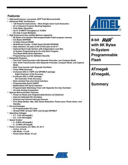
Features• High-performance, Low-power AVR ® 8-bit Microcontroller• Advanced RISC Architecture– 130 Powerful Instructions – Most Single-clock Cycle Execution– 32 x 8 General Purpose Working Registers– Fully Static Operation– Up to 16 MIPS Throughput at 16 MHz– On-chip 2-cycle Multiplier• High Endurance Non-volatile Memory segments– 8K Bytes of In-System Self-programmable Flash program memory– 512 Bytes EEPROM– 1K Byte Internal SRAM– Write/Erase Cycles: 10,000 Flash/100,000 EEPROM– Data retention: 20 years at 85°C/100 years at 25°C (1)– Optional Boot Code Section with Independent Lock BitsIn-System Programming by On-chip Boot ProgramTrue Read-While-Write Operation– Programming Lock for Software Security• Peripheral Features– Two 8-bit Timer/Counters with Separate Prescaler, one Compare Mode– One 16-bit Timer/Counter with Separate Prescaler, Compare Mode, and CaptureMode– Real Time Counter with Separate Oscillator– Three PWM Channels– 8-channel ADC in TQFP and QFN/MLF packageEight Channels 10-bit Accuracy– 6-channel ADC in PDIP packageSix Channels 10-bit Accuracy– Byte-oriented Two-wire Serial Interface– Programmable Serial USART– Master/Slave SPI Serial Interface– Programmable Watchdog Timer with Separate On-chip Oscillator– On-chip Analog Comparator• Special Microcontroller Features– Power-on Reset and Programmable Brown-out Detection– Internal Calibrated RC Oscillator– External and Internal Interrupt Sources– Five Sleep Modes: Idle, ADC Noise Reduction, Power-save, Power-down, andStandby• I/O and Packages– 23 Programmable I/O Lines– 28-lead PDIP, 32-lead TQFP, and 32-pad QFN/MLF• Operating Voltages– 2.7 - 5.5V (<strong>ATmega8</strong>L)– 4.5 - 5.5V (<strong>ATmega8</strong>)• Speed Grades– 0 - 8 MHz (<strong>ATmega8</strong>L)– 0 - 16 MHz (<strong>ATmega8</strong>)• Power Consumption at 4 Mhz, 3V, 25°C– Active: 3.6 mA– Idle Mode: 1.0 mA– Power-down Mode: 0.5 µA8-bitwith 8K BytesIn-SystemProgrammableFlash<strong>ATmega8</strong><strong>ATmega8</strong>LSummary
PinConfigurationsPDIP(RESET) PC6(RXD) PD0(TXD) PD1(INT0) PD2(INT1) PD3(XCK/T0) PD4VCCGND(XTAL1/TOSC1) PB6(XTAL2/TOSC2) PB7(T1) PD5(AIN0) PD6(AIN1) PD7(ICP1) PB012345678910111213142827262524232221201918171615PC5 (ADC5/SCL)PC4 (ADC4/SDA)PC3 (ADC3)PC2 (ADC2)PC1 (ADC1)PC0 (ADC0)GNDAREFAVCCPB5 (SCK)PB4 (MISO)PB3 (MOSI/OC2)PB2 (SS/OC1B)PB1 (OC1A)TQFP Top View3231302928272625(INT1) PD3(XCK/T0) PD4GNDVCCGNDVCC(XTAL1/TOSC1) PB6(XTAL2/TOSC2) PB7123456782423222120191817PC1 (ADC1)PC0 (ADC0)ADC7GNDAREFADC6AVCCPB5 (SCK)(T1) PD5(AIN0) PD6(AIN1) PD7(ICP1) PB0(OC1A) PB1(SS/OC1B) PB2(MOSI/OC2) PB3(MISO) PB4910111213141516PD2 (INT0)PD1 (TXD)PD0 (RXD)PC6 (RESET)PC5 (ADC5/SCL)PC4 (ADC4/SDA)PC3 (ADC3)PC2 (ADC2)MLF Top View3231302928272625(INT1) PD3(XCK/T0) PD4GNDVCCGNDVCC(XTAL1/TOSC1) PB6(XTAL2/TOSC2) PB7123456782423222120191817PC1 (ADC1)PC0 (ADC0)ADC7GNDAREFADC6AVCCPB5 (SCK)910111213141516PD2 (INT0)PD1 (TXD)PD0 (RXD)PC6 (RESET)PC5 (ADC5/SCL)PC4 (ADC4/SDA)PC3 (ADC3)PC2 (ADC2)(T1) PD5(AIN0) PD6(AIN1) PD7(ICP1) PB0(OC1A) PB1(SS/OC1B) PB2(MOSI/OC2) PB3(MISO) PB4NOTE:The large center pad underneath the MLFpackages is made of metal and internallyconnected to GND. It should be solderedor glued to the PCB to ensure goodmechanical stability. If the center pad isleft unconneted, the package mightloosen from the PCB.2<strong>ATmega8</strong>(L)2486SS–AVR–08/07
<strong>ATmega8</strong>(L)Pin DescriptionsVCCGNDPort B (PB7..PB0)XTAL1/XTAL2/TOSC1/TOSC2Port C (PC5..PC0)PC6/RESETPort D (PD7..PD0)RESETDigital supply voltage.Ground.Port B is an 8-bit bi-directional I/O port with internal pull-up resistors (selected for each bit). ThePort B output buffers have symmetrical drive characteristics with both high sink and sourcecapability. As inputs, Port B pins that are externally pulled low will source current if the pull-upresistors are activated. The Port B pins are tri-stated when a reset condition becomes active,even if the clock is not running.Depending on the clock selection fuse settings, PB6 can be used as input to the inverting Oscillatoramplifier and input to the internal clock operating circuit.Depending on the clock selection fuse settings, PB7 can be used as output from the invertingOscillator amplifier.If the Internal Calibrated RC Oscillator is used as chip clock source, PB7..6 is used as TOSC2..1input for the Asynchronous Timer/Counter2 if the AS2 bit in ASSR is set.The various special features of Port B are elaborated in “Alternate Functions of Port B” on page58 and “System Clock and Clock Options” on page 25.Port C is an 7-bit bi-directional I/O port with internal pull-up resistors (selected for each bit). ThePort C output buffers have symmetrical drive characteristics with both high sink and sourcecapability. As inputs, Port C pins that are externally pulled low will source current if the pull-upresistors are activated. The Port C pins are tri-stated when a reset condition becomes active,even if the clock is not running.If the RSTDISBL Fuse is programmed, PC6 is used as an I/O pin. Note that the electrical characteristicsof PC6 differ from those of the other pins of Port C.If the RSTDISBL Fuse is unprogrammed, PC6 is used as a Reset input. A low level on this pinfor longer than the minimum pulse length will generate a Reset, even if the clock is not running.The minimum pulse length is given in Table 15 on page 38. Shorter pulses are not guaranteed togenerate a Reset.The various special features of Port C are elaborated on page 61.Port D is an 8-bit bi-directional I/O port with internal pull-up resistors (selected for each bit). ThePort D output buffers have symmetrical drive characteristics with both high sink and sourcecapability. As inputs, Port D pins that are externally pulled low will source current if the pull-upresistors are activated. The Port D pins are tri-stated when a reset condition becomes active,even if the clock is not running.Port D also serves the functions of various special features of the <strong>ATmega8</strong> as listed on page63.Reset input. A low level on this pin for longer than the minimum pulse length will generate areset, even if the clock is not running. The minimum pulse length is given in Table 15 on page38. Shorter pulses are not guaranteed to generate a reset.2486SS–AVR–08/075
AV CCAREFADC7..6 (TQFP andQFN/MLF PackageOnly)AV CC is the supply voltage pin for the A/D Converter, Port C (3..0), and ADC (7..6). It should beexternally connected to V CC , even if the ADC is not used. If the ADC is used, it should be connectedto V CC through a low-pass filter. Note that Port C (5..4) use digital supply voltage, V CC .AREF is the analog reference pin for the A/D Converter.In the TQFP and QFN/MLF package, ADC7..6 serve as analog inputs to the A/D converter.These pins are powered from the analog supply and serve as 10-bit ADC channels.6<strong>ATmega8</strong>(L)2486SS–AVR–08/07
<strong>ATmega8</strong>(L)ResourcesData RetentionA comprehensive set of development tools, application notes and datasheets are available fordownload on http://www.atmel.com/avr.Note: 1.Reliability Qualification results show that the projected data retention failure rate is much lessthan 1 PPM over 20 years at 85°C or 100 years at 25°C.2486SS–AVR–08/077
Register SummaryAddress Name Bit 7 Bit 6 Bit 5 Bit 4 Bit 3 Bit 2 Bit 1 Bit 0 Page0x3F (0x5F) SREG I T H S V N Z C 110x3E (0x5E) SPH – – – – – SP10 SP9 SP8 130x3D (0x5D) SPL SP7 SP6 SP5 SP4 SP3 SP2 SP1 SP0 130x3C (0x5C) Reserved0x3B (0x5B) GICR INT1 INT0 – – – – IVSEL IVCE 49, 670x3A (0x5A) GIFR INTF1 INTF0 – – – – – – 680x39 (0x59) TIMSK OCIE2 TOIE2 TICIE1 OCIE1A OCIE1B TOIE1 – TOIE0 72, 102, 1220x38 (0x58) TIFR OCF2 TOV2 ICF1 OCF1A OCF1B TOV1 – TOV0 73, 102, 1220x37 (0x57) SPMCR SPMIE RWWSB – RWWSRE BLBSET PGWRT PGERS SPMEN 2130x36 (0x56) TWCR TWINT TWEA TWSTA TWSTO TWWC TWEN – TWIE 1710x35 (0x55) MCUCR SE SM2 SM1 SM0 ISC11 ISC10 ISC01 ISC00 33, 660x34 (0x54) MCUCSR – – – – WDRF BORF EXTRF PORF 410x33 (0x53) TCCR0 – – – – – CS02 CS01 CS00 720x32 (0x52) TCNT0 Timer/Counter0 (8 Bits) 720x31 (0x51) OSCCAL Oscillator Calibration Register 310x30 (0x50) SFIOR – – – – ACME PUD PSR2 PSR10 58, 75, 123, 1930x2F (0x4F) TCCR1A COM1A1 COM1A0 COM1B1 COM1B0 FOC1A FOC1B WGM11 WGM10 960x2E (0x4E) TCCR1B ICNC1 ICES1 – WGM13 WGM12 CS12 CS11 CS10 1000x2D (0x4D) TCNT1H Timer/Counter1 – Counter Register High byte 1010x2C (0x4C) TCNT1L Timer/Counter1 – Counter Register Low byte 1010x2B (0x4B) OCR1AH Timer/Counter1 – Output Compare Register A High byte 1010x2A (0x4A) OCR1AL Timer/Counter1 – Output Compare Register A Low byte 1010x29 (0x49) OCR1BH Timer/Counter1 – Output Compare Register B High byte 1010x28 (0x48) OCR1BL Timer/Counter1 – Output Compare Register B Low byte 1010x27 (0x47) ICR1H Timer/Counter1 – Input Capture Register High byte 1020x26 (0x46) ICR1L Timer/Counter1 – Input Capture Register Low byte 1020x25 (0x45) TCCR2 FOC2 WGM20 COM21 COM20 WGM21 CS22 CS21 CS20 1170x24 (0x44) TCNT2 Timer/Counter2 (8 Bits) 1190x23 (0x43) OCR2 Timer/Counter2 Output Compare Register 1190x22 (0x42) ASSR – – – – AS2 TCN2UB OCR2UB TCR2UB 1190x21 (0x41) WDTCR – – – WDCE WDE WDP2 WDP1 WDP0 430x20 (1) (0x40) (1) UBRRH URSEL – – – UBRR[11:8] 158UCSRC URSEL UMSEL UPM1 UPM0 USBS UCSZ1 UCSZ0 UCPOL 1560x1F (0x3F) EEARH – – – – – – – EEAR8 200x1E (0x3E) EEARL EEAR7 EEAR6 EEAR5 EEAR4 EEAR3 EEAR2 EEAR1 EEAR0 200x1D (0x3D) EEDR EEPROM Data Register 200x1C (0x3C) EECR – – – – EERIE EEMWE EEWE EERE 200x1B (0x3B) Reserved0x1A (0x3A) Reserved0x19 (0x39) Reserved0x18 (0x38) PORTB PORTB7 PORTB6 PORTB5 PORTB4 PORTB3 PORTB2 PORTB1 PORTB0 650x17 (0x37) DDRB DDB7 DDB6 DDB5 DDB4 DDB3 DDB2 DDB1 DDB0 650x16 (0x36) PINB PINB7 PINB6 PINB5 PINB4 PINB3 PINB2 PINB1 PINB0 650x15 (0x35) PORTC – PORTC6 PORTC5 PORTC4 PORTC3 PORTC2 PORTC1 PORTC0 650x14 (0x34) DDRC – DDC6 DDC5 DDC4 DDC3 DDC2 DDC1 DDC0 650x13 (0x33) PINC – PINC6 PINC5 PINC4 PINC3 PINC2 PINC1 PINC0 650x12 (0x32) PORTD PORTD7 PORTD6 PORTD5 PORTD4 PORTD3 PORTD2 PORTD1 PORTD0 650x11 (0x31) DDRD DDD7 DDD6 DDD5 DDD4 DDD3 DDD2 DDD1 DDD0 650x10 (0x30) PIND PIND7 PIND6 PIND5 PIND4 PIND3 PIND2 PIND1 PIND0 650x0F (0x2F) SPDR SPI Data Register 1310x0E (0x2E) SPSR SPIF WCOL – – – – – SPI2X 1310x0D (0x2D) SPCR SPIE SPE DORD MSTR CPOL CPHA SPR1 SPR0 1290x0C (0x2C) UDR USART I/O Data Register 1530x0B (0x2B) UCSRA RXC TXC UDRE FE DOR PE U2X MPCM 1540x0A (0x2A) UCSRB RXCIE TXCIE UDRIE RXEN TXEN UCSZ2 RXB8 TXB8 1550x09 (0x29) UBRRL USART Baud Rate Register Low byte 1580x08 (0x28) ACSR ACD ACBG ACO ACI ACIE ACIC ACIS1 ACIS0 1940x07 (0x27) ADMUX REFS1 REFS0 ADLAR – MUX3 MUX2 MUX1 MUX0 2050x06 (0x26) ADCSRA ADEN ADSC ADFR ADIF ADIE ADPS2 ADPS1 ADPS0 2070x05 (0x25) ADCH ADC Data Register High byte 2080x04 (0x24) ADCL ADC Data Register Low byte 2080x03 (0x23) TWDR Two-wire Serial Interface Data Register 1730x02 (0x22) TWAR TWA6 TWA5 TWA4 TWA3 TWA2 TWA1 TWA0 TWGCE 1748<strong>ATmega8</strong>(L)2486SS–AVR–08/07
<strong>ATmega8</strong>(L)Register Summary (Continued)Address Name Bit 7 Bit 6 Bit 5 Bit 4 Bit 3 Bit 2 Bit 1 Bit 0 Page0x01 (0x21) TWSR TWS7 TWS6 TWS5 TWS4 TWS3 – TWPS1 TWPS0 1730x00 (0x20) TWBR Two-wire Serial Interface Bit Rate Register 171Notes: 1. Refer to the USART description for details on how to access UBRRH and UCSRC.2. For compatibility with future devices, reserved bits should be written to zero if accessed. Reserved I/O memory addressesshould never be written.3. Some of the Status Flags are cleared by writing a logical one to them. Note that the CBI and SBI instructions will operate onall bits in the I/O Register, writing a one back into any flag read as set, thus clearing the flag. The CBI and SBI instructionswork with registers 0x00 to 0x1F only.2486SS–AVR–08/079
Instruction Set SummaryMnemonics Operands Description Operation Flags #ClocksARITHMETIC AND LOGIC INSTRUCTIONSADD Rd, Rr Add two Registers Rd ← Rd + Rr Z,C,N,V,H 1ADC Rd, Rr Add with Carry two Registers Rd ← Rd + Rr + C Z,C,N,V,H 1ADIW Rdl,K Add Immediate to Word Rdh:Rdl ← Rdh:Rdl + K Z,C,N,V,S 2SUB Rd, Rr Subtract two Registers Rd ← Rd - Rr Z,C,N,V,H 1SUBI Rd, K Subtract Constant from Register Rd ← Rd - K Z,C,N,V,H 1SBC Rd, Rr Subtract with Carry two Registers Rd ← Rd - Rr - C Z,C,N,V,H 1SBCI Rd, K Subtract with Carry Constant from Reg. Rd ← Rd - K - C Z,C,N,V,H 1SBIW Rdl,K Subtract Immediate from Word Rdh:Rdl ← Rdh:Rdl - K Z,C,N,V,S 2AND Rd, Rr Logical AND Registers Rd ← Rd • Rr Z,N,V 1ANDI Rd, K Logical AND Register and Constant Rd ← Rd • K Z,N,V 1OR Rd, Rr Logical OR Registers Rd ← Rd v Rr Z,N,V 1ORI Rd, K Logical OR Register and Constant Rd ← Rd v K Z,N,V 1EOR Rd, Rr Exclusive OR Registers Rd ← Rd ⊕ Rr Z,N,V 1COM Rd One’s Complement Rd ← 0xFF − Rd Z,C,N,V 1NEG Rd Two’s Complement Rd ← 0x00 − Rd Z,C,N,V,H 1SBR Rd,K Set Bit(s) in Register Rd ← Rd v K Z,N,V 1CBR Rd,K Clear Bit(s) in Register Rd ← Rd • (0xFF - K) Z,N,V 1INC Rd Increment Rd ← Rd + 1 Z,N,V 1DEC Rd Decrement Rd ← Rd − 1 Z,N,V 1TST Rd Test for Zero or Minus Rd ← Rd • Rd Z,N,V 1CLR Rd Clear Register Rd ← Rd ⊕ Rd Z,N,V 1SER Rd Set Register Rd ← 0xFF None 1MUL Rd, Rr Multiply Unsigned R1:R0 ← Rd x Rr Z,C 2MULS Rd, Rr Multiply Signed R1:R0 ← Rd x Rr Z,C 2MULSU Rd, Rr Multiply Signed with Unsigned R1:R0 ← Rd x Rr Z,C 2FMUL Rd, Rr Fractional Multiply Unsigned R1:R0 ← (Rd x Rr)
<strong>ATmega8</strong>(L)Instruction Set Summary (Continued)BRIE k Branch if Interrupt Enabled if ( I = 1) then PC ← PC + k + 1 None 1 / 2BRID k Branch if Interrupt Disabled if ( I = 0) then PC ← PC + k + 1 None 1 / 2DATA TRANSFER INSTRUCTIONSMOV Rd, Rr Move Between Registers Rd ← Rr None 1MOVW Rd, Rr Copy Register Word Rd+1:Rd ← Rr+1:Rr None 1LDI Rd, K Load Immediate Rd ← K None 1LD Rd, X Load Indirect Rd ← (X) None 2LD Rd, X+ Load Indirect and Post-Inc. Rd ← (X), X ← X + 1 None 2LD Rd, - X Load Indirect and Pre-Dec. X ← X - 1, Rd ← (X) None 2LD Rd, Y Load Indirect Rd ← (Y) None 2LD Rd, Y+ Load Indirect and Post-Inc. Rd ← (Y), Y ← Y + 1 None 2LD Rd, - Y Load Indirect and Pre-Dec. Y ← Y - 1, Rd ← (Y) None 2LDD Rd,Y+q Load Indirect with Displacement Rd ← (Y + q) None 2LD Rd, Z Load Indirect Rd ← (Z) None 2LD Rd, Z+ Load Indirect and Post-Inc. Rd ← (Z), Z ← Z+1 None 2LD Rd, -Z Load Indirect and Pre-Dec. Z ← Z - 1, Rd ← (Z) None 2LDD Rd, Z+q Load Indirect with Displacement Rd ← (Z + q) None 2LDS Rd, k Load Direct from SRAM Rd ← (k) None 2ST X, Rr Store Indirect (X) ← Rr None 2ST X+, Rr Store Indirect and Post-Inc. (X) ← Rr, X ← X + 1 None 2ST - X, Rr Store Indirect and Pre-Dec. X ← X - 1, (X) ← Rr None 2ST Y, Rr Store Indirect (Y) ← Rr None 2ST Y+, Rr Store Indirect and Post-Inc. (Y) ← Rr, Y ← Y + 1 None 2ST - Y, Rr Store Indirect and Pre-Dec. Y ← Y - 1, (Y) ← Rr None 2STD Y+q,Rr Store Indirect with Displacement (Y + q) ← Rr None 2ST Z, Rr Store Indirect (Z) ← Rr None 2ST Z+, Rr Store Indirect and Post-Inc. (Z) ← Rr, Z ← Z + 1 None 2ST -Z, Rr Store Indirect and Pre-Dec. Z ← Z - 1, (Z) ← Rr None 2STD Z+q,Rr Store Indirect with Displacement (Z + q) ← Rr None 2STS k, Rr Store Direct to SRAM (k) ← Rr None 2LPM Load Program Memory R0 ← (Z) None 3LPM Rd, Z Load Program Memory Rd ← (Z) None 3LPM Rd, Z+ Load Program Memory and Post-Inc Rd ← (Z), Z ← Z+1 None 3SPM Store Program Memory (Z) ← R1:R0 None -IN Rd, P In Port Rd ← P None 1OUT P, Rr Out Port P ← Rr None 1PUSH Rr Push Register on Stack STACK ← Rr None 2POP Rd Pop Register from Stack Rd ← STACK None 2BIT AND BIT-TEST INSTRUCTIONSSBI P,b Set Bit in I/O Register I/O(P,b) ← 1 None 2CBI P,b Clear Bit in I/O Register I/O(P,b) ← 0 None 2LSL Rd Logical Shift Left Rd(n+1) ← Rd(n), Rd(0) ← 0 Z,C,N,V 1LSR Rd Logical Shift Right Rd(n) ← Rd(n+1), Rd(7) ← 0 Z,C,N,V 1ROL Rd Rotate Left Through Carry Rd(0)←C,Rd(n+1)← Rd(n),C←Rd(7) Z,C,N,V 1ROR Rd Rotate Right Through Carry Rd(7)←C,Rd(n)← Rd(n+1),C←Rd(0) Z,C,N,V 1ASR Rd Arithmetic Shift Right Rd(n) ← Rd(n+1), n=0..6 Z,C,N,V 1SWAP Rd Swap Nibbles Rd(3..0)←Rd(7..4),Rd(7..4)←Rd(3..0) None 1BSET s Flag Set SREG(s) ← 1 SREG(s) 1BCLR s Flag Clear SREG(s) ← 0 SREG(s) 1BST Rr, b Bit Store from Register to T T ← Rr(b) T 1BLD Rd, b Bit load from T to Register Rd(b) ← T None 1SEC Set Carry C ← 1 C 1CLC Clear Carry C ← 0 C 1SEN Set Negative Flag N ← 1 N 1CLN Clear Negative Flag N ← 0 N 1SEZ Set Zero Flag Z ← 1 Z 1CLZ Clear Zero Flag Z ← 0 Z 1SEI Global Interrupt Enable I ← 1 I 1CLI Global Interrupt Disable I ← 0 I 1SES Set Signed Test Flag S ← 1 S 1CLS Clear Signed Test Flag S ← 0 S 1SEV Set Twos Complement Overflow. V ← 1 V 1CLV Clear Twos Complement Overflow V ← 0 V 1SET Set T in SREG T ← 1 T 1Mnemonics Operands Description Operation Flags #Clocks2486SS–AVR–08/0711
Instruction Set Summary (Continued)CLT Clear T in SREG T ← 0 T 1SEH Set Half Carry Flag in SREG H ← 1 H 1CLH Clear Half Carry Flag in SREG H ← 0 H 1MCU CONTROL INSTRUCTIONSNOP No Operation None 1SLEEP Sleep (see specific descr. for Sleep function) None 1WDR Watchdog Reset (see specific descr. for WDR/timer) None 112<strong>ATmega8</strong>(L)2486SS–AVR–08/07
<strong>ATmega8</strong>(L)Ordering InformationSpeed (MHz) Power Supply Ordering Code Package (1) Operation Range8 2.7 - 5.516 4.5 - 5.5<strong>ATmega8</strong>L-8AC<strong>ATmega8</strong>L-8PC<strong>ATmega8</strong>L-8MC<strong>ATmega8</strong>L-8AI<strong>ATmega8</strong>L-8AU (2)<strong>ATmega8</strong>L-8PI<strong>ATmega8</strong>L-8PU (2)<strong>ATmega8</strong>L-8MI<strong>ATmega8</strong>L-8MU (2)<strong>ATmega8</strong>-16AC<strong>ATmega8</strong>-16PC<strong>ATmega8</strong>-16MC<strong>ATmega8</strong>-16AI<strong>ATmega8</strong>-16AU (2)<strong>ATmega8</strong>-16PI<strong>ATmega8</strong>-16PU (2)<strong>ATmega8</strong>-16MI<strong>ATmega8</strong>-16MU (2)32A28P332M1-A32A32A28P328P332M1-A32M1-A32A28P332M1-A32A32A28P328P332M1-A32M1-ACommercial(0°C to 70°C)Industrial(-40°C to 85°C)Commercial(0°C to 70°C)Industrial(-40°C to 85°C)Notes: 1. This device can also be supplied in wafer form. Please contact your local Atmel sales office for detailed ordering informationand minimum quantities.2. Pb-free packaging alternative, complies to the European Directive for Restriction of Hazardous Substances (RoHS directive).Also Halide free and fully Green.Package Type32A28P332M1-A32-lead, Thin (1.0 mm) Plastic Quad Flat Package (TQFP)28-lead, 0.300” Wide, Plastic Dual Inline Package (PDIP)32-pad, 5 x 5 x 1.0 body, Lead Pitch 0.50 mm Quad Flat No-Lead/Micro Lead Frame Package (QFN/MLF)2486SS–AVR–08/0713
Packaging Information32APIN 1PIN 1 IDENTIFIERBe E1 ED1DC0˚~7˚LA1 A2 ACOMMON DIMENSIONS(Unit of Measure = mm)Notes:1. This package conforms to JEDEC reference MS-026, Variation ABA.2. Dimensions D1 and E1 do not include mold protrusion. Allowableprotrusion is 0.25 mm per side. Dimensions D1 and E1 are maximumplastic body size dimensions including mold mismatch.3. Lead coplanarity is 0.10 mm maximum.SYMBOL MIN NOM MAX NOTEA – – 1.20A1 0.05 – 0.15A2 0.95 1.00 1.05D 8.75 9.00 9.25D1 6.90 7.00 7.10 Note 2E 8.75 9.00 9.25E1 6.90 7.00 7.10 Note 2B 0.30 – 0.45C 0.09 – 0.20L 0.45 – 0.75e0.80 TYP10/5/2001R2325 Orchard ParkwaySan Jose, CA 95131TITLE32A, 32-lead, 7 x 7 mm Body Size, 1.0 mm Body Thickness,0.8 mm Lead Pitch, Thin Profile Plastic Quad Flat Package (TQFP)DRAWING NO.32AREV.B14<strong>ATmega8</strong>(L)2486SS–AVR–08/07
<strong>ATmega8</strong>(L)28P3DPIN1E1ASEATING PLANELeB1BA1B2(4 PLACES)Note:CEeB0º ~ 15º1. Dimensions D and E1 do not include mold Flash or Protrusion.Mold Flash or Protrusion shall not exceed 0.25 mm (0.010").REFCOMMON DIMENSIONS(Unit of Measure = mm)SYMBOL MIN NOM MAX NOTEA – – 4.5724A1 0.508 – –D 34.544 – 34.798 Note 1E 7.620 – 8.255E1 7.112 – 7.493 Note 1B 0.381 – 0.533B1 1.143 – 1.397B2 0.762 – 1.143L 3.175 – 3.429C 0.203 – 0.356eB – – 10.160e2.540 TYP09/28/01R2325 Orchard ParkwaySan Jose, CA 95131TITLE28P3, 28-lead (0.300"/7.62 mm Wide) Plastic DualInline Package (PDIP)DRAWING NO.28P3REV.B2486SS–AVR–08/0715
32M1-ADD1123Pin 1 ID0E1ESIDE VIEWPPbTOP VIEWKD2Pin #1 Notch(0.20 R)BOTTOM VIEWe123Note: JEDEC Standard MO-220, Fig. 2 (Anvil Singulation), VHHD-2.E2LKA2AA3A10.08 CCOMMON DIMENSIONS(Unit of Measure = mm)SYMBOL MIN NOM MAX NOTEA 0.80 0.90 1.00A1 – 0.02 0.05A2 – 0.65 1.00A30.20 REFb 0.18 0.23 0.30D 4.90 5.00 5.10D1 4.70 4.75 4.80D2 2.95 3.10 3.25E 4.90 5.00 5.10E1 4.70 4.75 4.80E2 2.95 3.10 3.25e0.50 BSCL 0.30 0.40 0.50P – – 0.600 – – 12 oK 0.20 – –5/25/06R2325 Orchard ParkwaySan Jose, CA 95131TITLE32M1-A, 32-pad, 5 x 5 x 1.0 mm Body, Lead Pitch 0.50 mm,3.10 mm Exposed Pad, Micro Lead Frame Package (MLF)DRAWING NO.32M1-AREV.E16<strong>ATmega8</strong>(L)2486SS–AVR–08/07
<strong>ATmega8</strong>(L)Errata<strong>ATmega8</strong>Rev. D to IThe revision letter in this section refers to the revision of the <strong>ATmega8</strong> device.• First Analog Comparator conversion may be delayed• Interrupts may be lost when writing the timer registers in the asynchronous timer• Signature may be Erased in Serial Programming Mode• CKOPT Does not Enable Internal Capacitors on XTALn/TOSCn Pins when 32 KHz Oscillator isUsed to Clock the Asynchronous Timer/Counter2• Reading EEPROM by using ST or STS to set EERE bit triggers unexpected interrupt request1. First Analog Comparator conversion may be delayedIf the device is powered by a slow rising V CC , the first Analog Comparator conversion willtake longer than expected on some devices.Problem Fix / WorkaroundWhen the device has been powered or reset, disable then enable theAnalog Comparatorbefore the first conversion.2. Interrupts may be lost when writing the timer registers in the asynchronous timerIf one of the timer registers which is synchronized to the asynchronous timer2 clock is writtenin the cycle before a overflow interrupt occurs, the interrupt may be lost.Problem Fix / WorkaroundAlways check that the Timer2 Timer/Counter register, TCNT2, does not have the value 0xFFbefore writing the Timer2 Control Register, TCCR2, or Output Compare Register, OCR23. Signature may be Erased in Serial Programming ModeIf the signature bytes are read before a chiperase command is completed, the signature maybe erased causing the device ID and calibration bytes to disappear. This is critical, especially,if the part is running on internal RC oscillator.Problem Fix / Workaround:Ensure that the chiperase command has exceeded before applying the next command.4. CKOPT Does not Enable Internal Capacitors on XTALn/TOSCn Pins when 32 KHzOscillator is Used to Clock the Asynchronous Timer/Counter2When the internal RC Oscillator is used as the main clock source, it is possible to run theTimer/Counter2 asynchronously by connecting a 32 KHz Oscillator between XTAL1/TOSC1and XTAL2/TOSC2. But when the internal RC Oscillator is selected as the main clocksource, the CKOPT Fuse does not control the internal capacitors on XTAL1/TOSC1 andXTAL2/TOSC2. As long as there are no capacitors connected to XTAL1/TOSC1 andXTAL2/TOSC2, safe operation of the Oscillator is not guaranteed.Problem Fix / WorkaroundUse external capacitors in the range of 20 - 36 pF on XTAL1/TOSC1 and XTAL2/TOSC2.This will be fixed in <strong>ATmega8</strong> Rev. G where the CKOPT Fuse will control internal capacitorsalso when internal RC Oscillator is selected as main clock source. For <strong>ATmega8</strong> Rev. G,CKOPT = 0 (programmed) will enable the internal capacitors on XTAL1 and XTAL2. Customerswho want compatibility between Rev. G and older revisions, must ensure thatCKOPT is unprogrammed (CKOPT = 1).5. Reading EEPROM by using ST or STS to set EERE bit triggers unexpected interruptrequest.Reading EEPROM by using the ST or STS command to set the EERE bit in the EECR registertriggers an unexpected EEPROM interrupt request.2486SS–AVR–08/0717
Problem Fix / WorkaroundAlways use OUT or SBI to set EERE in EECR.18<strong>ATmega8</strong>(L)2486SS–AVR–08/07
<strong>ATmega8</strong>(L)DatasheetRevisionHistoryChanges from Rev.2486R- 07/07 toRev. 2486S- 08/07Please note that the referring page numbers in this section are referred to this document. Thereferring revision in this section are referring to the document revision.1. Updated “Features” on page 1.2. Added “Data Retention” on page 7.3. Updated “Errata” on page 17.4. Updated “Slave Mode” on page 129.Changes from Rev.2486Q- 10/06 toRev. 2486R- 07/071. Added text to Table 81 on page 218.2. Fixed typo in “Peripheral Features” on page 1.3. Updated Table 16 on page 42.4. Updated Table 75 on page 206.5. Removed redundancy and updated typo in Notes section of “DC Characteristics” onpage 242.Changes from Rev.2486P- 02/06 toRev. 2486Q- 10/061. Updated “Timer/Counter Oscillator” on page 32.2. Updated “Fast PWM Mode” on page 89.3. Updated code example in “USART Initialization” on page 138.4. Updated Table 37 on page 97, Table 39 on page 98, Table 42 on page 117, Table 44 onpage 118, and Table 98 on page 240.5. Updated “Errata” on page 17.Changes from Rev.2486O-10/04 toRev. 2486P- 02/061. Added “Resources” on page 7.2. Updated “External Clock” on page 32.3. Updated “Serial Peripheral Interface – SPI” on page 124.4. Updated Code Example in “USART Initialization” on page 138.5. Updated Note in “Bit Rate Generator Unit” on page 170.6. Updated Table 98 on page 240.7. Updated Note in Table 103 on page 248.8. Updated “Errata” on page 17.2486SS–AVR–08/0719
Changes from Rev.2486N-09/04 toRev. 2486O-10/041. Removed to instances of “analog ground”. Replaced by “ground”.2. Updated Table 7 on page 29, Table 15 on page 38, and Table 100 on page 244.3. Updated “Calibrated Internal RC Oscillator” on page 30 with the 1 MHz default value.4. Table 89 on page 225 and Table 90 on page 225 moved to new section “Page Size” onpage 225.5. Updated descripton for bit 4 in “Store Program Memory Control Register – SPMCR”on page 213.6. Updated “Ordering Information” on page 13.Changes from Rev.2486M-12/03 toRev. 2486N-09/041. Added note to MLF package in “Pin Configurations” on page 2.2. Updated “Internal Voltage Reference Characteristics” on page 42.3. Updated “DC Characteristics” on page 242.4. ADC4 and ADC5 support 10-bit accuracy. Document updated to reflect this.Updated features in “Analog-to-Digital Converter” on page 196.Updated “ADC Characteristics” on page 248.5. Removed reference to “External RC Oscillator application note” from “External RCOscillator” on page 28.Changes from Rev.2486L-10/03 toRev. 2486M-12/03Changes from Rev.2486K-08/03 toRev. 2486L-10/031. Updated “Calibrated Internal RC Oscillator” on page 30.1. Removed “Preliminary” and TBDs from the datasheet.2. Renamed ICP to ICP1 in the datasheet.3. Removed instructions CALL and JMP from the datasheet.4. Updated t RST in Table 15 on page 38, V BG in Table 16 on page 42, Table 100 on page244 and Table 102 on page 246.5. Replaced text “XTAL1 and XTAL2 should be left unconnected (NC)” after Table 9 in“Calibrated Internal RC Oscillator” on page 30. Added text regarding XTAL1/XTAL2and CKOPT Fuse in “Timer/Counter Oscillator” on page 32.6. Updated Watchdog Timer code examples in “Timed Sequences for Changing theConfiguration of the Watchdog Timer” on page 45.7. Removed bit 4, ADHSM, from “Special Function IO Register – SFIOR” on page 58.8. Added note 2 to Figure 103 on page 215.9. Updated item 4 in the “Serial Programming Algorithm” on page 238.20<strong>ATmega8</strong>(L)2486SS–AVR–08/07
<strong>ATmega8</strong>(L)10. Added t WD_FUSE to Table 97 on page 239 and updated Read Calibration Byte, Byte 3, inTable 98 on page 240.11. Updated Absolute Maximum Ratings* and DC Characteristics in “Electrical Characteristics”on page 242.Changes from Rev.2486J-02/03 toRev. 2486K-08/031. Updated V BOT values in Table 15 on page 38.2. Updated “ADC Characteristics” on page 248.3. Updated “<strong>ATmega8</strong> Typical Characteristics” on page 249.4. Updated “Errata” on page 17.Changes from Rev.2486I-12/02 to Rev.2486J-02/031. Improved the description of “Asynchronous Timer Clock – clkASY” on page 26.2. Removed reference to the “Multipurpose Oscillator” application note and the “32 kHzCrystal Oscillator” application note, which do not exist.3. Corrected OCn waveforms in Figure 38 on page 90.4. Various minor Timer 1 corrections.5. Various minor TWI corrections.6. Added note under “Filling the Temporary Buffer (Page Loading)” on page 216 aboutwriting to the EEPROM during an SPM Page load.7. Removed ADHSM completely.8. Added section “EEPROM Write during Power-down Sleep Mode” on page 23.9. Removed XTAL1 and XTAL2 description on page 5 because they were alreadydescribed as part of “Port B (PB7..PB0) XTAL1/XTAL2/TOSC1/TOSC2” on page 5.10. Improved the table under “SPI Timing Characteristics” on page 246 and removed thetable under “SPI Serial Programming Characteristics” on page 241.11. Corrected PC6 in “Alternate Functions of Port C” on page 61.12. Corrected PB6 and PB7 in “Alternate Functions of Port B” on page 58.13. Corrected 230.4 Mbps to 230.4 kbps under “Examples of Baud Rate Setting” on page159.14. Added information about PWM symmetry for Timer 2 in “Phase Correct PWM Mode”on page 113.15. Added thick lines around accessible registers in Figure 76 on page 169.16. Changed “will be ignored” to “must be written to zero” for unused Z-pointer bitsunder “Performing a Page Write” on page 216.2486SS–AVR–08/0721
17. Added note for RSTDISBL Fuse in Table 87 on page 223.18. Updated drawings in “Packaging Information” on page 14.Changes from Rev.2486H-09/02 toRev. 2486I-12/02Changes from Rev.2486G-09/02 toRev. 2486H-09/02Changes from Rev.2486F-07/02 toRev. 2486G-09/02Changes from Rev.2486E-06/02 toRev. 2486F-07/021. Added errata for Rev D, E, and F on page 17.1. Changed the Endurance on the Flash to 10,000 Write/Erase Cycles.1. Updated Table 103, “ADC Characteristics,” on page 248.1. Changes in “Digital Input Enable and Sleep Modes” on page 55.2. Addition of OCS2 in “MOSI/OC2 – Port B, Bit 3” on page 59.3. The following tables have been updated:Table 51, “CPOL and CPHA Functionality,” on page 132, Table 59, “UCPOL Bit Settings,”on page 158, Table 72, “Analog Comparator Multiplexed Input(1),” on page 195, Table 73,“ADC Conversion Time,” on page 200, Table 75, “Input Channel Selections,” on page 206,and Table 84, “Explanation of Different Variables used in Figure 103 and the Mapping to theZ-pointer,” on page 221.4. Changes in “Reading the Calibration Byte” on page 234.5. Corrected Errors in Cross References.Changes from Rev.2486D-03/02 toRev. 2486E-06/021. Updated Some Preliminary Test Limits and Characterization DataThe following tables have been updated:Table 15, “Reset Characteristics,” on page 38, Table 16, “Internal Voltage Reference Characteristics,”on page 42, DC Characteristics on page 242, Table , “ADC Characteristics,” onpage 248.2. Changes in External Clock FrequencyAdded the description at the end of “External Clock” on page 32.Added period changing data in Table 99, “External Clock Drive,” on page 244.3. Updated TWI ChapterMore details regarding use of the TWI bit rate prescaler and a Table 65, “TWI Bit Rate Prescaler,”on page 173.Changes from Rev.2486C-03/02 toRev. 2486D-03/021. Updated Typical Start-up Times.The following tables has been updated:Table 5, “Start-up Times for the Crystal Oscillator Clock Selection,” on page 28, Table 6,“Start-up Times for the Low-frequency Crystal Oscillator Clock Selection,” on page 28,22<strong>ATmega8</strong>(L)2486SS–AVR–08/07
<strong>ATmega8</strong>(L)Table 8, “Start-up Times for the External RC Oscillator Clock Selection,” on page 29, andTable 12, “Start-up Times for the External Clock Selection,” on page 32.2. Added “<strong>ATmega8</strong> Typical Characteristics” on page 249.Changes from Rev.2486B-12/01 toRev. 2486C-03/021. Updated TWI Chapter.More details regarding use of the TWI Power-down operation and using the TWI as Masterwith low TWBRR values are added into the datasheet.Added the note at the end of the “Bit Rate Generator Unit” on page 170.Added the description at the end of “Address Match Unit” on page 170.2. Updated Description of OSCCAL Calibration Byte.In the datasheet, it was not explained how to take advantage of the calibration bytes for 2, 4,and 8 MHz Oscillator selections. This is now added in the following sections:Improved description of “Oscillator Calibration Register – OSCCAL” on page 31 and “CalibrationByte” on page 225.3. Added Some Preliminary Test Limits and Characterization Data.Removed some of the TBD’s in the following tables and pages:Table 3 on page 26, Table 15 on page 38, Table 16 on page 42, Table 17 on page 44, “TA =-40×C to 85×C, VCC = 2.7V to 5.5V (unless otherwise noted)” on page 242, Table 99 onpage 244, and Table 102 on page 246.4. Updated Programming Figures.Figure 104 on page 226 and Figure 112 on page 237 are updated to also reflect that AV CCmust be connected during Programming mode.5. Added a Description on how to Enter Parallel Programming Mode if RESET Pin is Disabledor if External Oscillators are Selected.Added a note in section “Enter Programming Mode” on page 228.2486SS–AVR–08/0723
HeadquartersInternationalAtmel Corporation2325 Orchard ParkwaySan Jose, CA 95131USATel: 1(408) 441-0311Fax: 1(408) 487-2600Atmel AsiaRoom 1219Chinachem Golden Plaza77 Mody Road TsimshatsuiEast KowloonHong KongTel: (852) 2721-9778Fax: (852) 2722-1369Atmel EuropeLe Krebs8, Rue Jean-Pierre TimbaudBP 30978054 Saint-Quentin-en-Yvelines CedexFranceTel: (33) 1-30-60-70-00Fax: (33) 1-30-60-71-11Atmel Japan9F, Tonetsu Shinkawa Bldg.1-24-8 ShinkawaChuo-ku, Tokyo 104-0033JapanTel: (81) 3-3523-3551Fax: (81) 3-3523-7581Product ContactWeb Sitewww.atmel.comTechnical Supportavr@atmel.comSales Contactwww.atmel.com/contactsLiterature Requestswww.atmel.com/literatureDisclaimer: The information in this document is provided in connection with Atmel products. No license, express or implied, by estoppel or otherwise, to anyintellectual property right is granted by this document or in connection with the sale of Atmel products. EXCEPT AS SET FORTH IN ATMEL’S TERMS AND CONDI-TIONS OF SALE LOCATED ON ATMEL’S WEB SITE, ATMEL ASSUMES NO LIABILITY WHATSOEVER AND DISCLAIMS ANY EXPRESS, IMPLIED OR STATUTORYWARRANTY RELATING TO ITS PRODUCTS INCLUDING, BUT NOT LIMITED TO, THE IMPLIED WARRANTY OF MERCHANTABILITY, FITNESS FOR A PARTICULARPURPOSE, OR NON-INFRINGEMENT. IN NO EVENT SHALL ATMEL BE LIABLE FOR ANY DIRECT, INDIRECT, CONSEQUENTIAL, PUNITIVE, SPECIAL OR INCIDEN-TAL DAMAGES (INCLUDING, WITHOUT LIMITATION, DAMAGES FOR LOSS OF PROFITS, BUSINESS INTERRUPTION, OR LOSS OF INFORMATION) ARISING OUT OFTHE USE OR INABILITY TO USE THIS DOCUMENT, EVEN IF ATMEL HAS BEEN ADVISED OF THE POSSIBILITY OF SUCH DAMAGES. Atmel makes norepresentations or warranties with respect to the accuracy or completeness of the contents of this document and reserves the right to make changes to specificationsand product descriptions at any time without notice. Atmel does not make any commitment to update the information contained herein. Unless specifically providedotherwise, Atmel products are not suitable for, and shall not be used in, automotive applications. Atmel’s products are not intended, authorized, or warranted for useas components in applications intended to support or sustain life.© 2007 Atmel Corporation. All rights reserved. Atmel ® , logo and combinations thereof, AVR ® and others are registered trademarks or trademarksof Atmel Corporation or its subsidiaries. Other terms and product names may be trademarks of others.2486SS–AVR–08/07


