Automatic Generation of JTAG Interface and Debug Mechanism - ICE
Automatic Generation of JTAG Interface and Debug Mechanism - ICE
Automatic Generation of JTAG Interface and Debug Mechanism - ICE

Create successful ePaper yourself
Turn your PDF publications into a flip-book with our unique Google optimized e-Paper software.
<strong>Automatic</strong> <strong>Generation</strong> <strong>of</strong> <strong>JTAG</strong> <strong>Interface</strong> <strong>and</strong> <strong>Debug</strong> <strong>Mechanism</strong> for ASIPs<br />
Oliver Schliebusch<br />
ISS, RWTH-Aachen<br />
52056 Aachen, Germany<br />
+49-241-8027884<br />
schliebu@iss.rwth-aachen.de<br />
David Kammler<br />
ISS, RWTH-Aachen<br />
52056 Aachen, Germany<br />
+49-241-8028256<br />
kammler@iss.rwth-aachen.de<br />
Rainer Leupers, Gerd Ascheid, Heinrich Meyr<br />
ISS, RWTH-Aachen, 52056 Aachen, Germany<br />
Anupam Chattopadhyay<br />
ISS, RWTH-Aachen<br />
52056 Aachen, Germany<br />
+49-241-8027871<br />
anupam@iss.rwth-aachen.de<br />
Abstract<br />
Application Specific Instruction Set Processors (ASIPs)<br />
combine the high performance <strong>of</strong> dedicated hardware with<br />
the flexibility <strong>of</strong> programmable solutions. Architecture Description<br />
Languages (ADLs) describe ASIPs on an instructionaccurate<br />
or cycle-accurate abstraction level. Accurate information<br />
about the physical parameters cannot be obtained on<br />
this level <strong>of</strong> abstraction. For this, a hardware model on Register<br />
Transfer Level (RTL) <strong>and</strong> a subsequent gate-level synthesis<br />
is required. Several projects deal with the topic <strong>of</strong> generating<br />
a hardware description model from an ADL. Currently, those<br />
approaches focus only on the desired processor core <strong>and</strong> omit<br />
architectural features, such as a debug mechanism or <strong>JTAG</strong> interface.<br />
The acceptance <strong>of</strong> ASIPs compared to other heterogenous<br />
solutions, dedicated to combine performance <strong>and</strong> flexibility,<br />
can only be achieved if well known processor features<br />
are supported. In this paper, we propose an automatic generation<br />
<strong>of</strong> <strong>JTAG</strong> interface <strong>and</strong> debug mechanism from an ADL.<br />
This generation is embedded into our RTL processor synthesis<br />
tool, which is based on the Language for Instruction Set<br />
Architectures (LISA).<br />
1 Introduction<br />
ADLs are used to map a given application to an optimized<br />
programmable architecture. These ASIPs combine high performance<br />
<strong>of</strong> dedicated hardware with the flexibility <strong>of</strong> a programmable<br />
solution. The required design space exploration<br />
is based on ADLs, which enable a fast incorporation <strong>of</strong> architectural<br />
changes. The architecture description is used to<br />
automatically derive s<strong>of</strong>tware tools, for example C-compiler,<br />
assembler, linker <strong>and</strong> simulator within a few minutes.<br />
The design space exploration, based on ADLs, is performed<br />
on a high level <strong>of</strong> abstraction <strong>and</strong> lacks accurate information<br />
about physical parameters, leading to a sub-optimal<br />
solution. These parameters (like chip area, clock speed <strong>and</strong><br />
power consumption) can be accurately derived from a hardware<br />
model on RTL <strong>and</strong> a subsequent gate-level synthesis.<br />
To obtain accurate performance figures, while preserving the<br />
speed <strong>of</strong> design space exploration using an ADL, an automated<br />
approach to generate the RTL description from the ADL<br />
is m<strong>and</strong>atory. Several projects deal with the topic <strong>of</strong> generating<br />
a hardware description model from an ADL [1] [2]<br />
[3]. Currently, those approaches focus on the processor core<br />
<strong>and</strong> omit architectural features, such as a debug mechanism<br />
or <strong>JTAG</strong> interface. The acceptance <strong>of</strong> ASIPs can only be<br />
achieved if popular processor features are supported.<br />
One <strong>of</strong> these features is a hardware debug mechanism. It<br />
enables the designer to debug s<strong>of</strong>tware in its final hardware<br />
environment by giving access to the state <strong>of</strong> the processor core<br />
via an additional interface. The <strong>JTAG</strong> interface is commonly<br />
used for this.<br />
During ASIP design, there are two possibilities to integrate<br />
a processor feature (for instance, a debug mechanism):<br />
• Changes can be implemented manually either to the ADL<br />
description or to the already generated description on<br />
RTL. These changes are not possible without accepting<br />
increased development time <strong>and</strong> the risk <strong>of</strong> fatal errors.<br />
• The solution, we propose, is to integrate the generation<br />
<strong>of</strong> processor features into the synthesis step from ADL to<br />
RTL. Here, the influence <strong>of</strong> a generated processor feature<br />
on the physical parameters can be taken into account during<br />
design space exploration without affecting the speed<br />
<strong>of</strong> the exploration.<br />
The contribution <strong>of</strong> this paper is to present the first automatic<br />
generation <strong>of</strong> a <strong>JTAG</strong> interface <strong>and</strong> debug mechanism<br />
from an ADL. This generation is embedded into our RTL processor<br />
synthesis [4] [5] from the LISA [6] processor description<br />
language. This approach has been used successfully to<br />
generate different architectures completely on RTL [7] [8].<br />
Using our approach, the designer is able to include necessary<br />
debugging capabilities into the target architecture <strong>and</strong> to evaluate<br />
the impact on the performance early in the designing process.<br />
The paper is organized as follows: section 2 lists related work<br />
<strong>and</strong> introduces the Nexus <strong>and</strong> <strong>JTAG</strong> st<strong>and</strong>ard. Afterwards,<br />
section 3 discusses the changes required in the generated processor<br />
core in order to support debug functionality. Section
4 describes the functionality <strong>of</strong> the generated <strong>JTAG</strong> interface<br />
<strong>and</strong> section 5 presents the functionality concerning the generated<br />
debug mechanism. The results are discussed in section 6.<br />
This paper ends with conclusion <strong>and</strong> future work.<br />
2 Related Work<br />
In this section, the related work concerning RTL synthesis<br />
from ADLs, architecture design systems, the debugging st<strong>and</strong>ard<br />
Nexus <strong>and</strong> the <strong>JTAG</strong> st<strong>and</strong>ard for a test access port are<br />
discussed.<br />
2.1 RTL Synthesis from ADLs<br />
Several ADLs support HDL-code generation from higher<br />
level <strong>of</strong> abstractions than RTL. So far, publications about an<br />
automatic generation <strong>of</strong> <strong>JTAG</strong> interface <strong>and</strong> debug mechanism<br />
from ADLs are not known.<br />
Some <strong>of</strong> the ADLs strongly oriented towards the<br />
instruction-set are ISDL [9] <strong>and</strong> nML [10]. For example, the<br />
synthesis tool HGEN [1] generates synthesizable Verilog code<br />
from an ISDL description. The HDL generator GO from Target<br />
Compilers Technologies [11], which is an industrial product,<br />
is based on the architecture description language nML.<br />
The project Sim-HS [3] is also based on the nML description<br />
language <strong>and</strong> generates synthesizable Verilog models from<br />
Sim-nML models.<br />
There are also approaches based on a combination <strong>of</strong> instruction<br />
set/architecture description. Some <strong>of</strong> them are the<br />
ADL EXPRESSION [12] [2], FlexWare [13] which is more<br />
related to RTL than the level <strong>of</strong> ADL, the PEAS-III [14] <strong>and</strong><br />
the derived ASIP-Meister [15] that work with a set <strong>of</strong> predefined<br />
components. Information on <strong>JTAG</strong> <strong>Interface</strong> <strong>and</strong> debug<br />
mechanism generation from any <strong>of</strong> these approaches is currently<br />
not available.<br />
2.2 Architecture Design Systems<br />
In addition to the work based on ADLs, architecture design<br />
systems have to be discussed here. The XTensa [16] environment<br />
from Tensilica [17] allows the user to select <strong>and</strong> configure<br />
predefined hardware elements. Hence, the design space<br />
exploration can be performed very efficiently <strong>and</strong> synthesis<br />
results are convincing. This approach is known to generate a<br />
<strong>JTAG</strong> interface <strong>and</strong> debug mechanism automatically. Detailed<br />
information about the performance is not publicly available.<br />
The S5000 family from Stretch [18] is based on the XTensa<br />
architecture <strong>and</strong> is enhanced with a flexible FPGA part, which<br />
is used to extend the instruction set. This design does contain<br />
a <strong>JTAG</strong> interface which makes the in-circuit debugging possible.<br />
The PICO (program in, chip out) [19] system developed<br />
by the HP-labs is based on a configurable architecture, including<br />
nonprogrammable accelerators <strong>and</strong> cache subsystems. Information<br />
about the generation <strong>of</strong> a debug mechanism is not<br />
known for the PICO system.<br />
2.3 The Nexus St<strong>and</strong>ard<br />
In 1999, the Nexus 5001 Forum released a st<strong>and</strong>ard for<br />
a global embedded processor debug interface called Nexus<br />
st<strong>and</strong>ard [20]. Nexus compliant debug interfaces are divided<br />
into four classes. The st<strong>and</strong>ard specifies features supported<br />
for each class. Class 1 compliant devices implement least<br />
<strong>and</strong> class 4 compliant devices implement most features. The<br />
st<strong>and</strong>ard also declares specifications about the download <strong>and</strong><br />
upload rate <strong>of</strong> the debug port <strong>and</strong> whether it is full- or halfduplex.<br />
Additionally, the Nexus st<strong>and</strong>ard defines an Application<br />
Programming <strong>Interface</strong> (API) for the debug mechanism.<br />
A complete list <strong>of</strong> the features required for a certain class can<br />
be found in [20].<br />
A processor with Nexus debug interface is capable <strong>of</strong><br />
switching to a special operation mode for debugging, when<br />
the processor core is halted. The current state <strong>of</strong> the processor<br />
core can be analyzed or modified via the debug mechanism.<br />
This operation mode is called debug mode. The usual operation<br />
mode is called user mode. The basic features required for<br />
making use <strong>of</strong> the debug mechanism are listed below.<br />
Entering debug mode <strong>and</strong> returning to user mode: The<br />
debug mode can be requested via an external pin. Also, debug<br />
mode is entered whenever a breakpoint interrupt occurs.<br />
Single step instruction in debug mode <strong>and</strong> re-enter debug<br />
mode: Sometimes it is very important to observe every<br />
step <strong>of</strong> execution <strong>of</strong> a critical part <strong>of</strong> an application. In this<br />
case, it is indispensable to run the instructions step by step.<br />
Register access in debug mode: The current state <strong>of</strong> the<br />
registers <strong>of</strong> the processor core (the so called user registers)<br />
have to be read in order to determine the current state <strong>of</strong> the<br />
processor. Writing to the user registers is useful to intervene<br />
during execution <strong>of</strong> a program <strong>and</strong> to force a special processor<br />
state.<br />
Memory access in debug mode: Similar to the state <strong>of</strong> the<br />
user registers, the content <strong>of</strong> the memory may be <strong>of</strong> interest<br />
during debugging. Therefore, it is useful to have read access<br />
to the memory in debug mode. Write access again gives the<br />
opportunity to manipulate the execution <strong>of</strong> a program.<br />
Hardware breakpoints: Similar to breakpoints in debuggers<br />
used for s<strong>of</strong>tware development, Nexus debug interfaces<br />
also support hardware breakpoints. If a breakpoint is hit, the<br />
processor switches to debug mode.<br />
For low rate half-duplex debug ports the Nexus st<strong>and</strong>ard<br />
makes use <strong>of</strong> the IEEE 1149.1 port, commonly known as<br />
<strong>JTAG</strong> port.<br />
2.4 The IEEE St<strong>and</strong>ard Test Access Port (<strong>JTAG</strong>)<br />
The IEEE st<strong>and</strong>ard 1149.1 ”St<strong>and</strong>ard Test Access Port<br />
<strong>and</strong> Boundary-Scan Architecture” was originally introduced<br />
in February 1990 by the Joint Test Action Group (<strong>JTAG</strong>).<br />
It has been modified several times up to its current version<br />
1149.1-2001 [21]. The st<strong>and</strong>ard defines a test access port <strong>and</strong><br />
a boundary-scan architecture for digital integrated circuits <strong>and</strong><br />
for the digital portions <strong>of</strong> mixed analog/digital integrated circuits.<br />
The acronym <strong>JTAG</strong> became synonymous with this st<strong>and</strong>ard<br />
over the years.
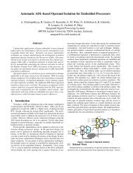
2.4.1 The Boundary-Scan<br />
The boundary-scan test architecture provides means to test interconnects<br />
between integrated circuits on a board without using<br />
physical test probes. It adds a boundary-scan cell that includes<br />
multiplexers <strong>and</strong> latches to each pin on the device (figure<br />
1). A detailed description <strong>of</strong> a boundary scan cell can be<br />
found in [21]. For a <strong>JTAG</strong> implementation, according to the<br />
IEEE st<strong>and</strong>ard, the integration <strong>of</strong> a boundary scan using pad<br />
cells is m<strong>and</strong>atory.<br />
3.1 Processor Core Structure<br />
The following three terms will be referred to:<br />
Entities model the hierarchical structure <strong>of</strong> the architecture.<br />
Every entity is implemented as an entity (VHDL) or a module<br />
(Verilog) on RTL.<br />
A unit implements a cohesive functional block. It is defined<br />
by its purpose, its input <strong>and</strong> output. A unit is implemented as<br />
one or several processes (VHDL) or always blocks (Verilog).<br />
A path establishes links between units. Paths contain<br />
one or more signals. For instance, a write path contains<br />
a signal for enabling the access, a signal propagating the<br />
data <strong>and</strong> a signal transmitting the address (in case <strong>of</strong> an<br />
array access). By using paths, signals can be established,<br />
that transmit information over the boundary <strong>of</strong> an entity.<br />
The signals contained in paths are represented on RTL<br />
as signals <strong>and</strong> ports (VHDL) or regs/wires <strong>and</strong> ports (Verilog).<br />
Figure 1. <strong>JTAG</strong> <strong>Interface</strong> <strong>and</strong> Boundary-Scan<br />
2.4.2 The Test Access Port<br />
The Test Access Port (TAP) is a five pin (TCK, TMS, TRST,<br />
TDI, TDO) general purpose port, which can be used to access<br />
additional functionality <strong>of</strong> the chip (e.g. the boundary scan<br />
chain). Data is propagated serially via TDI towards TDO into<br />
<strong>and</strong> out <strong>of</strong> the architecture. A detailed description <strong>of</strong> the ports<br />
<strong>and</strong> their purpose can be found in [21]. The TAP controller is<br />
the major component <strong>of</strong> a <strong>JTAG</strong> interface. Its functionality is<br />
well defined <strong>and</strong> not subject <strong>of</strong> our investigations.<br />
In order to provide access to vendor-defined functionality<br />
via the <strong>JTAG</strong> interface, it is possible to connect special registers,<br />
the so called test data registers, serially between TDI <strong>and</strong><br />
TDO. The TAP controller selects the current connected register.<br />
Not only a test data register may be selected, but also the<br />
boundary scan chain as shown in figure 1.<br />
3 Extensions to the Processor Core<br />
This section describes required changes to the synthesized<br />
processor core in order to support debugging functionality.<br />
The LISA model description does not have to be modified<br />
to include the debug mechanism. Configurations for this feature<br />
are applied via a Graphical User <strong>Interface</strong> (GUI), which<br />
guides the complete synthesis process.<br />
The general structure <strong>of</strong> a processor core generated from<br />
a LISA processor description is briefly introduced, before the<br />
changes are explained in detail.<br />
Figure 2. Example Architecture Structure<br />
An example entity structure is shown in figure 2. Entities<br />
are represented as rectangles, units as round-cornered boxes<br />
<strong>and</strong> paths as arrows. For simplicity, only the pipeline controller<br />
unit is shown here as a representative unit.<br />
Regarding the different components synthesized from<br />
LISA, the user registers, memories <strong>and</strong> pipeline registers are<br />
affected when generating the debug mechanism (indicated by<br />
the gray color in figure 2). These are the elements, which store<br />
the current processor state <strong>and</strong> thus must be accessible by the<br />
debug mechanism in two ways. On the one h<strong>and</strong>, the processor<br />
has to be halted in debug mode. Therefore, any write access to<br />
storage elements <strong>of</strong> the core has to be blocked. On the other<br />
h<strong>and</strong>, read <strong>and</strong> write access to these elements are necessary to<br />
determine <strong>and</strong> manipulate the state <strong>of</strong> the core.<br />
Required changes to the storage elements <strong>of</strong> the core,<br />
namely user registers, pipeline registers <strong>and</strong> memories are discussed<br />
in the following subsections.<br />
3.2 Registers with <strong>Debug</strong> Support<br />
The structure <strong>of</strong> the register implementation is depicted in<br />
figure 3. This schematic describes the fundamental principle<br />
<strong>of</strong> the general register access <strong>and</strong> the debug functionality. In<br />
this example, we are assuming n read <strong>and</strong> write paths to a register<br />
file with m elements. The white boxes illustrate the regular<br />
processes required for the register implementation. The
write paths coming from functional units are routed to the particular<br />
element <strong>of</strong> the register file via a cross-connect. The<br />
synchronous register implementation leads to the read crossconnect,<br />
which routes the register values to the read paths.<br />
signaled via the breakpoint detection path. In order to detect a<br />
breakpoint correctly, the write enable also has to be taken into<br />
account, such that the breakpoint is only hit if the value has<br />
just been written. If the breakpoint is not value sensitive, the<br />
write enable is the only signal evaluated for the detection.<br />
3.3 Pipeline Registers with <strong>Debug</strong> Support<br />
The modifications to the pipeline register implementation<br />
in order to support debug functionality are very similar to<br />
those for user registers. The implementation only differs, because<br />
stalls <strong>and</strong> flushes have to be treated properly. A detailed<br />
discussion is omitted here, since this difference is not<br />
important for the implementation changes resulting from debug<br />
functionality.<br />
3.4 Memories with <strong>Debug</strong> Support<br />
Figure 3. Register Implementation<br />
The additional gray boxes are only necessary for the implementation<br />
<strong>of</strong> debug functionality. Those represent processes<br />
for setting a register value, reading a register value <strong>and</strong> detecting<br />
breakpoints. Additional paths are shown as dotted arrows.<br />
The debug write process takes care <strong>of</strong> two functionalities<br />
required for debugging. First, it blocks the enable signals<br />
whenever the register enable is inactive. As a result, the register<br />
does not change its value anymore. The register enable<br />
path is a general path indicating whether the processor is<br />
halted <strong>and</strong> therefore has to maintain its current state. Similar<br />
functionality is implemented for all other storage elements <strong>of</strong><br />
the architecture. Thus, it is possible to halt the complete core<br />
in its current state by setting the register enable inactive. Second,<br />
the register value can be overwritten by the debug write<br />
process. The value to be written <strong>and</strong> the according control<br />
signals are provided via debug write paths.<br />
Through the debug read process the current register values<br />
are propagated via debug read paths. Note, that the debug read<br />
<strong>and</strong> write access is only generated for those register elements,<br />
which were configured with the GUI to provide this access. In<br />
figure 3, this is done for only two elements.<br />
The detection <strong>of</strong> breakpoints is also only applied for registers<br />
selected with the GUI. Hardware breakpoints are divided<br />
into program <strong>and</strong> data breakpoints. Whenever a breakpoint is<br />
hit, the processor core is switched to debug mode.<br />
Program breakpoints (sometimes also denoted as instruction<br />
breakpoints) are activated before the instruction associated<br />
with a pre-selected address, changes the state <strong>of</strong> the architecture.<br />
Thus, they are related to the program counter register.<br />
Data breakpoints are related to any other user register. A data<br />
breakpoint is activated when the selected user register is written<br />
to. Moreover, data breakpoints may be value sensitive.<br />
This means the breakpoint is activated only if a certain predefined<br />
value is written.<br />
In the breakpoint detection process, the register value is compared<br />
with the according breakpoint value provided via breakpoint<br />
control paths. In case <strong>of</strong> a match, the breakpoint hit is<br />
The general idea <strong>of</strong> accessing memories in debug mode is<br />
equivalent to the mechanism for registers. The basic difference<br />
is, that in the case <strong>of</strong> register implementation the debug<br />
access can be included directly into the register implementation.<br />
Memories, being inseparable basic blocks with a limited<br />
number <strong>of</strong> ports, do not allow an embedded generation <strong>of</strong> debug<br />
mechanism like registers. Thus, the default read <strong>and</strong> write<br />
ports have to be used for debug access.<br />
Figure 4. Memory Implementation<br />
Figure 4 shows an example <strong>of</strong> a memory with one dedicated<br />
read <strong>and</strong> one dedicated write port. There are n write<br />
<strong>and</strong> m read paths connected to the memory. They are mapped<br />
to the existing memory ports in the access mapping process.<br />
The gray illustrated debug access process is used in two ways.<br />
By evaluating the register enable signal write accesses can be<br />
blocked in debug mode. This is necessary in order to maintain<br />
the current processor state. Additionally, the process bypasses<br />
a debug read <strong>and</strong> write access during debug mode.<br />
3.5 Effort Estimation<br />
As shown in the previous sections, the effort for changing<br />
the core implementation on RTL manually in order to support<br />
debug features cannot be neglected. Especially, an exploration<br />
<strong>of</strong> different configurations <strong>of</strong> debug functionality would be<br />
very time consuming, if changes to the register implementation<br />
<strong>and</strong> the implementation <strong>of</strong> access mapping for memories<br />
would have to be applied manually.
4 <strong>JTAG</strong> <strong>Interface</strong> <strong>Generation</strong><br />
We developed a debug mechanism, suited to architectures<br />
<strong>of</strong> various domains. Its features are accessed by sending<br />
debugging instructions through the <strong>JTAG</strong> interface. The<br />
st<strong>and</strong>ard compliant way to establish test features, which<br />
are accessible via the <strong>JTAG</strong> interface, makes use <strong>of</strong> vendor<br />
defined test data registers.<br />
Figure 5. Extended Model Structure with <strong>Debug</strong><br />
<strong>Mechanism</strong><br />
As shown in figure 5, the architecture entity is embedded in<br />
the top level entity, where the TAP controller <strong>and</strong> the test data<br />
register is also placed. In order to control the automatically<br />
generated debug mechanism, one test data register is instantiated.<br />
The generated <strong>JTAG</strong> interface <strong>and</strong> debug mechanism<br />
communicates (only) through this single register. Thus, the<br />
debug mechanism can also be generated without <strong>JTAG</strong> interface.<br />
In this case, the control <strong>of</strong> the debug interface is up to the<br />
designer. Due to this concept, our approach is highly flexible.<br />
The test data register is the connection between the <strong>JTAG</strong><br />
interface <strong>and</strong> the debug mechanism. A direct connection <strong>of</strong><br />
the paths resulting from the core modifications to a test data<br />
register is hardly possible. Thus, special units have to be introduced<br />
in order to support debug functionality (debug state<br />
machine <strong>and</strong> mode control). They are connected between the<br />
test data register <strong>and</strong> the modified processor core. A detailed<br />
description is included in the next section.<br />
The TAP controller writes the test data debug register serially<br />
in order to control the debug mechanism. Data, which is<br />
written, is stored left most in the register <strong>and</strong> data to be read is<br />
stored right most. By this, unnecessary shifting <strong>of</strong> the register<br />
is avoided. The TAP controller unit is mapped to a Design-<br />
Ware component [22] during the synthesis process.<br />
Our ASIP generation targets complex System-on-Chip<br />
(SoC) designs <strong>and</strong> the generated ASIP is only one part <strong>of</strong> the<br />
whole system. Thus, we are not dealing directly with pad cells.<br />
It is up to the designer to complete the implementation according<br />
to these requirements.<br />
5 <strong>Debug</strong> <strong>Mechanism</strong> <strong>Generation</strong><br />
In figure 5, the additional units required to implement the<br />
debug mechanism are also shown.<br />
The debug state machine accesses the test data debug register.<br />
It receives data words (like instructions, P1) <strong>and</strong> writes<br />
out the requested data words (such as a register value which<br />
has been read, P2) parallel. The debug state machine is the<br />
central element which implements the core functionality <strong>of</strong> the<br />
whole debug mechanism. It decodes <strong>and</strong> executes the debug<br />
instructions. Whenever requested data is stored in the test data<br />
debug register, it is indicated via the additional pin RDY RD.<br />
This is required to establish a reasonable fast communication<br />
through the <strong>JTAG</strong> interface, since the interface itself is passive<br />
<strong>and</strong> not able to indicate events itself. The debug state machine<br />
is connected to the architecture with several paths as shown in<br />
figure 5 (P3). Via these paths, registers can be accessed (debug<br />
read <strong>and</strong> write paths) <strong>and</strong> breakpoint values are provided<br />
(breakpoint control paths). The mapping <strong>of</strong> the debug state<br />
machine unit to processes during the synthesis is strongly influenced<br />
by the configuration <strong>of</strong> the debug mechanism given<br />
via the GUI.<br />
The mode control is a state machine to change the processor<br />
core from user mode to debug mode. The paths between<br />
the mode control <strong>and</strong> the debug state machine (P4) are used<br />
to indicate the current mode <strong>and</strong> to transmit mode changing<br />
instructions (e.g. single cycle execution) to the mode control<br />
unit. Two additional pins are directly connected to the mode<br />
control: DBG REQ is dedicated to switch the processor to debug<br />
mode via interrupt; DBG MD indicates the current mode<br />
<strong>of</strong> the processor to the outside. The paths connecting the mode<br />
control <strong>and</strong> the architecture (P5) are used to notify breakpoint<br />
hits (breakpoint detection paths) <strong>and</strong> to indicate a required halt<br />
<strong>of</strong> the processor (register enable path).<br />
6 Results<br />
The impact <strong>of</strong> a debug mechanism to the gate level synthesis<br />
results, such as clock speed <strong>and</strong> area, are discussed in this<br />
section.<br />
The sample architecture is derived from the Motorola 6811 architecture<br />
[23]. This pipelined architecture with three pipeline<br />
stages <strong>and</strong> 16/32 bit instruction word is assembly compatible<br />
to the original architecture. All syntheses were done using a<br />
0.18 µm technology. The area without debug mechanism (table<br />
1, run 1) is 31.6 kGates, whereas an implementation with<br />
full debug support (table 1, run 2) takes 45.6 kGates. This is<br />
an increase <strong>of</strong> 44%. Full debug support means, that each <strong>of</strong><br />
the 26 user registers can be written/ read while the processor<br />
is in debug mode <strong>and</strong> one breakpoint can be set to every register.<br />
Additionally, four program breakpoints can be set.<br />
By analyzing the results, the major portion <strong>of</strong> area overhead<br />
is caused by the state machine <strong>and</strong> the extended register implementation<br />
according to section 3 <strong>and</strong> 5. The main area increase<br />
results from the fact, that breakpoints are implemented<br />
independently for each register <strong>and</strong> thereby introduce additional<br />
flipflops <strong>and</strong> comparators for each register.<br />
Only five <strong>of</strong> the 26 registers are accessible directly using assembler<br />
instructions. The others are used for internal purposes
(e.g. for the state machine for division instructions). Thus,<br />
data breakpoints related to these registers are not required.<br />
Consequently, in a third synthesis (table 1, run 3), we only<br />
added breakpoints <strong>and</strong> debug access to the five main registers.<br />
With this reasonably reduced amount <strong>of</strong> debug capabilities<br />
the required chip area for the complete architecture takes<br />
36.4 kGates. This is only an increase <strong>of</strong> 15 % compared to<br />
the area used for the architecture without debug interface. The<br />
slight decrease <strong>of</strong> area consumption for the pipeline results<br />
from dynamic optimization criteria <strong>of</strong> the synthesis tool <strong>and</strong><br />
range within its accuracy.<br />
area (kGates)<br />
run 1 run 2 run 3<br />
architecture no debug full debug reduced debug<br />
part capabilities capabilities capabilities<br />
total 31.6 100% 45.6 144% 36.4 115%<br />
pipeline 20.4 100% 20.4 100% 19.7 97%<br />
register file 11.1 100% 15.9 143% 12.1 109%<br />
debug SM - 7.7 3.1<br />
mode control - 0.2 0.2<br />
test-data-reg - 0.6 0.6<br />
TAP controller - 0.6 0.6<br />
Table 1. Area Consumption for Three Configurations<br />
<strong>of</strong> the M68HC11<br />
The implementation has been chosen in such a way that,<br />
potential critical paths are least affected. However, as can be<br />
seen in section 5 the debug-write features could not be fully<br />
removed from this critical path. Thus, there is a theoretical<br />
influence on the timing. Nevertheless, for this case study the<br />
deviations concerning timing range within the accuracy <strong>of</strong> the<br />
gate level synthesis tool. The data arrival time <strong>of</strong> the critical<br />
path amounted to about 4.5 ns. Thus, the values <strong>of</strong> the resulting<br />
maximum frequencies all are located in the range from 215<br />
MHz to 225 MHz.<br />
7 Conclusion <strong>and</strong> Future Work<br />
In this paper we presented the first automatic generation<br />
<strong>of</strong> a <strong>JTAG</strong> interface <strong>and</strong> debug mechanism from an ADL. This<br />
generation is embedded into our RTL processor synthesis flow,<br />
which uses the language LISA to generate an RTL representation<br />
<strong>of</strong> the architecture. The <strong>JTAG</strong> interface is used as interface<br />
to the architecture <strong>and</strong> thus to the debug mechanism.<br />
The debug mechanism enables features like program <strong>and</strong> data<br />
breakpoints or register read <strong>and</strong> write access. The presented<br />
synthesis results clarified that debugging capabilities should<br />
be chosen judiciously, as they have a major effect on the chip<br />
area <strong>of</strong> the target architecture. Using our RTL processor synthesis<br />
tool, the designer is able to perform this selection during<br />
design space exploration.<br />
In our future work we will investigate the suitability <strong>of</strong> our<br />
debug mechanism for architectures <strong>of</strong> various domains. Moreover,<br />
the results showed, that the current breakpoint implementation<br />
has a major impact on the required area consumption.<br />
Different improvements to the current implementation <strong>of</strong><br />
breakpoints are being investigated. Their implementation will<br />
be addressed in our future work.<br />
References<br />
[1] G. Hadjiyiannis <strong>and</strong> S. Devadas. Techniques for Accurate Performance<br />
Evaluation in Architecture Exploration. IEEE Transactions on VLSI<br />
Systems, 2002.<br />
[2] P. Mishra, A. Kejariwal, <strong>and</strong> N. Dutt. Rapid Exploration <strong>of</strong> Pipelined<br />
Processors through <strong>Automatic</strong> <strong>Generation</strong> <strong>of</strong> Synthesizable RTL Models<br />
Rapid System Prototyping. Workshop on Rapid System Prototyping<br />
(RSP), 2003.<br />
[3] V. Rajesh <strong>and</strong> R. Moona. Processor Modeling for Hardware S<strong>of</strong>tware<br />
Codesign. In Int. Conf. on VLSI Design, Jan. 1999.<br />
[4] O. Schliebusch, A. H<strong>of</strong>fmann, A. Nohl, G. Braun, <strong>and</strong> H. Meyr. Architecture<br />
Implementation Using the Machine Description Language LISA.<br />
In Proc. <strong>of</strong> the ASPDAC/VLSI Design - Bangalore, India, Jan. 2002.<br />
[5] Schliebusch, O. <strong>and</strong> Chattopadhyay, A. <strong>and</strong> Steinert, M. <strong>and</strong> Braun, G.<br />
<strong>and</strong> Nohl, A. <strong>and</strong> Leupers, R. <strong>and</strong> Ascheid, G. <strong>and</strong> Meyr, H. RTL Processor<br />
Synthesis for Architecture Exploration <strong>and</strong> Implementation. In<br />
Proceedings <strong>of</strong> the Conference on Design, Automation & Test in Europe<br />
(DATE) - Designers Forum, Paris, France, Feb 2004.<br />
[6] A. H<strong>of</strong>fmann, H. Meyr, <strong>and</strong> R. Leupers. Architecture Exploration for<br />
Embedded Processors with LISA. Kluwer Academic Publishers, 2002.<br />
[7] M. Steinert, O. Schliebusch, <strong>and</strong> O. Zerres. Design Flow for Processor<br />
Development using SystemC. In SNUG Europe Proceedings - Munich,<br />
Germany, Mar. 2003.<br />
[8] H. Scharwaechter, D. Kammler, A. Wieferink, M. Hohenauer, J. Zeng,<br />
K. Karuri, R. Leupers, G. Ascheid, <strong>and</strong> H. Meyr. ASIP Architecture<br />
Exploration for Efficient IPSec Encryption: A Case Study. In Proc.<br />
<strong>of</strong> the Workshop on S<strong>of</strong>tware <strong>and</strong> Compilers for Embedded Systems<br />
(SCOPES), Sep. 2004.<br />
[9] G. Hadjiyiannis <strong>and</strong> S. Hanono <strong>and</strong> S. Devadas. ISDL: An Instruction<br />
Set Description Language for Retargetability. In Proc. <strong>of</strong> the Design<br />
Automation Conference (DAC), Jun. 1997.<br />
[10] A. Fauth <strong>and</strong> J. Van Praet <strong>and</strong> M. Freericks. Describing Instruction<br />
Set Processors Using nML. In Proc. <strong>of</strong> the European Design <strong>and</strong> Test<br />
Conference (ED&TC), Mar. 1995.<br />
[11] Target Compiler Technologies. http://www.retarget.com.<br />
[12] A. Halambi <strong>and</strong> P. Grun <strong>and</strong> V. Ganesh <strong>and</strong> A. Khare <strong>and</strong> N. Dutt <strong>and</strong><br />
A. Nicolau. EXPRESSION: A Language for Architecture Exploration<br />
through Compiler/Simulator Retargetability. In Proc. <strong>of</strong> the Conference<br />
on Design, Automation & Test in Europe (DATE), Mar. 1999.<br />
[13] P. Paulin <strong>and</strong> C. Liem <strong>and</strong> T.C. May <strong>and</strong> S. Sutarwala. FlexWare: A<br />
Flexible Firmware Development Environment for Embedded Systems.<br />
In P. Marwedel <strong>and</strong> G. Goosens, editors, Code <strong>Generation</strong> for Embedded<br />
Processors. Kluwer Academic Publishers, 1995.<br />
[14] A. Kitajima <strong>and</strong> M. Itoh <strong>and</strong> J. Sato <strong>and</strong> A. Shiomi <strong>and</strong> Y. Takeuchi <strong>and</strong><br />
M. Imai. Effectiveness <strong>of</strong> the ASIP Design System PEAS-III in Design<br />
<strong>of</strong> Pipelined Processors. In Proc. <strong>of</strong> the Asia South Pacific Design<br />
Automation Conference (ASPDAC), Jan. 2001.<br />
[15] ASIP Meister. http://www.eda-meister.org.<br />
[16] R. Gonzales. Xtensa: A configurable <strong>and</strong> extensible processor. IEEE<br />
Micro, Mar. 2000.<br />
[17] Tensilica. http://www.tensilica.com.<br />
[18] Stretch. http://www.stretchinc.com.<br />
[19] V. Kathail <strong>and</strong> S. Aditya <strong>and</strong> R. Schreiber <strong>and</strong> B.R. Rau <strong>and</strong> D. Cronquist<br />
<strong>and</strong> M. Sivaraman. <strong>Automatic</strong>ally Designing Custom Computers.<br />
IEEE Computer, 35(9):39–47, Sept. 2002.<br />
[20] IEEE-ISTO. The Nexus 5001 Forum, St<strong>and</strong>ard for a Global Embedded<br />
Processor <strong>Debug</strong> <strong>Interface</strong>, December 1999.<br />
[21] IEEE, Inc., 3 Park Avenue, New York, NY 10016-5997, USA. IEEE Std<br />
1149.1-2001, St<strong>and</strong>ard Test Access Port <strong>and</strong> Boundary-Scan Architecture,<br />
June 2001.<br />
[22] Synopsys. DesignWare Components<br />
http://www.synopsys.com/products/designware/designware.html.<br />
[23] Motorola. 68HC11: Microcontroller<br />
http://www.motorola.com.