Automatic Generation of JTAG Interface and Debug Mechanism - ICE
Automatic Generation of JTAG Interface and Debug Mechanism - ICE
Automatic Generation of JTAG Interface and Debug Mechanism - ICE

Create successful ePaper yourself
Turn your PDF publications into a flip-book with our unique Google optimized e-Paper software.
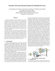
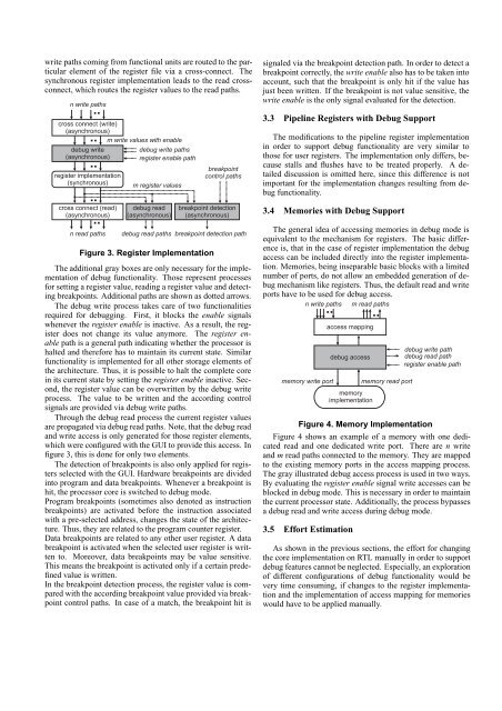
write paths coming from functional units are routed to the particular<br />
element <strong>of</strong> the register file via a cross-connect. The<br />
synchronous register implementation leads to the read crossconnect,<br />
which routes the register values to the read paths.<br />
signaled via the breakpoint detection path. In order to detect a<br />
breakpoint correctly, the write enable also has to be taken into<br />
account, such that the breakpoint is only hit if the value has<br />
just been written. If the breakpoint is not value sensitive, the<br />
write enable is the only signal evaluated for the detection.<br />
3.3 Pipeline Registers with <strong>Debug</strong> Support<br />
The modifications to the pipeline register implementation<br />
in order to support debug functionality are very similar to<br />
those for user registers. The implementation only differs, because<br />
stalls <strong>and</strong> flushes have to be treated properly. A detailed<br />
discussion is omitted here, since this difference is not<br />
important for the implementation changes resulting from debug<br />
functionality.<br />
3.4 Memories with <strong>Debug</strong> Support<br />
Figure 3. Register Implementation<br />
The additional gray boxes are only necessary for the implementation<br />
<strong>of</strong> debug functionality. Those represent processes<br />
for setting a register value, reading a register value <strong>and</strong> detecting<br />
breakpoints. Additional paths are shown as dotted arrows.<br />
The debug write process takes care <strong>of</strong> two functionalities<br />
required for debugging. First, it blocks the enable signals<br />
whenever the register enable is inactive. As a result, the register<br />
does not change its value anymore. The register enable<br />
path is a general path indicating whether the processor is<br />
halted <strong>and</strong> therefore has to maintain its current state. Similar<br />
functionality is implemented for all other storage elements <strong>of</strong><br />
the architecture. Thus, it is possible to halt the complete core<br />
in its current state by setting the register enable inactive. Second,<br />
the register value can be overwritten by the debug write<br />
process. The value to be written <strong>and</strong> the according control<br />
signals are provided via debug write paths.<br />
Through the debug read process the current register values<br />
are propagated via debug read paths. Note, that the debug read<br />
<strong>and</strong> write access is only generated for those register elements,<br />
which were configured with the GUI to provide this access. In<br />
figure 3, this is done for only two elements.<br />
The detection <strong>of</strong> breakpoints is also only applied for registers<br />
selected with the GUI. Hardware breakpoints are divided<br />
into program <strong>and</strong> data breakpoints. Whenever a breakpoint is<br />
hit, the processor core is switched to debug mode.<br />
Program breakpoints (sometimes also denoted as instruction<br />
breakpoints) are activated before the instruction associated<br />
with a pre-selected address, changes the state <strong>of</strong> the architecture.<br />
Thus, they are related to the program counter register.<br />
Data breakpoints are related to any other user register. A data<br />
breakpoint is activated when the selected user register is written<br />
to. Moreover, data breakpoints may be value sensitive.<br />
This means the breakpoint is activated only if a certain predefined<br />
value is written.<br />
In the breakpoint detection process, the register value is compared<br />
with the according breakpoint value provided via breakpoint<br />
control paths. In case <strong>of</strong> a match, the breakpoint hit is<br />
The general idea <strong>of</strong> accessing memories in debug mode is<br />
equivalent to the mechanism for registers. The basic difference<br />
is, that in the case <strong>of</strong> register implementation the debug<br />
access can be included directly into the register implementation.<br />
Memories, being inseparable basic blocks with a limited<br />
number <strong>of</strong> ports, do not allow an embedded generation <strong>of</strong> debug<br />
mechanism like registers. Thus, the default read <strong>and</strong> write<br />
ports have to be used for debug access.<br />
Figure 4. Memory Implementation<br />
Figure 4 shows an example <strong>of</strong> a memory with one dedicated<br />
read <strong>and</strong> one dedicated write port. There are n write<br />
<strong>and</strong> m read paths connected to the memory. They are mapped<br />
to the existing memory ports in the access mapping process.<br />
The gray illustrated debug access process is used in two ways.<br />
By evaluating the register enable signal write accesses can be<br />
blocked in debug mode. This is necessary in order to maintain<br />
the current processor state. Additionally, the process bypasses<br />
a debug read <strong>and</strong> write access during debug mode.<br />
3.5 Effort Estimation<br />
As shown in the previous sections, the effort for changing<br />
the core implementation on RTL manually in order to support<br />
debug features cannot be neglected. Especially, an exploration<br />
<strong>of</strong> different configurations <strong>of</strong> debug functionality would be<br />
very time consuming, if changes to the register implementation<br />
<strong>and</strong> the implementation <strong>of</strong> access mapping for memories<br />
would have to be applied manually.