Automatic Generation of JTAG Interface and Debug Mechanism - ICE
Automatic Generation of JTAG Interface and Debug Mechanism - ICE
Automatic Generation of JTAG Interface and Debug Mechanism - ICE

You also want an ePaper? Increase the reach of your titles
YUMPU automatically turns print PDFs into web optimized ePapers that Google loves.
4 <strong>JTAG</strong> <strong>Interface</strong> <strong>Generation</strong><br />
We developed a debug mechanism, suited to architectures<br />
<strong>of</strong> various domains. Its features are accessed by sending<br />
debugging instructions through the <strong>JTAG</strong> interface. The<br />
st<strong>and</strong>ard compliant way to establish test features, which<br />
are accessible via the <strong>JTAG</strong> interface, makes use <strong>of</strong> vendor<br />
defined test data registers.<br />
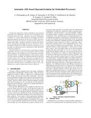
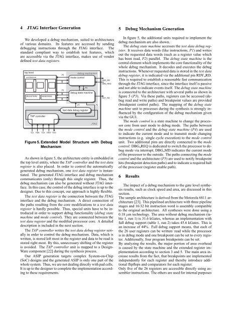
Figure 5. Extended Model Structure with <strong>Debug</strong><br />
<strong>Mechanism</strong><br />
As shown in figure 5, the architecture entity is embedded in<br />
the top level entity, where the TAP controller <strong>and</strong> the test data<br />
register is also placed. In order to control the automatically<br />
generated debug mechanism, one test data register is instantiated.<br />
The generated <strong>JTAG</strong> interface <strong>and</strong> debug mechanism<br />
communicates (only) through this single register. Thus, the<br />
debug mechanism can also be generated without <strong>JTAG</strong> interface.<br />
In this case, the control <strong>of</strong> the debug interface is up to the<br />
designer. Due to this concept, our approach is highly flexible.<br />
The test data register is the connection between the <strong>JTAG</strong><br />
interface <strong>and</strong> the debug mechanism. A direct connection <strong>of</strong><br />
the paths resulting from the core modifications to a test data<br />
register is hardly possible. Thus, special units have to be introduced<br />
in order to support debug functionality (debug state<br />
machine <strong>and</strong> mode control). They are connected between the<br />
test data register <strong>and</strong> the modified processor core. A detailed<br />
description is included in the next section.<br />
The TAP controller writes the test data debug register serially<br />
in order to control the debug mechanism. Data, which is<br />
written, is stored left most in the register <strong>and</strong> data to be read is<br />
stored right most. By this, unnecessary shifting <strong>of</strong> the register<br />
is avoided. The TAP controller unit is mapped to a Design-<br />
Ware component [22] during the synthesis process.<br />
Our ASIP generation targets complex System-on-Chip<br />
(SoC) designs <strong>and</strong> the generated ASIP is only one part <strong>of</strong> the<br />
whole system. Thus, we are not dealing directly with pad cells.<br />
It is up to the designer to complete the implementation according<br />
to these requirements.<br />
5 <strong>Debug</strong> <strong>Mechanism</strong> <strong>Generation</strong><br />
In figure 5, the additional units required to implement the<br />
debug mechanism are also shown.<br />
The debug state machine accesses the test data debug register.<br />
It receives data words (like instructions, P1) <strong>and</strong> writes<br />
out the requested data words (such as a register value which<br />
has been read, P2) parallel. The debug state machine is the<br />
central element which implements the core functionality <strong>of</strong> the<br />
whole debug mechanism. It decodes <strong>and</strong> executes the debug<br />
instructions. Whenever requested data is stored in the test data<br />
debug register, it is indicated via the additional pin RDY RD.<br />
This is required to establish a reasonable fast communication<br />
through the <strong>JTAG</strong> interface, since the interface itself is passive<br />
<strong>and</strong> not able to indicate events itself. The debug state machine<br />
is connected to the architecture with several paths as shown in<br />
figure 5 (P3). Via these paths, registers can be accessed (debug<br />
read <strong>and</strong> write paths) <strong>and</strong> breakpoint values are provided<br />
(breakpoint control paths). The mapping <strong>of</strong> the debug state<br />
machine unit to processes during the synthesis is strongly influenced<br />
by the configuration <strong>of</strong> the debug mechanism given<br />
via the GUI.<br />
The mode control is a state machine to change the processor<br />
core from user mode to debug mode. The paths between<br />
the mode control <strong>and</strong> the debug state machine (P4) are used<br />
to indicate the current mode <strong>and</strong> to transmit mode changing<br />
instructions (e.g. single cycle execution) to the mode control<br />
unit. Two additional pins are directly connected to the mode<br />
control: DBG REQ is dedicated to switch the processor to debug<br />
mode via interrupt; DBG MD indicates the current mode<br />
<strong>of</strong> the processor to the outside. The paths connecting the mode<br />
control <strong>and</strong> the architecture (P5) are used to notify breakpoint<br />
hits (breakpoint detection paths) <strong>and</strong> to indicate a required halt<br />
<strong>of</strong> the processor (register enable path).<br />
6 Results<br />
The impact <strong>of</strong> a debug mechanism to the gate level synthesis<br />
results, such as clock speed <strong>and</strong> area, are discussed in this<br />
section.<br />
The sample architecture is derived from the Motorola 6811 architecture<br />
[23]. This pipelined architecture with three pipeline<br />
stages <strong>and</strong> 16/32 bit instruction word is assembly compatible<br />
to the original architecture. All syntheses were done using a<br />
0.18 µm technology. The area without debug mechanism (table<br />
1, run 1) is 31.6 kGates, whereas an implementation with<br />
full debug support (table 1, run 2) takes 45.6 kGates. This is<br />
an increase <strong>of</strong> 44%. Full debug support means, that each <strong>of</strong><br />
the 26 user registers can be written/ read while the processor<br />
is in debug mode <strong>and</strong> one breakpoint can be set to every register.<br />
Additionally, four program breakpoints can be set.<br />
By analyzing the results, the major portion <strong>of</strong> area overhead<br />
is caused by the state machine <strong>and</strong> the extended register implementation<br />
according to section 3 <strong>and</strong> 5. The main area increase<br />
results from the fact, that breakpoints are implemented<br />
independently for each register <strong>and</strong> thereby introduce additional<br />
flipflops <strong>and</strong> comparators for each register.<br />
Only five <strong>of</strong> the 26 registers are accessible directly using assembler<br />
instructions. The others are used for internal purposes