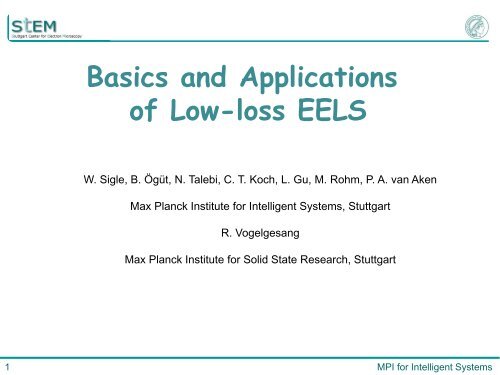
Basics and applications of low-loss EELS
Basics and applications of low-loss EELS
Basics and applications of low-loss EELS

You also want an ePaper? Increase the reach of your titles
YUMPU automatically turns print PDFs into web optimized ePapers that Google loves.
<strong>Basics</strong> <strong>and</strong> Applications<br />
<strong>of</strong> Low-<strong>loss</strong> <strong>EELS</strong><br />
W. Sigle, B. Ögüt, N. Talebi, C. T. Koch, L. Gu, M. Rohm, P. A. van Aken<br />
Max Planck Institute for Intelligent Systems, Stuttgart<br />
R. Vogelgesang<br />
Max Planck Institute for Solid State Research, Stuttgart<br />
1<br />
MPI for Intelligent Systems
Outline<br />
I. Dielectric formulation<br />
II.<br />
III.<br />
IV.<br />
Low-<strong>loss</strong> mechanisms in bulk <strong>and</strong> finite media<br />
Instrumentation <strong>and</strong> methods<br />
Applications<br />
2<br />
MPI for Intelligent Systems
The energy-<strong>loss</strong> process<br />
+<br />
+<br />
+<br />
-<br />
-<br />
-<br />
Electron probes<br />
z-component<br />
<strong>of</strong> electric field<br />
Path<br />
3<br />
Energy <strong>loss</strong>:<br />
<br />
Path<br />
<br />
E ( r,<br />
t)<br />
dt<br />
v – electron velocity<br />
t - time<br />
MPI for Intelligent Systems
The dielectric function<br />
Polarizability<br />
Absorption<br />
Dielectric function<br />
<br />
( 2<br />
)<br />
1(<br />
)<br />
i<br />
( )<br />
describes the response <strong>of</strong> a<br />
material to an applied field<br />
<br />
MPI for Intelligent Systems
Dielectric formulation <strong>of</strong> energy <strong>loss</strong><br />
S(<br />
E)<br />
Single<br />
scattering<br />
distribution<br />
<br />
2 I0 t<br />
b<br />
Im( 1/ (<br />
E))<br />
2<br />
ln1<br />
( )<br />
a m v<br />
qE<br />
0<br />
0<br />
Normalization <strong>and</strong><br />
sample thickness<br />
Energy <strong>loss</strong><br />
function<br />
2<br />
<br />
<br />
<br />
Angular scattering<br />
distribution<br />
m o – Electron rest mass<br />
a o – Bohr radius ≈ 0.0529 nm<br />
b – Collection angle<br />
q E ≈ DE/2E o<br />
The <strong>EELS</strong> spectrum contains the full information about the<br />
dielectric function, including optical properties <strong>of</strong> the material.<br />
5<br />
MPI for Intelligent Systems
The energy-<strong>loss</strong> function<br />
Im( <br />
1<br />
)<br />
<br />
<br />
<br />
2<br />
1<br />
2<br />
<br />
2<br />
2<br />
Maxima:<br />
2 small, 1 close to zero Plasmon (collective excitation)<br />
2 small, 1 close to 1 Im(-1/)= 2 Interb<strong>and</strong> transition<br />
(single-electron excitation)<br />
6<br />
MPI for Intelligent Systems
The energy-<strong>loss</strong> function<br />
Example: Al<br />
3<br />
2<br />
1<br />
0<br />
Eps1<br />
Eps2<br />
ELF<br />
-1<br />
-2<br />
5 7 9 11 13 15 17 19<br />
Energy (eV)<br />
7<br />
MPI for Intelligent Systems
4<br />
The energy-<strong>loss</strong> function<br />
Volume plasmon<br />
Example: Ag<br />
dsp interb<strong>and</strong> transitions<br />
(+ plasmon)<br />
Surface plasmon 3<br />
2<br />
1<br />
Eps1<br />
Eps2<br />
-Im(1/Eps)<br />
-Im(1/(Eps+1))<br />
0<br />
-1<br />
1 3 5 7 9<br />
Energy (eV)<br />
is closely connected with the electronic structure <strong>of</strong> a material<br />
MPI for Intelligent Systems
How to obtain the complex (E) <br />
Input:<br />
Refractive index<br />
=<br />
x<br />
S(<br />
E)<br />
<br />
2 I<br />
t<br />
a m <br />
0<br />
b<br />
Im( 1/ (<br />
E))<br />
ln1<br />
(<br />
qE<br />
0 2<br />
)<br />
2<br />
0<br />
v<br />
<br />
<br />
<br />
9<br />
Courtesy : M. Stöger-Pollach<br />
MPI for Intelligent Systems
Calculation <strong>of</strong> electron scattering from <br />
Specimen<br />
<br />
Momentum transfer q<br />
(scattering angle)<br />
Image plane<br />
g<br />
Energy <strong>loss</strong><br />
DE = ħ ∙ ω<br />
ω-q maps: Raising the specimen<br />
above eucentric position in image<br />
mode with spot illumination<br />
ω-q maps: Dispersion <strong>of</strong> excitations, e.g.<br />
plasmon modes <strong>and</strong> Cerenkov <strong>loss</strong>es<br />
10<br />
MPI for Intelligent Systems
Calculation <strong>of</strong> electron scattering from <br />
E. Kröger, Z. Physik 216, 115 (1968))<br />
Volume <strong>loss</strong> + Cerenkov<br />
Surface plasmons<br />
Guided-light modes<br />
11<br />
MPI for Intelligent Systems
Energy <strong>loss</strong> (eV)<br />
Calculation <strong>of</strong> electron scattering from <br />
Electron <strong>loss</strong> versus scattering angle in Ag<br />
(perpendicular transmission through thin film)<br />
Thickness<br />
Bulk<br />
0<br />
50 nm 100 nm<br />
10<br />
(Max=6·10 6 ) (Max=6·10 6 ) (Max=30)<br />
0 100<br />
µrad<br />
SP coupling<br />
0 100<br />
µrad<br />
No SP coupling<br />
0 100<br />
µrad<br />
12<br />
Relativistic calculation (after E. Kröger, Z. Physik 216, 115 (1968))<br />
MPI for Intelligent Systems
Outline<br />
I. Dielectric formulation<br />
II.<br />
III.<br />
IV.<br />
Low-<strong>loss</strong> mechanisms in bulk <strong>and</strong> finite media<br />
Instrumentation <strong>and</strong> methods<br />
Applications<br />
13<br />
MPI for Intelligent Systems
Valence electron energy <strong>loss</strong>es<br />
Bulk<br />
Interb<strong>and</strong> transition<br />
Volume plasmon<br />
Phonon scattering<br />
Finite media<br />
Surface plasmon<br />
Interface plasmon<br />
Transition radiation<br />
Cerenkov radiation<br />
Guided-light modes<br />
DE< 0.2 eV<br />
Bremsstrahlung<br />
Exciton<br />
14<br />
http://northbeggar.wordpress.com/2009/10/04/exciton/<br />
http://www.j-schoenen.de/abc-manual/a/Strahlung.html<br />
Battacharya et al. , J. Non-Cryst. Sol. (2012)<br />
http://www.kph.uni-mainz.de/243.php MPI for Intelligent Systems
Cerenkov <strong>loss</strong>es<br />
q C<br />
vt<br />
ct/ 1/2<br />
vt<br />
ct/ 1/2<br />
<br />
c<br />
<br />
<br />
c<br />
<br />
15<br />
MPI for Intelligent Systems
Cerenkov <strong>loss</strong><br />
Volume<br />
Interb<strong>and</strong> transition<br />
Cerenkov radiation<br />
(if b 2 >1)<br />
q<br />
Si , 100 keV<br />
P<br />
Volume<br />
plasmon<br />
DE<br />
Simulation (after Kröger 1968)<br />
MPI for Intelligent Systems
efractive index n<br />
Cerenkov <strong>loss</strong><br />
acceleration voltage (kV)<br />
A <strong>low</strong>er acceleration voltage al<strong>low</strong>s higher n materials<br />
to be probed without Cerenkov <strong>loss</strong>es.<br />
17<br />
MPI for Intelligent Systems
Outline<br />
I. Dielectric formulation<br />
II.<br />
III.<br />
IV.<br />
Low-<strong>loss</strong> mechanisms in bulk <strong>and</strong> finite media<br />
Instrumentation <strong>and</strong> methods<br />
Applications<br />
18<br />
MPI for Intelligent Systems
Instrumentation<br />
SESAM<br />
200 kV FEG, HV stability: 2∙10 -7 (rms)<br />
Electrostatic Ω-type monochromator<br />
Extremely stable support frame<br />
with hanging column<br />
2 HAADF detectors<br />
(STEM, EFSTEM)<br />
MANDOLINE energy filter<br />
Filter current stability: 2∙10 -8 (rms)<br />
Plan film camera<br />
with imaging plates,<br />
SSCCD, TV-CCD<br />
Koch et al., Microscopy <strong>and</strong> Microanalysis 12 (2006) 506<br />
19<br />
MPI for Intelligent Systems
Data acquisition<br />
Specimen<br />
STEM<br />
Energy-filtered<br />
imaging<br />
EFTEM<br />
20<br />
MPI for Intelligent Systems
EFTEM versus STEM<br />
EFTEM<br />
STEM<br />
Image sampling + –<br />
Spectral sampling – +<br />
Electron dose high <strong>low</strong><br />
…..STEM <strong>and</strong> EFTEM are complementary<br />
21<br />
MPI for Intelligent Systems
EFTEM versus STEM<br />
Surface plasmon detection with electrons<br />
STEM–<br />
<strong>EELS</strong><br />
J. Nelayah et al., Nature Physics 3 (2007) 348.<br />
ω = 0.9 eV<br />
ω = 1.5 eV<br />
ω = 2.0 eV<br />
EFTEM<br />
100 nm<br />
100 nm 100 nm 100 nm<br />
J. Nelayah et al., Proc.14th EMC (2008) 243.<br />
J. Nelayah et al., Optics Letters 34 (2009) 1003.<br />
STEM <strong>and</strong> EFTEM give qualitatively same results ….<br />
22<br />
MPI for Intelligent Systems
Electron monochromator<br />
Emitter Assembly<br />
Gun Lens<br />
High dispersion<br />
Piezo driven multi slit<br />
Straight beam path (MC <strong>of</strong>f)<br />
Dispersion-free (no rainbow<br />
illumination)<br />
MC<br />
Slit Selector<br />
Dispersive<br />
Plane (Slit)<br />
23<br />
MPI for Intelligent Systems
Energy resolution<br />
VG<br />
VG<br />
Tails <strong>of</strong> zero-<strong>loss</strong> peak are markedly reduced<br />
by use <strong>of</strong> monochromator<br />
24<br />
MPI for Intelligent Systems
Delocalization (nm)<br />
How local is the excitation<br />
Electron probe size (STEM):<br />
0.1 nm<br />
BUT: Coulomb excitation is long-range<br />
1–20 nm (depending on energy <strong>loss</strong>)<br />
nach Egerton<br />
Small energy transfer<br />
= small momentum transfer<br />
20<br />
15<br />
10<br />
(after Egerton)<br />
5<br />
Large uncertainty <strong>of</strong> excitation position<br />
0<br />
1 10 100 1000<br />
Energy <strong>loss</strong> (eV)<br />
25<br />
MPI for Intelligent Systems
Outline<br />
I. Dielectric formulation<br />
II.<br />
III.<br />
IV.<br />
Low-<strong>loss</strong> mechanisms in bulk <strong>and</strong> finite media<br />
Instrumentation <strong>and</strong> methods<br />
Applications<br />
26<br />
MPI for Intelligent Systems
DOS<br />
Interb<strong>and</strong> transitions<br />
Core <strong>loss</strong><br />
Interb<strong>and</strong> transitions<br />
E F<br />
E g<br />
E<br />
Joint density <strong>of</strong> states<br />
27<br />
MPI for Intelligent Systems
3.3eV<br />
Interb<strong>and</strong> transitions<br />
Minimizing Cerenkov effects<br />
Thick<br />
0 50 100 (μrad)<br />
Thin<br />
0 50 100 (μrad)<br />
(eV)<br />
0<br />
Cerenkov<br />
<strong>loss</strong>es<br />
3.3 eV<br />
Gap clearly<br />
resolved<br />
5<br />
10<br />
Thick<br />
Thin<br />
15<br />
Thin specimen reduce Cerenkov contributions<br />
28<br />
Gu et al, Phys. Rev. B 75 (2007) 195214<br />
MPI for Intelligent Systems
Counts (10 3 )<br />
Interb<strong>and</strong> transitions<br />
b<strong>and</strong>gap (eV)<br />
Apparent b<strong>and</strong>gap onset (eV)<br />
20<br />
15<br />
10<br />
Apparent b<strong>and</strong> gap onset in GaN<br />
Raw 1.7 t/λ<br />
4<br />
4<br />
1.5 t/λ<br />
Nominal value<br />
0.8 t/λ<br />
3<br />
3<br />
5<br />
0<br />
1<br />
2<br />
0.6 t/λ<br />
0.4 t/λ<br />
0.3 t/λ<br />
3 4<br />
Energy <strong>loss</strong> (eV)<br />
5<br />
2<br />
2<br />
1<br />
1<br />
0 0.5 1.0 1.5 2.0<br />
0 0,5 1 1,5 2<br />
Relative thickness (t/λ)<br />
thickness (t/λ)<br />
Influence <strong>of</strong> Cerenkov signal is negligible for thin specimens<br />
B<strong>and</strong> gap reliable at thickness t/l < 0.5<br />
29<br />
Gu et al., Phys. Rev. B 75 (2007) 195214<br />
MPI for Intelligent Systems
Interb<strong>and</strong> transitions<br />
Critical points<br />
3.3 eV<br />
4.3 eV<br />
GaN<br />
Al 45 Ga 55 N<br />
3.3 eV<br />
6.9 eV<br />
8.0 eV<br />
9.1 eV<br />
11.1 eV<br />
Acquisition time: 1 min<br />
0 2 4 6 8 10 1 2 14<br />
Energy <strong>loss</strong> (eV)<br />
Detection <strong>of</strong> b<strong>and</strong> gap <strong>and</strong> critical points<br />
30<br />
Gu et al, Phys. Rev. B 75 (2007) 195214<br />
Gu et al, J. Phys. Conf. Ser. 126 (2008) 012005<br />
MPI for Intelligent Systems
Interb<strong>and</strong> transitions<br />
Removal <strong>of</strong> zero-<strong>loss</strong> peak<br />
Rafferty et al., Phys. Rev. B 58 (1998) 10326–10337<br />
31<br />
M. Stöger-Pollach, Micron 39 (2008) 1092<br />
MPI for Intelligent Systems
Interb<strong>and</strong> transitions<br />
2D mapping <strong>of</strong> b<strong>and</strong> gaps<br />
EFTEM series<br />
Energy-<strong>loss</strong> range<br />
Energy slit width<br />
Monochromator slit<br />
0 – 20 eV<br />
0.2 eV<br />
0.2 eV<br />
x<br />
y<br />
E 1<br />
E 2<br />
E i<br />
E<br />
32<br />
MPI for Intelligent Systems
Interb<strong>and</strong> transitions<br />
2D mapping <strong>of</strong> b<strong>and</strong> gaps<br />
Al 45 Ga 55 N<br />
GaN<br />
Image size 64 x 64 pixel<br />
Pixel size 6 nm x 6 nm<br />
Determination <strong>of</strong> the b<strong>and</strong> gap values<br />
from the 3D EFTEM images stack.<br />
33<br />
MPI for Intelligent Systems
Interb<strong>and</strong> transitions<br />
Dark-field techniques<br />
Star-shaped filter-entrance aperture<br />
aperture<br />
q<br />
q<br />
Suppression <strong>of</strong> collection <strong>of</strong> Cerenkov<br />
<strong>loss</strong>es while permitting high-angle<br />
indirect b<strong>and</strong> gap transitions.<br />
DE<br />
34<br />
MPI for Intelligent Systems
Interb<strong>and</strong> transitions<br />
Dark-field techniques<br />
Shift <strong>of</strong> angle-limiting<br />
aperture away from<br />
the optical axis<br />
35<br />
MPI for Intelligent Systems
Interb<strong>and</strong> transitions<br />
counts x 10^4<br />
Dark-field techniques<br />
200<br />
GaN<br />
180<br />
160<br />
BF<br />
12 mrad<br />
140<br />
120<br />
100<br />
80<br />
60<br />
40<br />
20<br />
0<br />
-0 5 10 15 20 25 30 35<br />
eV<br />
0 5 10 15 20 25 30 35<br />
Energy <strong>loss</strong> (eV)<br />
Spectra demonstrate validity <strong>of</strong> the DF<br />
collection. Main spectroscopic features<br />
remain intact even if a large transverse<br />
momentum transfer is involved.<br />
36<br />
Gu et al., Ultramicroscopy 109 (2009) 1164<br />
MPI for Intelligent Systems
Interb<strong>and</strong> transitions<br />
Dark-field techniques<br />
Advantages:<br />
Suppression <strong>of</strong> Cerenkov <strong>loss</strong>es<br />
GaN<br />
DF<br />
BF<br />
Detection <strong>of</strong> indirect b<strong>and</strong> gaps<br />
1 5 10 15<br />
Energy <strong>loss</strong> (eV)<br />
Improved spatial resolution: < 5 nm<br />
Disadvantage:<br />
Low signal intensity Noise<br />
Silicon<br />
1 2 3 4 5 6<br />
Energy <strong>loss</strong> (eV)<br />
37<br />
Gu et al, Phys. Rev. B 75 (2007) 195214<br />
Gu et al., Ultramicroscopy 109 (2009) 1164<br />
MPI for Intelligent Systems
Volume plasmon<br />
Charge oscillations<br />
Free-electron density<br />
- + - + - + - +<br />
E P<br />
<br />
<br />
<br />
2<br />
ne<br />
m<br />
0<br />
0<br />
e – electron charge<br />
o – vacuum<br />
permittivity<br />
38<br />
MPI for Intelligent Systems
Volume plasmon<br />
Plasmon peak mapping<br />
Si 3 N 4<br />
SiC<br />
BN, C<br />
SiBCN precursor ceramic<br />
Zeiss 912 Omega<br />
Best precision achieved recently on Zeiss SESAM: 3–5 meV<br />
39<br />
W. Sigle et al., Ultramicroscopy 96 (2003) 565<br />
MPI for Intelligent Systems
Volume plasmon<br />
1. Plasmon energy is characteristic for a particular phase<br />
in a material.<br />
2. In alloys plasmon energy shifts with alloy composition<br />
3. Presence <strong>of</strong> hydrogen can change plasmon energy<br />
4. Plasmon energy can vary with elastic strain (change <strong>of</strong><br />
unit cell volume)<br />
40<br />
MPI for Intelligent Systems
Volume plasmon<br />
Plasmon peak map<br />
Plasmon energy variation across<br />
Al 45 Ga 55 N/GaN interface<br />
Variation much more gradual than Al<br />
concentration (blue) or b<strong>and</strong>-gap variation<br />
But: Good correspondence to strain<br />
variation<br />
Strain map<br />
Plasmon energy scales with strain!<br />
41<br />
L. Gu et al., J. Appl. Phys. 107 (2010) 013501<br />
MPI for Intelligent Systems
Interface plasmon<br />
Interface<br />
Surfaces<br />
B<br />
b<br />
A<br />
Energy <strong>loss</strong> depends on impact parameter<br />
3<br />
2.5<br />
2<br />
1.5<br />
1<br />
0.5<br />
0<br />
0 2<br />
(A. Howie)<br />
42<br />
MPI for Intelligent Systems
CCD counts<br />
Interface plasmon<br />
CCD counts<br />
4000<br />
3500<br />
Al<br />
Sp3.pict<br />
1000<br />
Sp2.pict<br />
3000<br />
800<br />
2500<br />
2000<br />
1500<br />
1000<br />
500<br />
Al 2 O 3<br />
Al<br />
600<br />
400<br />
200<br />
0<br />
-5 0 5 10 15 20 25 30<br />
Energy Loss (eV)<br />
0<br />
-0 5 10 15<br />
Energy Loss (eV)<br />
Surface plasmon<br />
+ interface plasmon<br />
43<br />
MPI for Intelligent Systems
Interface plasmon (solid/solid)<br />
hole<br />
Al<br />
EFTEM series across<br />
interface plasmon peak<br />
Al 2 O 3<br />
E<br />
Surface<br />
P<br />
<br />
E<br />
Bulk<br />
P<br />
/ 2<br />
Interface Bulk<br />
E P<br />
E / 1 <br />
P<br />
44<br />
MPI for Intelligent Systems
Interface plasmon (solid/liquid)<br />
EFTEM images recorded at 590 C<br />
Liquid Al<br />
Solid Si<br />
Interface plasmon<br />
45 Palanisamy et al., Phys. Rev. B 85 (2012) 195305<br />
MPI for Intelligent Systems
Interface plasmon<br />
A<br />
B<br />
A<br />
Properties <strong>of</strong> B cannot be easily meaured if B-layer is thin.<br />
Volume plasmon regime: > 5 nm<br />
B<strong>and</strong>-gap regime: > 20 nm<br />
For thinner layer comparison with theory is necessary<br />
See, e.g. Moreau et al., Phys. Rev. B 56 (1997) 6774<br />
46<br />
MPI for Intelligent Systems
Surface plasmon<br />
Electrons located near the specimen<br />
surface can be collectively excited.<br />
E<br />
Surface plasmon<br />
Surface<br />
P<br />
<br />
E<br />
Bulk<br />
P<br />
/<br />
2<br />
Barnes et al., Nature 424 (2003) 824<br />
47<br />
MPI for Intelligent Systems
Surface plasmon<br />
<strong>low</strong>-energy mode<br />
Thin film<br />
high-energy mode<br />
48<br />
MPI for Intelligent Systems
Surface plasmon (Ag nanorod)<br />
Resonances with different mode number can be excited<br />
49 O. Nicoletti et. al., Optics Express 19 (2011) 15371.<br />
MPI for Intelligent Systems
Surface plasmon (Au nanorod)<br />
Au nanorod<br />
Visibility <strong>of</strong> longitudinal modes up to l = 5 <strong>and</strong> a transverse mode<br />
50 I. Alber et. al., ACS Nano (2011) online<br />
MPI for Intelligent Systems
Surface plasmon (Au nanorod)<br />
Two rods with 8 nm gap<br />
Transverse<br />
mode not<br />
excited<br />
in gap<br />
Bonding <strong>and</strong> antibonding modes<br />
51<br />
I. Alber et. al., ACS Nano (2011) online<br />
MPI for Intelligent Systems
Surface plasmon (Ag triangle)<br />
Comparison EFTEM vs. FDTD<br />
Incoherent<br />
integration <strong>of</strong><br />
response<br />
field during one cycle<br />
This mimics the electron momentum transfer which<br />
is mostly perpendicular to the electron beam<br />
52<br />
L. Gu et al., Phys. Rev. B 83 (2011) 195433<br />
MPI for Intelligent Systems
Surface plasmon (Ag triangle)<br />
Plasmon dispersion<br />
53<br />
L. Gu et al., Phys. Rev. B 83 (2011) 195433<br />
MPI for Intelligent Systems
Surface plasmon (Ag triangle)<br />
SPP propagation <strong>and</strong> <strong>loss</strong>es<br />
3. Radiative <strong>loss</strong>es<br />
1. Reflection<br />
„Fabry-Pérot“<br />
2. Transmission „Whispering gallery<br />
mode“<br />
Propagating<br />
polariton<br />
Mode energies depend on geometry (size, shape, thickness) <strong>and</strong> wavelength<br />
54<br />
L. Gu et al., Phys. Rev. B 83 (2011) 195433<br />
MPI for Intelligent Systems
Surface plasmon (Ag triangle)<br />
Are the excitations coherent even though<br />
the excitation is much more local than the resonance<br />
Au nanoplatelets<br />
Our model <strong>of</strong> interference <strong>of</strong> transmitted <strong>and</strong> reflected SPs strongly supports this view<br />
55<br />
MPI for Intelligent Systems
Surface plasmon (holes in Ag film)<br />
In confined systems surface plasmon resonances exist<br />
These lead to local field enhancement which are visible by <strong>EELS</strong>/EFTEM<br />
2.8 2.2 2.4 1.4 1.0 1.2 0.8 1.8 2.6 2.0 1.6 eV<br />
0.6 eV<br />
Electromagnetic fields <strong>of</strong> holes interact („couple“)<br />
56 W.Sigle et al., Optics Letters 34 (2009) 2150, Ultramicroscopy 119 (2010) 1094<br />
MPI for Intelligent Systems
Energy (eV)<br />
Surface plasmon (slit in Ag film)<br />
Double Slits<br />
EFTEM<br />
Simulations<br />
min<br />
max<br />
57 B. Ögüt et. al. ACS Nano 5 (2011) 6701.<br />
MPI for Intelligent Systems
Surface plasmon (slit in Ag film)<br />
Hybridization Scheme<br />
Nanoslits in a Ag film<br />
Effects <strong>of</strong> electromagnetic<br />
coupling on a slit system<br />
An example <strong>of</strong> Babinet<br />
complementarity<br />
58 B. Ögüt et. al. ACS Nano 5 (2011) 6701.<br />
MPI for Intelligent Systems
Summary<br />
Valence-<strong>loss</strong> electron spectroscopy<br />
• Contains information about<br />
Electronic structure (optical properties (), b<strong>and</strong> gaps)<br />
Electron density (phase separation)<br />
Elastic strain<br />
Electromagnetic fields („Plasmonics“)<br />
• Often has high signal intensity<br />
59<br />
MPI for Intelligent Systems
Acknowledgements<br />
The European Union for financial support under<br />
the Framework 6 program under a contract for an<br />
Integrated Infrastructure Initiative.<br />
Reference 026019 (ESTEEM).<br />
ESTEEM homepage: http://esteem.ua.ac.be/<br />
60<br />
MPI for Intelligent Systems
Website: www.is.mpg.de/StEM<br />
61<br />
MPI for Intelligent Systems