SN54HC245, SN74HC245 (Rev. D)
SN54HC245, SN74HC245 (Rev. D)
SN54HC245, SN74HC245 (Rev. D)

You also want an ePaper? Increase the reach of your titles
YUMPU automatically turns print PDFs into web optimized ePapers that Google loves.
<strong>SN54HC245</strong>, <strong>SN74HC245</strong><br />
OCTAL BUS TRANSCEIVERS<br />
WITH 3-STATE OUTPUTS<br />
SCLS131D − DECEMBER 1982 − REVISED AUGUST 2003<br />
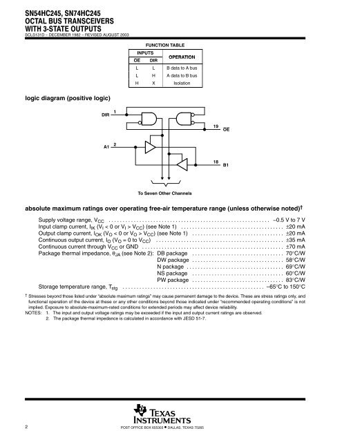
FUNCTION TABLE<br />
INPUTS<br />
OE DIR<br />
OPERATION<br />
L L B data to A bus<br />
L H A data to B bus<br />
H X Isolation<br />
logic diagram (positive logic)<br />
DIR<br />
1<br />
19<br />
OE<br />
A1<br />
2<br />
18<br />
B1<br />
To Seven Other Channels<br />
absolute maximum ratings over operating free-air temperature range (unless otherwise noted) †<br />
Supply voltage range, V CC . . . . . . . . . . . . . . . . . . . . . . . . . . . . . . . . . . . . . . . . . . . . . . . . . . . . . . . . . . −0.5 V to 7 V<br />
Input clamp current, I IK (V I < 0 or V I > V CC ) (see Note 1) . . . . . . . . . . . . . . . . . . . . . . . . . . . . . . . . . . . . . ±20 mA<br />
Output clamp current, I OK (V O < 0 or V O > V CC ) (see Note 1) . . . . . . . . . . . . . . . . . . . . . . . . . . . . . . . . . ±20 mA<br />
Continuous output current, I O (V O = 0 to V CC ) . . . . . . . . . . . . . . . . . . . . . . . . . . . . . . . . . . . . . . . . . . . . . . ±35 mA<br />
Continuous current through V CC or GND . . . . . . . . . . . . . . . . . . . . . . . . . . . . . . . . . . . . . . . . . . . . . . . . . . . ±70 mA<br />
Package thermal impedance, θ JA (see Note 2): DB package . . . . . . . . . . . . . . . . . . . . . . . . . . . . . . . . . 70°C/W<br />
DW package . . . . . . . . . . . . . . . . . . . . . . . . . . . . . . . . . 58°C/W<br />
N package . . . . . . . . . . . . . . . . . . . . . . . . . . . . . . . . . . . 69°C/W<br />
NS package . . . . . . . . . . . . . . . . . . . . . . . . . . . . . . . . . 60°C/W<br />
PW package . . . . . . . . . . . . . . . . . . . . . . . . . . . . . . . . . 83°C/W<br />
Storage temperature range, T stg . . . . . . . . . . . . . . . . . . . . . . . . . . . . . . . . . . . . . . . . . . . . . . . . . . . −65°C to 150°C<br />
† Stresses beyond those listed under “absolute maximum ratings” may cause permanent damage to the device. These are stress ratings only, and<br />
functional operation of the device at these or any other conditions beyond those indicated under “recommended operating conditions” is not<br />
implied. Exposure to absolute-maximum-rated conditions for extended periods may affect device reliability.<br />
NOTES: 1. The input and output voltage ratings may be exceeded if the input and output current ratings are observed.<br />
2. The package thermal impedance is calculated in accordance with JESD 51-7.<br />
2 POST OFFICE BOX 655303 • DALLAS, TEXAS 75265