A new type of tactile sensor detecting contact force and hardness of an
A new type of tactile sensor detecting contact force and hardness of an
A new type of tactile sensor detecting contact force and hardness of an

Create successful ePaper yourself
Turn your PDF publications into a flip-book with our unique Google optimized e-Paper software.
A NEW TYPE OF TACTILE SENSOR DETECTING<br />
CONTACT FORCE AND HARDNESS OF AN OBJECT<br />
T. Shimizu, M. Shikida*, K. Sato, <strong><strong>an</strong>d</strong> K. Itoigawa**<br />
Dept. <strong>of</strong> Micro System Eng., Nagoya University, Chikusa, Nagoya 464-8603, Jap<strong>an</strong>.<br />
* Research Center for Adv<strong>an</strong>ced Waste <strong><strong>an</strong>d</strong> Emission M<strong>an</strong>agement, Nagoya University, Jap<strong>an</strong><br />
**Tokai Rika Co., Ltd., Toyoda, Oguchi, Aichi 480-01 95, Jap<strong>an</strong><br />
ABSTRACT<br />
We propose a <strong>new</strong> <strong>type</strong> <strong>of</strong> <strong>tactile</strong> <strong>sensor</strong> that c<strong>an</strong> detect<br />
both the <strong>contact</strong>-<strong>force</strong> <strong><strong>an</strong>d</strong> <strong>hardness</strong> <strong>of</strong> <strong>an</strong> object. It consists<br />
<strong>of</strong> a diaphragm with a mesa structure, a piezo-resistive<br />
displacement <strong>sensor</strong> on the diaphragm, <strong><strong>an</strong>d</strong> a chamber for<br />
pneumatical actuation. An array <strong>of</strong> these <strong>sensor</strong>s c<strong>an</strong> detect<br />
the two-dimensional <strong>contact</strong>-<strong>force</strong>-distribution <strong><strong>an</strong>d</strong><br />
<strong>hardness</strong>-distribution information, <strong><strong>an</strong>d</strong> the surface texture<br />
<strong>of</strong> the <strong>contact</strong>ed object. We theoretically <strong>an</strong>alyzed the<br />
operation <strong>of</strong> the <strong>tactile</strong> <strong>sensor</strong>, <strong><strong>an</strong>d</strong> designed its specifications<br />
for a device for <strong>detecting</strong> the touch <strong>of</strong> a hum<strong>an</strong> finger. We<br />
fabricated the device’s <strong>sensor</strong> element by micromachining<br />
technologies to prove the principle. The size is 3.0 mm x<br />
3.0 mm x 0.4 mm, <strong><strong>an</strong>d</strong> it has a displacement <strong>sensor</strong> element<br />
<strong>of</strong> piezo-resist<strong>an</strong>ce at the periphery <strong>of</strong> the diaphragm<br />
structure.<br />
INTRODUCTION<br />
MEMS (Micro-Electro-Mech<strong>an</strong>ical-Sy stems) technologes<br />
have opened the door to m<strong>an</strong>y kinds <strong>of</strong> intelligent solidstate<br />
micro<strong>sensor</strong>s, in which the sensing devices are<br />
integrated with electrical circuits on the same wafer. A <strong>tactile</strong><br />
sensing device is a promising area in the field <strong>of</strong> physical<br />
<strong>sensor</strong> systems, because we c<strong>an</strong> make a sensing device that<br />
has functions similar to the surface <strong>of</strong> a fingertip by<br />
integrating micro-scale sensing devices in <strong>an</strong> array.<br />
Several <strong>type</strong>s <strong>of</strong> <strong>tactile</strong> <strong>sensor</strong>s have already been proposed<br />
for h<strong><strong>an</strong>d</strong>ling objects in robotics <strong><strong>an</strong>d</strong> automation systems<br />
[ 1-61. Such devices basically detect the <strong>contact</strong>-<strong>force</strong><br />
between the <strong>sensor</strong> <strong><strong>an</strong>d</strong> objects. Those systems c<strong>an</strong>not,<br />
however, measure the <strong>hardness</strong> <strong>of</strong> the <strong>contact</strong>ed objects.<br />
Therefore, it is difficult for them to h<strong><strong>an</strong>d</strong>le s<strong>of</strong>t <strong><strong>an</strong>d</strong> fragile<br />
materials. Maezawa et al. proposed a <strong>hardness</strong> <strong>detecting</strong><br />
system using a piezoelectric resonator [7], but it has<br />
difficulty <strong>detecting</strong> the <strong>contact</strong> <strong>force</strong> as well as the <strong>hardness</strong><br />
<strong>of</strong> the <strong>contact</strong>ed object.<br />
This paper proposes a <strong>new</strong> <strong>type</strong> <strong>of</strong> <strong>tactile</strong> <strong>sensor</strong> that c<strong>an</strong><br />
detect both the <strong>contact</strong>-<strong>force</strong> <strong><strong>an</strong>d</strong> <strong>hardness</strong> <strong>of</strong> <strong>an</strong> object.<br />
Setting multiple <strong>sensor</strong> devices in <strong>an</strong> array also enables them<br />
to detect the two-dimensional <strong>contact</strong>-<strong>force</strong>-distribution,<br />
<strong>hardness</strong>-distribution, <strong><strong>an</strong>d</strong> surface texture <strong>of</strong> the <strong>contact</strong>ed<br />
object.<br />
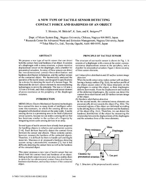
PRINCIPLE OF TACTILE SENSOR<br />
The structure <strong>of</strong> our <strong>tactile</strong> <strong>sensor</strong> is shown in Fig. 1. It<br />
consists <strong>of</strong> a diaphragm with a mesa at the center, a piezoresist<strong>an</strong>ce<br />
displacement <strong>sensor</strong> at the periphery, <strong><strong>an</strong>d</strong> a<br />
chamber for pneumatical actuation. Figure 2 shows <strong>an</strong> array<br />
<strong>of</strong> three <strong>sensor</strong> elements.<br />
(u) Contact-<strong>force</strong> distribution <strong><strong>an</strong>d</strong> 2D ,su&k~ texture imuge<br />
detection<br />
When the <strong>tactile</strong> <strong>sensor</strong> array makes <strong>contact</strong> with <strong>an</strong> object<br />
having a bumpy surface (Fig. 2(a)), the surface pr<strong>of</strong>ile <strong>of</strong><br />
the object causes some <strong>of</strong> the mesa structures on the<br />
diaphragms to <strong>contact</strong> the object, so their diaphragms<br />
deform downwards. From the displacement <strong><strong>an</strong>d</strong> location<br />
<strong>of</strong> the deformed diaphragms, the system c<strong>an</strong> detect the<br />
<strong>contact</strong>-<strong>force</strong> distribution <strong><strong>an</strong>d</strong> 2D surface texture image<br />
<strong>of</strong> the object.<br />
(b) Hurdness distribution detection<br />
In the second mode, the <strong>contact</strong>ed mesa elements are<br />
pneumatically driven towards the object (Fig. 2(b)). The<br />
<strong>contact</strong>ed regions <strong>of</strong> the object are deformed according<br />
to the driving <strong>force</strong> <strong>of</strong> the mesa element <strong><strong>an</strong>d</strong> the <strong>hardness</strong><br />
<strong>of</strong> the object (Fig. 2(c)). Therefore, we c<strong>an</strong> detect the<br />
<strong>hardness</strong> distribution <strong>of</strong> the object by measuring the<br />
relationship between the displacements <strong>of</strong> the diaphragms<br />
<strong><strong>an</strong>d</strong> the actuation <strong>force</strong> <strong>of</strong> the mesa elements.<br />
Piezo-resis t<strong>an</strong>ce J MTDiapbagm<br />
/<br />
pneumatical<br />
Chamber for<br />
actuation<br />
Gas<br />
Gas port<br />
Fig. 1. Structure ($the propaved fuctile .sen.soI:<br />
0-7803-7185-2/02/$10.00 02002 IEEE 344
1 Contact No-<strong>contact</strong> Contact<br />
Arrayed active <strong>tactile</strong> <strong>sensor</strong><br />
(a) Detecting <strong>contact</strong> <strong>force</strong> distribution <strong><strong>an</strong>d</strong> two<br />
dimensional surface image<br />
Fig. 3. Functionul model <strong>of</strong> sensing element.<br />
&as<br />
Cas<br />
Deformation No-deformation Deformation<br />
(b) Detecting <strong>hardness</strong> distribution<br />
t<br />
S<strong>of</strong>t object<br />
according to the pushing depth <strong>of</strong> the mesa structure toward<br />
the object. In this condition, K, is given by<br />
2aE,<br />
K,=- ,<br />
I-y2<br />
where u is the radius <strong>of</strong> the mesa structure <strong><strong>an</strong>d</strong> E, <strong><strong>an</strong>d</strong> v, are<br />
the elastic modulus <strong><strong>an</strong>d</strong> Poisson's ratio <strong>of</strong> the object,<br />
respectively. The elastic const<strong>an</strong>t <strong>of</strong> the diaphragm structure<br />
with mesa is given by<br />
Driving <strong>force</strong> to diaphragm<br />
Hard object<br />
(c) Displacement <strong>of</strong> a diaphragm as a function <strong>of</strong><br />
<strong>hardness</strong> <strong>of</strong> the object<br />
Fig. 2. Detecting principle <strong>of</strong> the proposed <strong>tactile</strong> sensol:<br />
DEVICE DESIGN<br />
We theoretically <strong>an</strong>alyzed the operation <strong>of</strong> the <strong>sensor</strong>, <strong><strong>an</strong>d</strong><br />
designed its specifications to detect the touch <strong>of</strong> a hum<strong>an</strong><br />
finger. First, we modeled the <strong>tactile</strong> <strong>sensor</strong> as shown in Fig.<br />
3. We assumed that the <strong>contact</strong>ed object is <strong>an</strong> elastic<br />
material. The relationship between the deformation X <strong>of</strong><br />
the object <strong><strong>an</strong>d</strong> applied <strong>force</strong> F is given by<br />
F = (K,, + K,
We conclude that in order to detect a ch<strong>an</strong>ge in the <strong>hardness</strong><br />
<strong>of</strong> the touched object, the elastic const<strong>an</strong>t <strong>of</strong> the diaphragm<br />
should be almost the same as that <strong>of</strong> the touched object.<br />
Based on this result, we obtained equation (4), which lets<br />
us determine the diaphragm size. From equations (2) <strong><strong>an</strong>d</strong><br />
(3), <strong><strong>an</strong>d</strong> the choice <strong>of</strong> Kd=K,, the relationship between the<br />
radius <strong><strong>an</strong>d</strong> thickness <strong>of</strong> the diaphragm is given by equation<br />
(4).<br />
The procedure for determining the diaphragm specifications<br />
is as follows.<br />
(1) First, we determined from <strong>an</strong>other experiment that K,s<br />
<strong>of</strong> a fingertip is 330a (kN/m).<br />
(2) Using KS=330a (kN/m), we plotted the relationship<br />
between diaphragm radius <strong><strong>an</strong>d</strong> thickness (equation (4))<br />
to determine the size <strong>of</strong> a <strong>sensor</strong> device that c<strong>an</strong> detect<br />
the <strong>hardness</strong> <strong>of</strong> a fingertip (Fig. 5).<br />
(3) We determined that its minimum thickness is 6.0 pm<br />
because <strong>of</strong> the diffusion depth <strong>of</strong> the piezo-resist<strong>an</strong>ce<br />
layer formed on the diaphragm.<br />
(4) Finally, we chose the diaphragm radius as 1 .O mm, <strong><strong>an</strong>d</strong><br />
designed three different <strong>type</strong>s <strong>of</strong> <strong>sensor</strong>s, which are<br />
shown in Fig. 5.<br />
(a) An n-<strong>type</strong> 4" silicon wafer with resistivity <strong>of</strong>20.4 ficm<br />
was used for fabricating the <strong>sensor</strong>. First, we formed a<br />
silicon oxide layer 500 nm thick on the surface by<br />
thermal oxidization. We patterned it to define the area<br />
<strong>of</strong> the piezo-resist<strong>an</strong>ce sensing elements. Then, we<br />
diffused boron into the opened area <strong>of</strong> the silicon oxide<br />
layer to form p-<strong>type</strong> silicon. The diffused area works as<br />
the displacement <strong>sensor</strong> <strong>of</strong> the diaphragm.<br />
(b) The surface was covered with <strong>an</strong> oxide layer 800 nm<br />
thick, Then a silicon nitride layer was deposited on only<br />
the rear side <strong>of</strong> the wafer. This keeps the rear wafer<br />
surface flat during the following process.<br />
(c) Contact holes were patterned on the front side surface.<br />
Then, for the electrical wiring, <strong>an</strong> AI layer 1 .O pm thick<br />
was deposited by sputtering <strong><strong>an</strong>d</strong> patterned by wet<br />
etching. Finally the surface was covered with a silicon<br />
nitride layer 300 nm thick for protection against the<br />
environment.<br />
(d) The bonding pads for the electrical wiring were patterned<br />
on the front side <strong>of</strong> the wafer, <strong><strong>an</strong>d</strong> the rear side layers<br />
(silicon oxide <strong><strong>an</strong>d</strong> silicon nitride) were patterned to<br />
define the aperture <strong>of</strong> the diaphragm.<br />
Points o! designed devices<br />
Table 1 shows the typical specifications <strong>of</strong> the <strong>sensor</strong><br />
designed for <strong>detecting</strong> the touch <strong>of</strong> a fingertip.<br />
FABRICATION PROCESS<br />
We developed a fabrication process for the <strong>sensor</strong> element<br />
<strong>of</strong>the proposed <strong>tactile</strong> device system to confirm the principle<br />
(Fig. 6). The process is summarized as follows.<br />
"0 0.5 I .o I .5<br />
Radius <strong>of</strong> diaphragm: r (mm)<br />
Fig. 5. Relationship between the rudius und the thickness<br />
<strong>of</strong> diuphrugm suitable for <strong>detecting</strong> hurdnexs ($u hum<strong>an</strong><br />
finger tip (K.s=Kd Ks=330u (kN/m)).<br />
Table I. SpeciJicutions ($<strong>sensor</strong> device.<br />
Elastic const<strong>an</strong>t Ks <strong>of</strong> object<br />
Fig. 4. Relutionship between the defiwmution und elustic<br />
constunt <strong>of</strong>the object. K,y: elustic constunt <strong>of</strong>the object,<br />
Kd. elustic constunt <strong>of</strong>the diuphrugm.<br />
Device<br />
3.0 mm x 3.0 mm x 0.425 mm<br />
Diaphragm 1.0 mm x 1.0 mm x 6.0 pm<br />
Mesa (SU-8) 0.1 mmxO.lmmx30pm<br />
Piezo-resist<strong>an</strong>ce<br />
displacement <strong>sensor</strong><br />
0.10 mm x 0.16 mm<br />
(Resit<strong>an</strong>ce 920 Q)<br />
Elastic const Kd 960 - 1400 N/m<br />
346
Piczo-rcsist<strong>an</strong>cc<br />
SU-8<br />
Fig. 7. Fuhricuted <strong>sensor</strong> device.<br />
‘ Diaphragm<br />
n<br />
Fig. 6. Fabrication process <strong>of</strong> a sensing element.<br />
n-Si<br />
p-Si<br />
SiO,<br />
Si3N4<br />
A1<br />
SU-8<br />
(e) A mesa structure 30 pm high was formed using SU-8<br />
photoresist.<br />
(f) The diaphragm structure IC15 pm thick was formed<br />
by wet etching using 30.5 wt.% KOH as the etching<br />
solution <strong><strong>an</strong>d</strong> <strong>an</strong> etching temperature <strong>of</strong> 90°C. The front<br />
side <strong>of</strong>the wafer was protected from attack by the etching<br />
solution.<br />
The fabricated sensing device is shown in Fig. 7. It is 3.0<br />
mm x 3.0 mm <strong><strong>an</strong>d</strong> has a displacement <strong>sensor</strong> <strong>of</strong> piezoresist<strong>an</strong>ce<br />
at the edges <strong>of</strong> the diaphragm structure.<br />
CONCLUSION<br />
We proposed a <strong>new</strong> <strong>type</strong> <strong>of</strong> <strong>tactile</strong> <strong>sensor</strong> that c<strong>an</strong> detect<br />
both the <strong>contact</strong>-<strong>force</strong> <strong><strong>an</strong>d</strong> <strong>hardness</strong> <strong>of</strong> <strong>an</strong> object. We<br />
theoretically <strong>an</strong>alyzed the operation <strong>of</strong> the <strong>tactile</strong> <strong>sensor</strong>,<br />
<strong><strong>an</strong>d</strong> designed its specifications for a device for <strong>detecting</strong><br />
the touch <strong>of</strong> a hum<strong>an</strong> finger. We fabricated the device’s<br />
<strong>sensor</strong> element by micromachining technologies to prove<br />
the principle. The size is 3.0 mm x 3.0 mm x 0.4 mm, <strong><strong>an</strong>d</strong><br />
it has a displacement <strong>sensor</strong> element <strong>of</strong> piezo-resist<strong>an</strong>ce at<br />
the periphery <strong>of</strong> the diaphragm structure.<br />
ACKNOWLEDGEMENTS<br />
This work was carried out under the program <strong>of</strong> research<br />
<strong><strong>an</strong>d</strong> development <strong>of</strong> micro-mechatronics supported by<br />
Chubu Science <strong><strong>an</strong>d</strong> Technology Center, N<strong>an</strong>ova <strong><strong>an</strong>d</strong> was<br />
also partially supported by GrGi-in-Aid for Ekkragement<br />
<strong>of</strong> Young Scientists No. 13750216 from the Ministry <strong>of</strong><br />
Education, Culture, Sports, Science <strong><strong>an</strong>d</strong> Technology.<br />
REFERENCES<br />
[ 11 K. J. Chun <strong><strong>an</strong>d</strong> K. D. Wise, “A capacitive silicon <strong>tactile</strong><br />
image array”, Proc. <strong>of</strong> the 3rd Int. Conf on Solid-state<br />
Sensors <strong><strong>an</strong>d</strong> Actuators, pp. 22-25, 1985.<br />
[2] K. Petersen, C. Kowalski, J. Brown, H. Allen, <strong><strong>an</strong>d</strong> J.<br />
Knutti, “A <strong>force</strong> sensing chip designed for robotic <strong><strong>an</strong>d</strong><br />
m<strong>an</strong>ufacturing automation application”, Proc. <strong>of</strong> the 3rd<br />
Int. Conf. on Solid-state Sensors <strong><strong>an</strong>d</strong> Actuators, pp. 30-<br />
32, 1985.<br />
[3] B. J. K<strong>an</strong>e <strong><strong>an</strong>d</strong> G. T. A. Kovacs, “A CMOS compatible<br />
traction stress sensing element for use in high resolution<br />
<strong>tactile</strong> image”, Proc. <strong>of</strong> the 8th Int. Conf. on Solid-state<br />
Sensors <strong><strong>an</strong>d</strong> Actuators, pp. 648-65 1, 1995.<br />
[4] Z. Chu, P. M. Sarro, <strong><strong>an</strong>d</strong> S. Middlehoek, “Silicon threeaxial<br />
<strong>tactile</strong> <strong>sensor</strong>”, Proc. <strong>of</strong> the 8th Int. Conf. on Solid-<br />
State Sensors <strong><strong>an</strong>d</strong> Actuators, pp. 656-659, 1995.<br />
[5] R. J. De Souza <strong><strong>an</strong>d</strong> K. D. Wise, “A very high density<br />
bulk micromachined capacitive <strong>tactile</strong> imager”, Proc.<br />
<strong>of</strong> the 9th Int. Conf. on Solid-state Sensors <strong><strong>an</strong>d</strong><br />
Actuators, pp. 656-659, 1997.<br />
[6] H. Takizawa, H. Tosaka, R. Ohta, S. K<strong>an</strong>eko, <strong><strong>an</strong>d</strong> Y.<br />
Ueda, “Development <strong>of</strong> a micr<strong>of</strong>ine active bending<br />
catheter equipment with MIF <strong>tactile</strong> <strong>sensor</strong>s”, Proc.<br />
IEEE MEMS’99 conference, pp. 412-41 7, 1999.<br />
[7] M. Maezawa, T. lmahashi, Y. Kuroda, H. Adachi, <strong><strong>an</strong>d</strong><br />
K. Y<strong>an</strong>agisawa, “Tactile <strong>sensor</strong> using piezoelectric<br />
resonator”, Proc. <strong>of</strong> the 9th Int. Conf. on Solid-state<br />
Sensors <strong><strong>an</strong>d</strong> Actuators, pp. 1 1 7- 120, 1997.<br />
347