LM675 Power Operational Amplifier - LENS
LM675 Power Operational Amplifier - LENS
LM675 Power Operational Amplifier - LENS

Create successful ePaper yourself
Turn your PDF publications into a flip-book with our unique Google optimized e-Paper software.
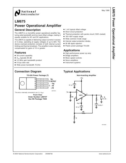
<strong>LM675</strong><strong>Power</strong> <strong>Operational</strong> <strong>Amplifier</strong>General DescriptionThe <strong>LM675</strong> is a monolithic power operational amplifier featuringwide bandwidth and low input offset voltage, making itequally suitable for AC and DC applications.The <strong>LM675</strong> is capable of delivering output currents in excessof 3 amps, operating at supply voltages of up to 60V. Thedevice overload protection consists of both internal currentlimiting and thermal shutdown. The amplifier is also internallycompensated for gains of 10 or greater.Featuresn 3A current capabilityn A VO typically 90 dBn 5.5 MHz gain bandwidth productn 8 V/µs slew raten Wide power bandwidth 70 kHzn 1 mV typical offset voltagen Short circuit protectionn Thermal protection with parole circuit (100% tested)n 16V–60V supply rangen Wide common mode rangen Internal output protection diodesn 90 dB ripple rejectionn Plastic power package TO-220Applicationsn High performance power op ampn Bridge amplifiersn Motor speed controlsn Servo amplifiersn Instrument systemsMay 1999<strong>LM675</strong> <strong>Power</strong> <strong>Operational</strong> <strong>Amplifier</strong>Connection DiagramTO-220 <strong>Power</strong> Package (T)Typical ApplicationsNon-Inverting <strong>Amplifier</strong>*The tab is internally connected to pin 3 (−V EE )Front ViewOrder Number <strong>LM675</strong>TSee NS Package T05D0067390100673902© 2004 National Semiconductor Corporation DS006739 www.national.com
<strong>LM675</strong>Absolute Maximum Ratings (Note 1)If Military/Aerospace specified devices are required,please contact the National Semiconductor Sales Office/Distributors for availability and specifications.Supply Voltage ±30VStorage TemperatureJunction Temperature<strong>Power</strong> Dissipation (Note 2)Lead Temperature(Soldering, 10 seconds)−65˚C to +150˚C150˚C30W260˚CInput Voltage−V EE to V CCESD rating to be determined.Operating Temperature0˚C to +70˚CElectrical CharacteristicsV S =±25V, T A =25˚C unless otherwise specified.Parameter Conditions Typical Tested Limit UnitsSupply Current P OUT = 0W 18 50 (max) mAInput Offset Voltage V CM = 0V 1 10 (max) mVInput Bias Current V CM = 0V 0.2 2 (max) µAInput Offset Current V CM = 0V 50 500 (max) nAOpen Loop Gain R L = ∞Ω 90 70 (min) dBPSRR ∆V S = ±5V 90 70 (min) dBCMRR V IN = ±20V 90 70 (min) dBOutput Voltage Swing R L =8Ω ±21 ±18 (min) VOffset Voltage Drift Versus Temperature R S< 100 kΩ 25 µV/˚COffset Voltage Drift Versus Output <strong>Power</strong> 25 µV/WOutput <strong>Power</strong> THD = 1%, f O = 1 kHz, R L =8Ω 25 20 WGain Bandwidth Product f O = 20 kHz, A VCL = 1000 5.5 MHzMax Slew Rate 8 V/µsInput Common Mode Range ±22 ±20 (min) VNote 1: Absolute Maximum Ratings indicate limits beyond which damage to the device may occur. Operating Ratings indicate conditions for which the device isfunctional, but do not guarantee specific performance limits. Electrical Characteristics state DC and AC electrical specifications under particular test conditions whichguarantee specific performance limits. This assumes that the device is within the Operating Ratings. Specifications are not guaranteed for parameters where no limitis given, however, the typical value is a good indication of device performance.Note 2: Assumes T A equal to 70˚C. For operation at higher tab temperatures, the <strong>LM675</strong> must be derated based on a maximum junction temperature of 150˚C.Typical ApplicationsGenerating a Split Supply From a Single SupplyV S = ±8V → ±30V00673903www.national.com 2
Typical Performance CharacteristicsTHD vs <strong>Power</strong> OutputInput Common ModeRange vs Supply Voltage<strong>LM675</strong>0067391000673911Supply Current vsSupply VoltagePSRR vs Frequency0067391200673913Device Dissipation vsAmbient Temperature†Current Limit vsOutput Voltage*†θ INTERFACE = 1˚ C/WSee Application Hints.00673914*V S = ±25V006739153www.national.com
<strong>LM675</strong>Typical Performance Characteristics (Continued)I B vs Supply VoltageOutput VoltageSwing vs Supply Voltage0067391600673917www.national.com 4
<strong>LM675</strong>Schematic Diagram006739055www.national.com
<strong>LM675</strong>Application HintsSTABILITYThe <strong>LM675</strong> is designed to be stable when operated at aclosed-loop gain of 10 or greater, but, as with any otherhigh-current amplifier, the <strong>LM675</strong> can be made to oscillateunder certain conditions. These usually involve printed circuitboard layout or output/input coupling.When designing a printed circuit board layout, it is importantto return the load ground, the output compensation ground,and the low level (feedback and input) grounds to the circuitboard ground point through separate paths. Otherwise, largecurrents flowing along a ground conductor will generatevoltages on the conductor which can effectively act as signalsat the input, resulting in high frequency oscillation orexcessive distortion. It is advisable to keep the output compensationcomponents and the 0.1 µF supply decouplingcapacitors as close as possible to the <strong>LM675</strong> to reduce theeffects of PCB trace resistance and inductance. For thesame reason, the ground return paths for these componentsshould be as short as possible.Occasionally, current in the output leads (which function asantennas) can be coupled through the air to the amplifierinput, resulting in high-frequency oscillation. This normallyhappens when the source impedance is high or the inputleads are long. The problem can be eliminated by placing asmall capacitor (on the order of 50 pF to 500 pF) across thecircuit input.Most power amplifiers do not drive highly capacitive loadswell, and the <strong>LM675</strong> is no exception. If the output of the<strong>LM675</strong> is connected directly to a capacitor with no seriesresistance, the square wave response will exhibit ringing ifthe capacitance is greater than about 0.1 µF. The amplifiercan typically drive load capacitances up to 2 µF or so withoutoscillating, but this is not recommended. If highly capacitiveloads are expected, a resistor (at least 1Ω) should be placedin series with the output of the <strong>LM675</strong>. A method commonlyemployed to protect amplifiers from low impedances at highfrequencies is to couple to the load through a 10Ω resistor inparallel with a5µHinductor.CURRENT LIMIT AND SAFE OPERATING AREA(SOA) PROTECTIONA power amplifier’s output transistors can be damaged byexcessive applied voltage, current flow, or power dissipation.The voltage applied to the amplifier is limited by the design ofthe external power supply, while the maximum currentpassed by the output devices is usually limited by internalcircuitry to some fixed value. Short-term power dissipation isusually not limited in monolithic operational power amplifiers,and this can be a problem when driving reactive loads, whichmay draw large currents while high voltages appear on theoutput transistors. The <strong>LM675</strong> not only limits current toaround 4A, but also reduces the value of the limit currentwhen an output transistor has a high voltage across it.When driving nonlinear reactive loads such as motors orloudspeakers with built-in protection relays, there is a possibilitythat an amplifier output will be connected to a loadwhose terminal voltage may attempt to swing beyond thepower supply voltages applied to the amplifier. This cancause degradation of the output transistors or catastrophicfailure of the whole circuit. The standard protection for thistype of failure mechanism is a pair of diodes connectedbetween the output of the amplifier and the supply rails.These are part of the internal circuitry of the <strong>LM675</strong>, andneedn’t be added externally when standard reactive loadsare driven.THERMAL PROTECTIONThe <strong>LM675</strong> has a sophisticated thermal protection schemeto prevent long-term thermal stress to the device. When thetemperature on the die reaches 170˚C, the <strong>LM675</strong> shutsdown. It starts operating again when the die temperaturedrops to about 145˚C, but if the temperature again begins torise, shutdown will occur at only 150˚C. Therefore, the deviceis allowed to heat up to a relatively high temperature ifthe fault condition is temporary, but a sustained fault will limitthe maximum die temperature to a lower value. This greatlyreduces the stresses imposed on the IC by thermal cycling,which in turn improves its reliability under sustained faultconditions. This circuitry is 100% tested without a heat sink.Since the die temperature is directly dependent upon theheat sink, the heat sink should be chosen for thermal resistancelow enough that thermal shutdown will not be reachedduring normal operaton. Using the best heat sink possiblewithin the cost and space constraints of the system willimprove the long-term reliability of any power semiconductor.POWER DISSIPATION AND HEAT SINKINGThe <strong>LM675</strong> should always be operated with a heat sink,even though at idle worst case power dissipation will be only1.8W (30 mA x 60V) which corresponds to a rise in dietemperature of 97˚C above ambient assuming θ jA = 54˚C/Wfor a TO-220 package. This in itself will not cause the thermalprotection circuitry to shut down the amplifier when operatingat room temperature, but a mere 0.9W of additional powerdissipation will shut the amplifier down since T J will thenincrease from 122˚C (97˚C + 25˚C) to 170˚C.In order to determine the appropriate heat sink for a givenapplication, the power dissipation of the <strong>LM675</strong> in that applicationmust be known. When the load is resistive, the maximumaverage power that the IC will be required to dissipateis approximately:where V S is the total power supply voltage across the<strong>LM675</strong>, R L is the load resistance and P Q is the quiescentpower dissipation of the amplifier. The above equation isonly an approximation which assumes an “ideal” class Boutput stage and constant power dissipation in all other partsof the circuit. As an example, if the <strong>LM675</strong> is operated on a50V power supply with a resistive load of 8Ω, it can developup to 19W of internal power dissipation. If the die temperatureis to remain below 150˚C for ambient temperatures up to70˚C, the total junction-to-ambient thermal resistance mustbe less thanUsing θ JC = 2˚C/W, the sum of the case-to-heat sink interfacethermal resistance and the heat-sink-to-ambient thermalresistance must be less than 2.2˚C/W. The case-to-heatsinkthermal resistance of the TO-220 package varies withthe mounting method used. A metal-to-metal interface will beabout 1˚C/W if lubricated, and about 1.2˚C/W if dry. If a micainsulator is used, the thermal resistance will be aboutwww.national.com 6
Application Hints (Continued)1.6˚C/W lubricated and 3.4˚C/W dry. For this example, weassume a lubricated mica insulator between the <strong>LM675</strong> andthe heat sink. The heat sink thermal resistance must then beless than4.2˚C/W − 2˚C/W − 1.6˚C/W = 0.6˚C/W.This is a rather large heat sink and may not be practical insome applications. If a smaller heat sink is required forreasons of size or cost, there are two alternatives. Themaximum ambient operating temperature can be restrictedto 50˚C (122˚F), resulting in a 1.6˚C/W heat sink, or the heatsink can be isolated from the chassis so the mica washer isnot needed. This will change the required heat sink to a1.2˚C/W unit if the case-to-heat-sink interface is lubricated.Typical ApplicationsThe thermal requirements can become more difficult whenan amplifier is driving a reactive load. For a given magnitudeof load impedance, a higher degree of reactance will causea higher level of power dissipation within the amplifier. As ageneral rule, the power dissipation of an amplifier driving a60˚ reactive load will be roughly that of the same amplifierdriving the resistive part of that load. For example, somereactive loads may at some frequency have an impedancewith a magnitude of 8Ω and a phase angle of 60˚. The realpart of this load will then be 8Ω x cos 60˚ or 4Ω, and theamplifier power dissipation will roughly follow the curve ofpower dissipation with a 4Ω load.<strong>LM675</strong>Non-Inverting Unity Gain Operation00673906Inverting Unity Gain Operation006739077www.national.com
<strong>LM675</strong>Typical Applications (Continued)Servo Motor Control00673908High Current Source/SinkI OUT =V IN x 2.5 amps/volti.e. I OUT = 1A when V IN = 400 mV00673909Trim pot for max R OUTwww.national.com 8
Physical Dimensions inches (millimeters) unless otherwise noted<strong>LM675</strong> <strong>Power</strong> <strong>Operational</strong> <strong>Amplifier</strong>TO-220 <strong>Power</strong> Package (T)Order Number <strong>LM675</strong>TNS Package T05DNational does not assume any responsibility for use of any circuitry described, no circuit patent licenses are implied and National reservesthe right at any time without notice to change said circuitry and specifications.For the most current product information visit us at www.national.com.LIFE SUPPORT POLICYNATIONAL’S PRODUCTS ARE NOT AUTHORIZED FOR USE AS CRITICAL COMPONENTS IN LIFE SUPPORT DEVICES OR SYSTEMSWITHOUT THE EXPRESS WRITTEN APPROVAL OF THE PRESIDENT AND GENERAL COUNSEL OF NATIONAL SEMICONDUCTORCORPORATION. As used herein:1. Life support devices or systems are devices or systemswhich, (a) are intended for surgical implant into the body, or(b) support or sustain life, and whose failure to perform whenproperly used in accordance with instructions for useprovided in the labeling, can be reasonably expected to resultin a significant injury to the user.2. A critical component is any component of a life supportdevice or system whose failure to perform can be reasonablyexpected to cause the failure of the life support device orsystem, or to affect its safety or effectiveness.BANNED SUBSTANCE COMPLIANCENational Semiconductor certifies that the products and packing materials meet the provisions of the Customer Products StewardshipSpecification (CSP-9-111C2) and the Banned Substances and Materials of Interest Specification (CSP-9-111S2) and contain no ‘‘BannedSubstances’’ as defined in CSP-9-111S2.National SemiconductorAmericas CustomerSupport CenterEmail: new.feedback@nsc.comTel: 1-800-272-9959www.national.comNational SemiconductorEurope Customer Support CenterFax: +49 (0) 180-530 85 86Email: europe.support@nsc.comDeutsch Tel: +49 (0) 69 9508 6208English Tel: +44 (0) 870 24 0 2171Français Tel: +33 (0) 1 41 91 8790National SemiconductorAsia Pacific CustomerSupport CenterEmail: ap.support@nsc.comNational SemiconductorJapan Customer Support CenterFax: 81-3-5639-7507Email: jpn.feedback@nsc.comTel: 81-3-5639-7560