'Thin films & coatings' Roadmap - Nano Mahidol
'Thin films & coatings' Roadmap - Nano Mahidol
'Thin films & coatings' Roadmap - Nano Mahidol

You also want an ePaper? Increase the reach of your titles
YUMPU automatically turns print PDFs into web optimized ePapers that Google loves.
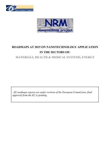
ROADMAPS AT 2015 ON NANOTECHNOLOGY APPLICATION<br />
IN THE SECTORS OF:<br />
MATERIALS, HEALTH & MEDICAL SYSTEMS, ENERGY<br />
All roadmaps reports are under revision of the European Commission, final<br />
approval from the EC is pending.
<strong>Nano</strong>RoadMap is a project co-funded by the 6th Framework Programme of the EC<br />
<strong>Roadmap</strong> Report on Thin <strong>films</strong> & coatings<br />
AIRI/<strong>Nano</strong>tec IT<br />
Willems & van den Wildenberg (ES/NL)<br />
VDI/VDE (DE)<br />
Institute of <strong>Nano</strong>technology (UK)<br />
MATIMOP (IL)<br />
Technology Centre (CZ)<br />
VTT (FI)<br />
Yole Dèveloppement (FR)<br />
Author: Willems & van den Wildenberg (W&W)<br />
November 2005
W&W España s.l.<br />
Avda. Diagonal 361<br />
E-08037 Barcelona, Spain<br />
[t] +34 93 208 21 36<br />
[f] +34 93 208 21 37<br />
[e] contact@wywes.com<br />
[u] www.wywes.com<br />
Authored by:<br />
Carles Escolano<br />
&<br />
Juan Pérez<br />
&<br />
Laszlo Bax<br />
The present document is a roadmap report prepared by Willems & van den<br />
Wildenberg (W&W) in the framework of the <strong>Nano</strong>RoadMap (NRM) project, cofunded<br />
by the 6th Framework Programme (FP6) of the European Commission.<br />
This roadmap report is mainly based on the input received from experts<br />
participating in a Delphi-like panel. In addition, W&W has added where relevant<br />
its views and opinions, in each case identifying clearly the status of such<br />
statement. The views expressed do not necessarily reflect those of the European<br />
Commission.<br />
2 <strong>Roadmap</strong> report on<br />
Thin <strong>films</strong> and coatings
Table of contents<br />
1 Introduction ................................................................................................................................4<br />
1.1 Background......................................................................................................................4<br />
1.2 Goals ................................................................................................................................4<br />
1.3 Methodology ....................................................................................................................4<br />
1.3.1 Collection and synthesis of relevant existing information...................................4<br />
1.3.2 Selection of topics .................................................................................................5<br />
1.3.3 <strong>Roadmap</strong>s elaboration..........................................................................................5<br />
1.4 Structure of this report ....................................................................................................6<br />
2 ‘Thin <strong>films</strong> & coatings’ <strong>Roadmap</strong>..............................................................................................7<br />
2.1 Definition of thin <strong>films</strong> ......................................................................................................7<br />
2.2 Most remarkable properties of thin <strong>films</strong>........................................................................8<br />
2.3 The Thin <strong>films</strong> & coatings’ pipeline ............................................................................. 10<br />
2.3.1 Thin <strong>films</strong>’ production & application .................................................................. 12<br />
2.3.2 Thin <strong>films</strong>’ post-treatment .................................................................................. 17<br />
2.3.3 Patterning methods ............................................................................................ 19<br />
2.3.4 Thin <strong>films</strong>’ applications....................................................................................... 23<br />
2.4 Non technological aspects........................................................................................... 36<br />
2.4.1 Legal aspects (incl. patenting systems)............................................................ 36<br />
2.4.2 Infrastructure requirements and instrumentation cost ..................................... 36<br />
2.4.3 Health, safety and environmental aspects ....................................................... 38<br />
2.5 Conclusions .................................................................................................................. 39<br />
2.5.1 Most relevant applications ................................................................................. 39<br />
2.5.2 EU positioning in the field .................................................................................. 40<br />
2.5.3 Final conclusions and recommendations ......................................................... 41<br />
Annex I. List of Participants.......................................................................................................... 46<br />
Annex II. Participants’ background .............................................................................................. 48<br />
3 <strong>Roadmap</strong> report on<br />
Thin <strong>films</strong> and coatings
1 Introduction<br />
1.1 Background<br />
The <strong>Nano</strong>RoadMap (NRM) project, co-funded by the European Commission (EC), is<br />
aimed at roadmapping nanotechnology related applications in three different areas:<br />
- Materials<br />
- Health & Medical Systems<br />
- Energy<br />
Within the project, an international consortium consisting of eight partners covering<br />
seven European countries and Israel has joined forces to cover the timeframe for<br />
technological development in this field up to 2015. The results of the NRM project are<br />
to be used by any European entity interested in planning an R&D strategy taking into<br />
account nanotechnology. An important potential user is of course the EC itself in the<br />
preparation of the 7th Framework Programme (FP7) for research and technology<br />
development.<br />
For additional information on the NRM project, please refer to www.nanoroadmap.it<br />
1.2 Goals<br />
The primary objective of NRM is to provide coherent scenarios and technology<br />
roadmaps that could help the European players to optimise the positive impact of<br />
nanotechnology on society, giving the necessary knowledge on its future<br />
development and when technologies and applications will come into full fruition.<br />
The key users of the reports are mainly European industry including SMEs, research<br />
organisations, and public bodies in general and the EC in particular.<br />
This report is one of the three final deliverables of the NRM project (together with the<br />
reports on the fields of Health & Medical Systems and Energy) and it is aimed at<br />
providing a thorough overview of specific topics selected for roadmapping within the<br />
field.<br />
1.3 Methodology<br />
1.3.1 Collection and synthesis of relevant existing information<br />
A report was published in October 2004, as the most important deliverable of the first<br />
stage of the project. It was based on the collection and synthesis of existing public<br />
sources in 31 countries and was published as key input for the celebration of the<br />
First NRM International Conference held in Rome the 4 th – 5 th of November 2004.<br />
The full report can be downloaded for free on the project web site.<br />
The report focused on reviewing the different types of nanomaterials, describing the<br />
topic, its most remarkable properties, current and future markets & applications, and<br />
leading countries & highlighted R&D activities in the field. A general review of non-<br />
4 <strong>Roadmap</strong> report on<br />
Thin <strong>films</strong> and coatings
technological aspects (social, legal, ethical and health and safety aspects, but also<br />
economical aspects and infrastructures requirements) was also performed.<br />
The 12 topics identified, even if not being completely homogenous in terms of scope<br />
or materials classification, were intended to adequately cover the field of<br />
nanomaterials. The following list was agreed upon the different partners of the NRM<br />
project (similar classifications can be found in the existing bibliography):<br />
• <strong>Nano</strong>structured materials<br />
• <strong>Nano</strong>particles / nanocomposites<br />
• <strong>Nano</strong>capsules<br />
• <strong>Nano</strong>porous materials<br />
• <strong>Nano</strong>fibres<br />
• Fullerenes<br />
• <strong>Nano</strong>wires<br />
• Single-Walled & Multi-Walled (Carbon) <strong>Nano</strong>tubes<br />
• Dendrimers<br />
• Molecular Electronics<br />
• Quantum Dots<br />
• Thin Films<br />
1.3.2 Selection of topics<br />
Another major goal of that report was to set the basis for discussion and selection for<br />
roadmapping of 4 out of the 12 topics identified above. A preliminary selection of<br />
topics was presented during the First International Conference in November 2004.<br />
After a thorough discussion, which involved international experts in the field of<br />
nanotechnology, four topics were selected (and validated in dialogue with the<br />
European Commission). The topics chosen are:<br />
• <strong>Nano</strong>porous materials<br />
• <strong>Nano</strong>particles / nanocomposites<br />
• Dendrimers<br />
• Thin Films & coatings<br />
1.3.3 <strong>Roadmap</strong>s elaboration<br />
A Delphi-like approach (hereafter referred to as Delphi panel) has been used for the<br />
preparation and execution of the roadmaps. The methodology followed consisted of<br />
2 cycles, and it was the same for the four topics. The Delphi exercise consisted in:<br />
1. Selecting top-international experts in the field (see the annexes for more<br />
information)<br />
2. Preparing a dedicated on-line questionnaire for each topic to be roadmapped<br />
3. Circulating the questionnaire and gathering experts’ responses (1 st cycle)<br />
5 <strong>Roadmap</strong> report on<br />
Thin <strong>films</strong> and coatings
4. Preparing a first draft roadmap document based on the input gathered from<br />
the experts and personal interviews with some experts<br />
5. Circulating the draft roadmap document, asking for feedback (2 nd cycle)<br />
6. Elaborating the final version of the roadmap<br />
One roadmap has been prepared for each of the four aforementioned topics. These<br />
roadmaps are/ have been presented in 8 National Conferences and one International<br />
Conference during the 4 th quarter of 2005.<br />
1.4 Structure of this report<br />
This roadmap begins with the definition of thin <strong>films</strong> and coatings (section 2.1) and<br />
the identification and description of their most remarkable properties (2.2). Wherever<br />
possible, concrete applications have been linked to potential offered by new or<br />
improved thin <strong>films</strong>’ properties.<br />
Section 2.3 focuses on the thin <strong>films</strong>’ pipeline, including production & application<br />
(2.3.1), post-treatment (2.3.2) patterning application (2.3.3) and market applications<br />
(2.3.4) steps. For each of these steps, we have detailed most relevant technologies<br />
and main barriers pointed out by the experts. Whenever possible, we have also<br />
identified ways to overcome these (breakthroughs). In the applications section, we<br />
have provided a list of the most common applications being researched worldwide.<br />
Detailed graphics (based on the input from the experts) provide an overview of the<br />
(estimated) state of development of these applications in 2005, 2010 and 2015.<br />
Additionally, we have included a graph representing the risk involved against the<br />
expected market growth of each application during the next decade.<br />
Section 2.4 briefly reviews non-technological aspects of thin <strong>films</strong> and coatings. We<br />
have not focused in this chapter too much, since other initiatives / projects already<br />
cover them.<br />
The last section (2.5) is devoted to conclusions and recommendations. It includes the<br />
review of the most relevant applications (2.5.1), the EU positioning in the field (2.5.2)<br />
and final conclusions and recommendations (2.5.3). Annexes at the end of the<br />
document include the list of participants in the Delphi and their background.<br />
In this document, certain pieces of text have been highlighted to capture the reader’s<br />
attention. Text highlighted reflects that, according to W&W’s opinion, there is a topic<br />
there suitable for future FP7 research.<br />
6 <strong>Roadmap</strong> report on<br />
Thin <strong>films</strong> and coatings
2 ‘Thin <strong>films</strong> & coatings’ <strong>Roadmap</strong><br />
2.1 Definition of thin <strong>films</strong><br />
This chapter focuses on material structures<br />
resulting from the deposition of one or more<br />
material layers onto a surface. The thickness of<br />
the thin <strong>films</strong> considered is below the order of<br />
100 nm.<br />
Typical production processes are physical<br />
vapour deposition (PVD), chemical vapour<br />
deposition (CVD) or sol-gel. Lately, many<br />
research groups are looking at the possibilities<br />
for printing technologies to create functional<br />
(patterned) thin <strong>films</strong>.<br />
Flexible display using ultra-thin back<br />
plane with thin film transistors,<br />
Courtesy of Philips<br />
Materials used include Si <strong>films</strong> (amorphous, crystalline or polycrystalline), Fe3O4<br />
(magnetite) and other metal/metal-oxides (for magnetism-related applications),<br />
YBCO (superconductivity), diamond (scratch resistance), selenides or metal sulfides<br />
(applications exploiting luminescence properties). Finally, there’s a wide range of<br />
(nano) particles formerly used in (nano)coatings that are being reconsidered; for<br />
instance, Tungsten Oxide may be replaced by ZnO thin <strong>films</strong>.<br />
Not surprisingly, polymer thin <strong>films</strong> are very much investigated. There are some<br />
important reasons behind this fact. They are applicable in a huge variety of<br />
applications, ranging from the electronic sector as photo-resist in semiconductor<br />
wafer’s production process and as inter-metallic (low-k) dielectrics in Integrated<br />
Circuits, right through organic light emitting displays (OLEDs) up to simple anticorrosion<br />
coatings. Moreover, organic thin <strong>films</strong> can be applied at low temperature<br />
(as compared to ceramic/inorganic materials) and therefore can be handled by less<br />
sophisticated processes (e.g. sol-gel).<br />
By adding inorganic fillers to organic thin <strong>films</strong>, mechanical properties can be<br />
improved. Normally this would mean sacrificing flexibility and transparency properties<br />
7 <strong>Roadmap</strong> report on<br />
Thin <strong>films</strong> and coatings
of organic materials; however, nanotechnology allows retention of these properties,<br />
with regard to transparency mainly because the particles are smaller than the<br />
wavelengths of visible light.<br />
2.2 Most remarkable properties of thin <strong>films</strong><br />
The main advantage of thin <strong>films</strong> (or any other coating) is that materials properties<br />
can be transferred to the surface (thus enabling the use of diverse substrates). The<br />
substrate and the thin film are a material system where each of them provides the<br />
required functionality.<br />
In general, nanotechnology provides the tools for controlling 3 key parameters for<br />
thin <strong>films</strong> performance: chemical composition (and crystalline structure at nano-sized<br />
domains), thickness and topography (including nano-scale patterning of thin <strong>films</strong>’<br />
surface).<br />
According to the experts, most remarkable thin film properties are: optical,<br />
mechanical and chemical properties. Monolayer thin <strong>films</strong> could, most of the times,<br />
provide these properties, although multi-layer thin <strong>films</strong> are sometimes required. Of<br />
course, in many applications, it is exactly the combination of properties (often the<br />
transparency combined with chemical or mechanical properties) that exploits the<br />
nanoscale most.<br />
Chemical properties<br />
Thin <strong>films</strong> could be designed to have properties like water repellence, anti-fogging,<br />
chemical barriers and chemical inertness, oxygen or moisture barriers over polymers<br />
or antimicrobial surfaces. The functionalisation of polar/apolar surfaces is crucial for<br />
sensors’ applications and together with hydrophilic/hydrophobic balances is essential<br />
in hard coatings. By increasing the inorganic content, thin film stability could also be<br />
improved. The appropriate chemical composition (e.g. hybrid coatings) also provides<br />
good etch barrier characteristics (e.g. for plastics on automotive bodies) or has also a<br />
great impact on electrical properties (e.g. in SiOxNy) and especially on insulation<br />
properties (relevant for semiconductor circuit structures).<br />
8 <strong>Roadmap</strong> report on<br />
Thin <strong>films</strong> and coatings
Optical properties<br />
These include a.o. light emission, trapping, transmission, opaqueness, fluorescence,<br />
waveguides, anti reflection, etc. Some thin <strong>films</strong> have the ability to emit light without<br />
the need for a backlight; these are applied in displays. Thin <strong>films</strong> can be designed to<br />
be transparent or opaque (or both depending on the applied voltage or incident light)<br />
and applied, a.o. in windows, displays or solar cells. In some cases multi-layered thin<br />
<strong>films</strong> are required for achieving the desired properties (e.g. OLEDs use small<br />
molecules in multi-layers for up to full colour displays). Thin <strong>films</strong> of high refractive<br />
materials could be designed to be planar waveguides for photonics’ applications.<br />
Dielectric thin <strong>films</strong> could also be used to generate surface plasmons resonance<br />
that’s exploitable in optical modulators or chemical sensors. <strong>Nano</strong>technology enables<br />
a precise knowledge on the exact thickness required for desired optical and/or<br />
electrical properties. The interface between the thin film/layer and the substrate is<br />
crucial for understanding the optical (but also) electrical behaviour at ever decreasing<br />
thicknesses and for optimising the layer thickness.<br />
Mechanical properties<br />
These include a.o. wear/ abrasion resistance, hardness, scratch resistance, dry<br />
lubrication, reduced Strain-to-failure, etc. Surface heterogeneities of either chemical<br />
or morphological origin drastically affect interface phenomena (wetting-adhesionfriction).<br />
<strong>Nano</strong>technology enables the design and production of thin <strong>films</strong> with the<br />
required thickness and topography.<br />
Electrical (conductivity, insulation, etc.) and magnetic properties:<br />
Highly dependent on the chemical composition, some thin <strong>films</strong>’ high conductivity<br />
properties are of great importance for CMOS’ wiring materials or for OLEDs. The<br />
dielectric characteristic of some thin <strong>films</strong>’ material is exploited together with<br />
magnetic properties in high-density storage and non-volatile memory applications.<br />
<strong>Nano</strong>technology in this area enables the preparation of thinner <strong>films</strong> as well as a<br />
better dispersion of magnetic particles.<br />
Thermal properties<br />
Thin film coatings are applied in windows or more sophisticated applications like<br />
aircraft engines (e.g. Thermal Barrier Coatings based on Zirconia). <strong>Nano</strong>technology<br />
enables the optimisation of thin film thickness and density (incl. pores, if any) to<br />
specific requirements. Application of multi-layered thin <strong>films</strong> allows, for instance,<br />
blocking the travel of atomic vibrations that produces heat flow whilst still letting the<br />
electrons flow as a current (application in thermoelectric devices).<br />
9 <strong>Roadmap</strong> report on<br />
Thin <strong>films</strong> and coatings
2.3 The Thin <strong>films</strong> & coatings’ pipeline<br />
This section deals with each of the steps in the thin <strong>films</strong> pipeline, from their<br />
production to their application.<br />
The following table summarises the production techniques considered within this<br />
chapter. For each of them a brief description is given and main bottlenecks outlined.<br />
Thin film production &<br />
application<br />
• Chemical Vapour<br />
Deposition (CVD)<br />
• Physical Vapour Deposition<br />
(PVD)<br />
• Sol-gel<br />
• Electrodeposition /<br />
Electroplating<br />
• Spin coating<br />
• Spray coating<br />
• Self-assembly<br />
• Positional assembly<br />
Thin film posttreatment<br />
• Annealing<br />
• Thermal oxidation<br />
• Ultra Violet (UV)<br />
Patterning<br />
• Optical Lithography<br />
• Plasma etching<br />
• <strong>Nano</strong>imprint lithography<br />
(NIL)<br />
• Electron beam<br />
nanolithography<br />
• Ion beam nanolithography<br />
• DipPen nanolithography<br />
• Inkjet<br />
• Sputter etching<br />
• Ion milling<br />
However, it should be underlined that thin <strong>films</strong> production does not always follow<br />
this linear approach. In fact, for many applications only the first 2 steps are normally<br />
implemented whereas for applications in the semiconductors’ industry thin <strong>films</strong><br />
undergo the complete process.<br />
Within the thin film production and application processes, on one hand there are<br />
processes that provide the raw materials for thin film application (i.e. sol-gel)<br />
chemical that are then applied using another technique (i.e. spin-coating). On the<br />
other hand, process like PVD or CVD deal both with the chemical composition as<br />
well as the application of the thin film.<br />
In general, most of the experts having participated in this roadmapping exercise do<br />
have in-house knowledge for designing (or formulating) the thin <strong>films</strong> they are<br />
presently researching or applying.<br />
10 <strong>Roadmap</strong> report on<br />
Thin <strong>films</strong> and coatings
This roadmap does not cover the substrate pre-treatment step (before thin film<br />
deposition/production). According to the experts, substrate pre-treatment is not<br />
essential for many of the materials considered (e.g. carbon, metals). It can, however,<br />
be essential for some. Pre-treatment can cover a range of actions, from simple<br />
cleaning to etching to chemical surface modification, to the use of another thin film to<br />
allow the adhesion of the final, functional thin film. The potential criticality of cleaning<br />
should not be underestimated - a look at the highly elaborate clean rooms used in<br />
the semiconductor industry shows how critical it can be for some processes. The<br />
thinner a coating is, the more important, and difficult, cleaning becomes.<br />
11 <strong>Roadmap</strong> report on<br />
Thin <strong>films</strong> and coatings
2.3.1 Thin <strong>films</strong>’ production & application<br />
As shown in the graph below, there are many processes presently considered for<br />
thin <strong>films</strong> production and there are huge differences in their stage of technological<br />
development. According to the experts, nanotechnology’s added value in these<br />
processes lies in its provision of new tools to better understand and model the final<br />
material properties resulting from these processes as well as new production tools<br />
and approaches.<br />
2.3.1.1 Chemical Vapour Deposition (CVD):<br />
This method consists of heating the material (converting it into the gas phase) and<br />
then depositing it onto the surface. The use of chemical reactants triggers the<br />
deposition process.<br />
Main barriers to success and research paths<br />
According to the experts there are still some scientific and technical barriers to be<br />
addressed. The correlation of the preparation conditions with the resulting properties<br />
is not yet fully understood and blocks the functionalisation of the coatings to specific<br />
applications. Also the adhesion to the surface and process’ reproducibility (highly<br />
dependent on the quality of the precursor material) are still to be improved. Common<br />
to most of thin film production methods is the difficulty to precisely coat 3-D<br />
geometries.<br />
Regarding price/cost factors, the deposition rate (throughput) is considered low and<br />
the process requires high operating temperatures. Very often vacuum chambers are<br />
also required. According to the experts the CVD method is too costly for large area<br />
coatings.<br />
12 <strong>Roadmap</strong> report on<br />
Thin <strong>films</strong> and coatings
2.3.1.2 Physical Vapour Deposition (PVD):<br />
This method consists of converting the precursor material into the gas phase (e.g.<br />
resistive heating, electron beam, etc.) and then depositing it onto the surface.<br />
Several techniques are available for depositing the thin film material. Thermal<br />
evaporation, magnetron sputtering and pulsed laser deposition are probably the most<br />
widely used.<br />
Main barriers to success and research paths<br />
As for most of the coating processes, experts highlight difficulties to coat 3-D<br />
geometries as well as to get a good adhesion coating-substrate. A better<br />
understanding of the relation of the process parameters and final properties is also<br />
required.<br />
According to the experts, the control at the nano level is still limited and getting the<br />
required properties probably requires expensive substrates (e.g. non conventional<br />
single crystal substrates) that favour thin film growth in the desired direction and with<br />
the desired structure. With regard to material precursors, for some materials the<br />
process is considered to perform well (e.g. parylene) whilst for some others the<br />
materials are still in their development phase to achieve the required performance.<br />
According to the experts, this is a capital-intensive process that requires expensive<br />
equipment to coat large areas (e.g. wafers in semiconductors’ industry). The fact that<br />
this process requires vacuum chambers also limits the size of the areas to be coated.<br />
2.3.1.3 Other Gas/Vapour synthesis methods<br />
According to the experts, several scientific and technical barriers persist. There’s still<br />
basic research needed mainly on the chemical synthesis onto surfaces and to get the<br />
proper crystal orientation required for many en-user applications.<br />
With regard to the process itself, according to the experts there’s the need to improve<br />
the process reproducibility and uniformity (ultimately leading to improved material<br />
quality) as well as the process throughput (deposition rate). With respect to specific<br />
materials, the variety of materials that could be processed is rather limited and there<br />
are difficulties to model polymer thin film properties.<br />
According to some experts, there isn’t a major barrier and there are a lot of<br />
opportunities for exploitation. The transfer of process capabilities to industrial endusers<br />
would speed up this process development, which in itself could result in new<br />
research needs.<br />
2.3.1.4 Sol-gel<br />
In the sol-gel process the precursor is dissolved in a solvent (forming a sol or gel<br />
depending on the reactor conditions) and precipitates due to chemical reactions. The<br />
sol-gel process consists on 4 basic steps: hydrolysis, condensation and<br />
polymerisation of particles, growth of particles and agglomeration and formation of<br />
networks. The outcome of the process depends on several factors that influence the<br />
hydrolysis and condensation rates. Among them, there are few that are considered to<br />
have a greater impact: pH, nature and concentration of catalysts, H 2 0/precursor<br />
molar ratio and temperature.<br />
13 <strong>Roadmap</strong> report on<br />
Thin <strong>films</strong> and coatings
This production method could be used to produce different nanostructures such as<br />
nanoparticles, nanoporous materials or nano-fibres, while the creation of thin <strong>films</strong><br />
can use a number of methods (e.g. spin coating, dip coating). Some of the<br />
bottlenecks highlighted herein are common to all these nanostructures production.<br />
Main barriers to success and research paths<br />
Although for some experts this is a well-established process (e.g. for paint material<br />
applications), there are still some technical barriers to be addressed: cracking and<br />
shrinkage are an intrinsic part of this process and are often difficult to control<br />
(especially for low-density materials or thick thin <strong>films</strong>). However, the use of hybrid<br />
organic/inorganic formulation helps overcoming this problem.<br />
Besides that, there are many parameters simultaneously influencing the final result<br />
(i.e. the cure profile) and, according to the experts, there are a large number of noncontrollable<br />
variables.<br />
No specific price/cost barriers have been identified.<br />
In addition to the usual improved characterisation and modelling, sol-gel will benefit<br />
substantially from the use of new materials resulting from developments in<br />
macromolecular chemistry and increased knowledge in the area of self-assembly<br />
2.3.1.5 Electrodeposition<br />
Electrodeposition is a coating process based on the action of electric current and is<br />
normally used to produce metallic coatings. The deposition is achieved by negatively<br />
charging the substrate to be coated and by immersing it into a solution containing a<br />
salt of the metal to be deposited. The metallic ions of the salt carry a positive charge<br />
and are attracted to the substrate. When they reach the negatively charged<br />
substrate, it provides the electrons for reducing the positively charged ions and, thus,<br />
a metallic (chemically stable) coat is obtained.<br />
Main barriers to success and research paths<br />
According to the experts, although this production method has some applications<br />
(e.g. Cu damascene), some of the solvents used are environmentally unfriendly and<br />
often toxic/irritating to skin. For instance, toxic materials such as chromate need to<br />
be replaced.<br />
2.3.1.6 Spin coating<br />
In the spin-coating method substrates are spun at very high speeds while fluid is<br />
poured onto the centre, using centrifugal force to cover the substrate. Close to 100%<br />
of the fluid is forced off the surface.<br />
Main barriers to success and research paths<br />
According to the experts, as substrate sizes (e.g. wafers) continue to grow, the spin<br />
process faces significant technical obstacles: impractical to spin very large<br />
substrates/chambers, substrate stress/breakage, corner defects. Besides that, the<br />
de-wetting phenomenon represents one of the main problems to form homogeneous<br />
thin <strong>films</strong> and no solutions have been found to fix this problem.<br />
14 <strong>Roadmap</strong> report on<br />
Thin <strong>films</strong> and coatings
Although this production process has reached mass-production levels, for most<br />
applications it implies high purity for solvents and starting materials. In addition to<br />
these limitations, this process wastes a large amount material (very expensive in the<br />
case of materials used in display production). Because of that, some experts<br />
consider that this process will mostly be used as a research tool.<br />
2.3.1.7 Spray coating<br />
There are two main methods: plasma spray coating and thermal spray coating. The<br />
plasma spray coating (also known as plasma arc plating, plasma arc spraying,<br />
plasma coating), powders are introduced in a cavity that contains the gas stream of a<br />
plasma gun. After being melted, the powders are projected onto the surface being<br />
coated. With regard to the Thermal spraying coating, it consists of heating a feed<br />
stock material (powder or wire) and accelerating it to a high velocity by a gas stream.<br />
Then the particles strike the substrate surface and the particles deform and freeze<br />
onto the substrate. The collision speed is an essential element, which directly<br />
influences the coating properties.<br />
Main barriers to success and research paths<br />
According to the experts, process reliability is the main bottleneck. The control of 3<br />
variables (material, heat and speed) is essential to get a reliable and reproducible<br />
coating matching the expected requirements<br />
2.3.1.8 Self-assembly<br />
Self-assembling consist of designing atoms and molecules such that chemical and<br />
physical processes will, under the right conditions, cause the atoms and molecules to<br />
self-organise in the desired place with the desired structure. Self-assembly of thin<br />
<strong>films</strong> (usually monolayers) generally occurs on a substrate that facilitates molecular<br />
alignment and growth.<br />
Main barriers to success and research paths<br />
As one of the few bottom-up techniques, according to the experts, it’s still in its<br />
infancy and for many types of coating a lot of basic science has to be developed prior<br />
to its transfer to industrial environments. There are also a huge variety of possible<br />
materials that could be incorporated in self-assembled structures and much of this<br />
space has yet to be explored. The idea of having multiple interacting layers adds<br />
another dimension to explore.<br />
Problems that seem to be common to many other production techniques<br />
(fundamental understanding or lack of suitable equipment) have also a higher impact<br />
on the development of this technique.<br />
One of the technical barriers specifically highlighted by the experts is related to<br />
reactivity of molecules that can polymerize quite easily due to humidity rate in the lab<br />
and form aggregates onto the substrates (thus reducing thin <strong>films</strong>’ performance).<br />
The fact that self-assembled layers have a substrate-specific chemical formulation<br />
and substrate pattern, according to the experts makes their development application<br />
specific and, therefore, expensive.<br />
15 <strong>Roadmap</strong> report on<br />
Thin <strong>films</strong> and coatings
The availability of patterned substrates for directing thin <strong>films</strong> nucleation or growth<br />
has been pointed out as one of the barriers that will arise as soon as the process<br />
move to close-to-industrial environments.<br />
2.3.1.9 Positional assembly<br />
Based on the idea of using molecular machines to assemble molecular parts,<br />
positional assembly still requires a lot of basic research. The fact that the<br />
development of this technique builds upon the outcome (i.e. knowledge and<br />
techniques) of many other research fields (i.e. self-assembling, instrumentation, etc.)<br />
leads to development timelines far beyond the scope of this roadmap.<br />
2.3.1.10 Plasma polymerization<br />
Plasma polymerization uses plasma sources to generate a gas discharge that<br />
provides energy to activate or fragment gaseous or liquid monomer, often containing<br />
a vinyl group, in order to initiate polymerization. The method of plasma<br />
polymerization employs AC/RF/MW/DC and pulsed techniques. This technique<br />
results in homogeneous, highly cross-linked and thermally stable polymer thin <strong>films</strong>.<br />
By selecting the monomer type and the energy density per monomer, the chemical<br />
composition and structure of the resulting thin film can be varied in a wide range. The<br />
deposition rate of a plasma polymer is determined by the following parameters: the<br />
geometry of the system, the reactivity of the starting monomer, its flow rate, the<br />
working gas pressure, the power, and frequency of the excitation, signal, and finally,<br />
by the temperature of the substrate.<br />
Main barriers to success and research paths<br />
Often serious drawbacks like limited (thermal, mechanical and in some cases optical<br />
and electrical) stability or (chemical or physical) non-uniformity prevent a broader<br />
application. Several processes show potential for improving the adhesion:<br />
simultaneous or post-deposition irradiations by energetic ion or electron beams or<br />
UV light or X-rays. Coating large 3D objects is most of the times a problem as it<br />
leads to deposition of plasma polymer on the reactor chamber walls; although this<br />
leads to waste, the waste amount is several order of magnitude lower and less<br />
dangerous than conventional chemical wet processes used for the same purpose.<br />
Better understanding of deposition process in relation to the plasma polymer film<br />
structure, its properties and aging effects and its possible elimination should be<br />
addressed.<br />
16 <strong>Roadmap</strong> report on<br />
Thin <strong>films</strong> and coatings
2.3.2 Thin <strong>films</strong>’ post-treatment<br />
Post-treatment processes are sometimes required for consolidating the thin film<br />
obtained by other (wet) methods like sol-gel or spin coating. In other cases, thin film<br />
post-treatment is used as a subsequent production step (e.g. thermal oxidation to<br />
obtain SiO 2 thin film or UV curing to improve thin film adhesion by creating crosslinks).<br />
Many post-treatment processes considered have been used for many years by many<br />
industries; nanotechnology is now offering room for incremental process innovation<br />
thanks to a better fundamental understanding.<br />
2.3.2.1 Annealing<br />
Annealing is a heat treatment wherein the structure of a material is altered, causing<br />
changes in its properties such as strength and hardness. The process consists of two<br />
steps: heating and slow cooling. The heat treatment normally results in substantial<br />
changes in atoms’ position within the crystal lattice structure; this includes removal of<br />
crystal defects resulting in substantial changes in a.o. the electrical properties of the<br />
material.<br />
Two main processes are considered: gas annealing and vacuum annealing. Vacuum<br />
annealing results in improved adhesion, tensile strength and electrolytic performance<br />
as well as fewer pores.<br />
Main barriers to success and research paths<br />
Although annealing is a well-established process (e.g. semiconductors’ industry) and<br />
according to the experts it’s an effective process in OLED, OTFT and OLET 1 , it is still<br />
1 Organic Light-Emitting Display (OLED); Organic Thin Film Transistor (OTFT) and Organic Light<br />
Emitting Transistor (OLET)<br />
17 <strong>Roadmap</strong> report on<br />
Thin <strong>films</strong> and coatings
equired to understand the growth mechanism and consequently the control of<br />
structural and morphological relaxation. According to the experts, in polymer thin<br />
<strong>films</strong>, it’s especially important to understand the impact of the annealing process on<br />
the thin film properties.<br />
The temperature required and the long processing time (due to the slow cooling<br />
required) hinders the cost-effectiveness of this process. Some experts highlighted<br />
that research should perhaps focus on avoiding the need for annealing process.<br />
Experts have also pointed out the incompatibility of the annealing process with<br />
certain types of substrates as well as the difficulties to ensure process reproducibility.<br />
2.3.2.2 Thermal oxidation<br />
Thermal oxidation is a technique that uses very high temperatures (approximately.<br />
700-1300 ºC) to increase the growth rate of oxide layers. This high temperature is<br />
used to speed up the oxidation process (that for most of the materials used – e.g. Si -<br />
would naturally occur at a lower pace). The process consists of exposing the raw<br />
material substrate to an oxidizing environment (O 2 – dry oxidation – or H 2 O – wet<br />
oxidation) and occurs at the surface of the substrate where the raw material is<br />
progressively replaced by the correspondent oxide. The oxide growth rate is<br />
positively affected by time, temperature, and pressure.<br />
Main barriers to success and research paths<br />
According to the experts, two main barriers still exist: the difficulties to ensure<br />
process reproducibility and the need for in-situ observation of the process.<br />
2.3.2.3 Ultra Violet (UV) curing<br />
Ultraviolet (UV) curing could be used both to dry the coating (from liquid to solid) and<br />
to cross-link thin film and substrate. A wide range of substrates is suitable for UV<br />
curing, from metal sheets to thin polymeric <strong>films</strong>. There are two crucial parameters:<br />
UV-light intensity and exposure duration. Some applications may require several<br />
curing steps involving different intensities of light and duration of exposure.<br />
When used for cross-linking, the UV-curing adhesive consists of 2 components:<br />
adhesive resin and photo-initiator (already mixed up with the resin). The photoinitiator<br />
only reacts with the resin after having absorbed suitable UV light (wavelength<br />
and intensity).<br />
Main barriers to success and research paths<br />
According to the experts, when used for cross-linking purposes, a key issue is the<br />
stress induced in the film during the cross-linking process. Suitable solutions would<br />
require low/no-shrinkage cross-linking agents and the appropriate experimentation.<br />
Other bottlenecks are the difficulties to cure complex 3D dimensional bodies by UV<br />
curing; it’s very difficult to avoid (not irradiated) shadow zones. According to the<br />
experts, this is a standardised process that works well within its resolution limits but<br />
the equipment required becomes expensive for features under 100nm. In-situ<br />
observation of the process has been pointed out as a possible means to overcome<br />
these barriers<br />
18 <strong>Roadmap</strong> report on<br />
Thin <strong>films</strong> and coatings
2.3.3 Patterning methods<br />
Patterning methods have been widely used in the semiconductor industry and some<br />
other applications could benefit from these technologies. Their main objectives are to<br />
provide the coated substrate with the required pattern and they involve both<br />
techniques for removing or adding material. Main bottlenecks lie on the size of the<br />
area to be patterned, the feature size of these patterns (depending on the<br />
wavelength or the size of the tip/stamp) and the chemical specificity required.<br />
2.3.3.1 Optical Lithography<br />
This is the main mass-production patterning method used by the semiconductor<br />
industry. It uses light to transfer a pattern onto a surface. The surface is coated with<br />
a polymer thin film (e.g. normally over a semiconductor substrate) that acts as a<br />
resist. The light passes through a mask containing the desired patterning and the<br />
pattern is transferred to the resist. The exposed parts of the resist change chemically<br />
and can then be selectively removed, exposing the underlying surface in the desired<br />
pattern. This surface can then be selectively treated (e.g. etching, doping). The<br />
resolution of the patterning process (already under 90 nm in commercial production)<br />
depends on the wavelength of the radiation and the numerical aperture of the lens.<br />
Using shorter wavelengths is one way of increasing resolution.<br />
Main barriers to success and research paths<br />
According to the experts this is a well-understood technology limited by the size of<br />
patterns that can be achieved. Recent research is exploring the use of extreme UV to<br />
downsize the patterns. Main technical barriers are related to the resist (polymer thin<br />
film). The adhesion to the substrate has been largely solved, according to the<br />
experts.<br />
With regard to cost factors, this process requires very expensive equipment for<br />
features below 100nm. High production runs are needed to spread these costs.<br />
19 <strong>Roadmap</strong> report on<br />
Thin <strong>films</strong> and coatings
2.3.3.2 Plasma etching<br />
(Dry) chemical plasma etching replaces the wet processing method that uses<br />
solvents for producing the pattern and uses power (in opposition to spontaneous) to<br />
drive the reactions. Plasma etching process consists on the following steps: reactive<br />
species generation, diffusion to the solid, adsorption at the surface, reaction at the<br />
surface, reactive cluster desorption and diffusion away from the substrate.<br />
Main features are its good selectivity, its fast etching rate and that results in highly<br />
isotropic characteristics. Ion energy is lower than in the ion milling process.<br />
Main barriers to success and research paths<br />
According to the experts there are still some technical barriers blocking this process<br />
further application: the adhesion mechanism of organic systems to given surfaces,<br />
the need for improved selectivity, homogeneity and for getting perpendicular etched<br />
walls.<br />
Besides these technical barriers, this technology is considered to be very specific to<br />
each application and there’s a lot of work to be done to communicate its potential to<br />
industrial end-users.<br />
2.3.3.3 <strong>Nano</strong>imprint lithography (NIL)<br />
NIL and a collection of similar techniques use a stamp to create a pattern, for<br />
instance in a resist of thermoplastic film (e.g. PMMA). Once the substrate and resists<br />
are prepared, the stamp is heated and pressed into the thin film / substrate to<br />
transfer the desired pattern. Then the stamp is cooled down and removed. In<br />
principle NIL could get resolutions below 10 nm. Alternatively, a stamp can be 'inked'<br />
with the desired thin film material and then applied to a surface to transfer the thin<br />
film pattern (this approach is sometimes referred to as soft lithography).<br />
Main barriers to success and research paths<br />
According to the experts, at the lab scale the equipment is easily made; however,<br />
proper alignment and the need to avoid stamps distortions are issues to be<br />
addressed to make this a robust approach ready for industrial up scaling. Other<br />
process limitations are the difficulty to align multiple layers and the process<br />
applicability limited to very specific substrates (though some approaches are more<br />
limited than others).<br />
2.3.3.4 Electron beam nanolithography<br />
Electrons have higher energy (shorter wavelength) than UV light and this is used to<br />
produce patterns with features with magnitudes below that of those achieved by UV<br />
light (reaching 0.5 nm). Electrons are emitted from the electron gun of a scanning<br />
electron microscope and directed to the sample using electron optics. The electron<br />
beam is computer-driven and the process is run in a vacuum chamber. The approach<br />
can be direct write (no mask is used), which is already used extensively in research<br />
and for making masks for optical lithography, but this has very slow throughput. A<br />
possibility for higher throughput being pursued by the semiconductor industry is<br />
electron projection lithography (EPL), which uses a scanning beam and a mask. This<br />
20 <strong>Roadmap</strong> report on<br />
Thin <strong>films</strong> and coatings
process requires specific resists. The resist impedes reaching the maximum<br />
resolution.<br />
Main barriers to success and research paths<br />
According to the experts, the resist is one of the main bottlenecks for EPL<br />
development while for direct write the fact that the electron beam can’t pattern the<br />
surface all at once (as the UV process does) makes the process very expensive for<br />
large area surfaces.<br />
Due to the high energy of the electrons, the region of the resist affected by their<br />
impact is much bigger than the area where electrons impact (it’s the so-called<br />
proximity effect) and has a negative impact on the quality of the patterns.<br />
One possible approach for improving direct-write throughput is to create arrays of<br />
electron beams. Carbon nanotubes can be good electron emitters and experimental<br />
arrays have been created.<br />
2.3.3.5 Ion beam lithography<br />
Ion beam lithography is a maskless process using an ion beam for depositing (or<br />
removing) many types of materials (incl. conductors and insulators).<br />
Main barriers to success and research paths<br />
As compared to e-beam lithography, the main limitation is the limited penetration<br />
depth of ions into the resist layer but it addresses e-beam limitations such as the<br />
proximity effect or resist’s sensitivity. According to the experts, price is the main<br />
limitation for this process development.<br />
2.3.3.6 Ion milling<br />
This is a physical method where ion particles are accelerated by an ion beam and<br />
directed to the surface of a substrate. The ions remove any material not protected by<br />
a resist material by relieving the bonding energy between the individual atoms in the<br />
structure and ejecting the host atoms. The substrate is normally mounted in a<br />
rotating table inside a vacuum chamber. Several alternatives of this process combine<br />
physical and chemical routes (Reactive Ion Etching) where ions also react at the<br />
surface materials (e.g. forming another gaseous material).<br />
Main barriers to success and research paths<br />
It is a highly anisotropic and, according to the experts, a slow and non-selective<br />
etching process. The last is especially important in multi-layer thin <strong>films</strong>.<br />
2.3.3.7 Sputter etching<br />
This is a physical method based on the same mechanism as sputter deposition.<br />
Sputter deposition works as follows: ions are generated and directed at a target<br />
material to sputter atoms from the target; then, the sputtered atoms get transported<br />
to the substrate through a region of reduced pressure and condense on the<br />
substrate, forming a thin film. The big difference in sputter etching is that substrate is<br />
now subjected to the ion bombardment instead of the material target used in sputter<br />
21 <strong>Roadmap</strong> report on<br />
Thin <strong>films</strong> and coatings
deposition. As compared to ion milling, ions/atoms do have a higher energy.<br />
Main barriers to success and research paths<br />
According to the experts this is not a well-controlled and highly anisotropic process.<br />
2.3.3.8 DipPen nanolithography<br />
This is a direct-write technique that uses an Atomic Force Microscope (AFM) to<br />
deliver molecules (e.g. chemical inks) to the surface. Its main advantages are that<br />
the same device (AFM) can be used for surface’s imaging and writing, a wide variety<br />
of inks can be used and high resolution (to below 10 nm) can be achieved. DPN<br />
could also be used to create a nanoresist able to withhold the etching process. The<br />
control variables for DPN are: relative humidity; tip-surface contact force; scan<br />
speed; temperature; use of surfactants.<br />
Main barriers to success and research paths<br />
According to the experts, this process is too slow and only applicable to small and<br />
specific substrates; however, large arrays of independently addressable 'pens' are<br />
being created. The key issue when formulating the “inks” is that of getting a good<br />
flow of ink through the AFM head.<br />
2.3.3.9 Inkjet<br />
Inkjet processes (also known as drop-on-demand) consist of print heads that are<br />
used to create a pattern formed by ink drops onto the substrate’s surface. Each of<br />
the print heads can consist of several nozzles and this process could be used in<br />
large areas (e.g. over 24 inches) by enlarging the print heads. After the pattern is<br />
applied, a curing step is normally applied to stabilize it. Main applications for this<br />
process are MEMS and large-area displays.<br />
Main barriers to success and research paths<br />
According to the experts, the control of droplets’ position is a critical limitation for<br />
higher resolution. This is considered a multi-dimensional problem involving research<br />
on the print heads, the substrate, the ink and the interactions thereof. According to<br />
the experts, there’s a lot of work on this area (especially by print heads<br />
manufacturers). Experts also pointed out the need for fluids’ formulations that both<br />
suitable for the print head and for providing the desired pattern.<br />
2.3.3.10 Other patterning methods<br />
The new set of tools offered by nanotechnology is fostering the development of new<br />
techniques. As a main characteristic, these new techniques use tools that are<br />
inexistent in present production lines and very scarce in R&D laboratories. The<br />
common objective is to push down feature resolution limits. Normally this leads to a<br />
higher complexity, low throughput and applicability limited to (very) small area. These<br />
processes include X-Ray Lithography (very complex), Scanning probe lithography or<br />
Heated AFM (the last two lacking chemical specificity)<br />
22 <strong>Roadmap</strong> report on<br />
Thin <strong>films</strong> and coatings
2.3.4 Thin <strong>films</strong>’ applications<br />
2.3.4.1 Introduction to main applications and identified bottlenecks<br />
The possibility of transferring specific or expensive properties to a nanometer-sized<br />
coating makes the list of potential applications almost endless and could have an<br />
impact in almost every industrial sector.<br />
There are applications already in the market (e.g. thermal insulating or self-cleaning<br />
windows) or on their way out of industries’ R&D labs (e.g. chips or M-RAM).<br />
However, for many other applications, several years will be required to get to a<br />
similar stage of development (and investment). For all of them there’s plenty of room<br />
for improvement.<br />
According to the experts, main generic bottlenecks in thin <strong>films</strong> research are:<br />
1. Lack of understanding of adhesion mechanisms between thin-film/substrates and<br />
between different layers.<br />
2. Lack of software for modelling and simulation of thin <strong>films</strong> formulation and<br />
performance, resulting in long development time and expensive trial-and-error<br />
approaches.<br />
3. Lack of equipment for meaningful and quick characterisation<br />
4. Lack of understanding of industrial environments that require integration into<br />
existing production process, reliability and high value/cost ratio.<br />
5. Other scientific or technical barriers pointed out by experts are:<br />
• Lack of understanding of interfaces and nucleation properties (for metal and<br />
metal oxides),<br />
• Difficulties for homogeneously coating complex 3D<br />
23 <strong>Roadmap</strong> report on<br />
Thin <strong>films</strong> and coatings
• Lack of understanding of decomposition process during spraying – plasma<br />
chemistry (for silicates)<br />
• Difficulties for achieving compounds stoichiometrically stable (metal oxides).<br />
Experts were asked to identify crucial bottlenecks considering different types of<br />
materials. Answers show that (except for metal thin <strong>films</strong>), the lack of understanding<br />
of adhesion mechanisms between thin film and substrate and how properties are<br />
transferred and influence thin film properties are a common bottleneck that must be<br />
addressed.<br />
The fact that many technologies are application-driven makes the understanding of<br />
industrial requirements a repeatedly highlighted bottleneck both for experts from<br />
academia and industry. That’s especially relevant in the semiconductors’ industry,<br />
where technologies should be integrated into existing industrial production processes<br />
if they’re to be applied within the next 10 years.<br />
Software availability is also a broad bottleneck. However, overcoming this barrier<br />
requires first to overcome the afore-mentioned ones.<br />
Similarly, the lack of appropriate equipment is also considered a bottleneck in all<br />
material-related research except for silicon (probably due to the broad and long used<br />
made of thin film technologies by the semiconductors industry).<br />
24 <strong>Roadmap</strong> report on<br />
Thin <strong>films</strong> and coatings
2.3.4.2 Overview of applications considered<br />
The following is a list of most relevant applications of thin <strong>films</strong> and coatings.<br />
• Thin Film Transistors (TFTs)<br />
• Large-area electronic devices (e.g. displays)<br />
• Solar cells (e.g over glass or polymer substrates)<br />
• Planar waveguides (for optical components’ integration)<br />
• Non-volatile memory (M-RAM)<br />
• Micro electro-mechanical systems (MEMS)<br />
• Friction reducing surfaces<br />
• Thermally insulated windows<br />
• Self-cleaning surfaces<br />
Other thin film applications include a.o. anti-scratch coatings (i.e. in automotive and<br />
optical components), electrochromic glasses (e.g. Tungsten Oxide layer), coatings<br />
for anti-glare, anti-misting mirrors (e.g. using TiO 2 over glass), anode and cathode<br />
materials (batteries, capacitators and/or supercapacitators), biocompatible coatings,<br />
non-stick materials or superconductivity-related applications (e.g. microwaves’ filters<br />
or Fault Current Limiters).<br />
25 <strong>Roadmap</strong> report on<br />
Thin <strong>films</strong> and coatings
2.3.4.3 Timeline for applications’ development<br />
The following paragraphs give an integrated overview of the different stage of<br />
development of the applications listed above. The following three paragraphs each<br />
cover one “snapshot” of the overall thin <strong>films</strong> roadmap. One for the current state of<br />
the art, one for the state of the art as predicted in five years from now (2010) and one<br />
in ten years from now (2015).<br />
As research in nanotechnology develops, new characterisation and production tools,<br />
new materials and process models as well as more computational power will become<br />
available. Therefore, although material specific applications will pass through<br />
different development stages up to the mass production, both improvements and<br />
new high performance or cheaper materials will be researched in 2010 and 2015. In<br />
short, nanotechnology is giving a new boost to thin <strong>films</strong>’ application development.<br />
The visualisation of innovation funnels in 2010 and especially 2015 might give the<br />
erroneous impression that in the future, basic R&D (and in some cases even applied<br />
R&D) becomes obsolete. This is of course not the reality. It is important to note that<br />
the application status visualized in the funnels represents the advancement of the<br />
first pioneer applications; the forerunners of a large field of applications.<br />
In reality, each of the application areas visualized in the funnels is the tip of an<br />
iceberg of related applications, and each of them will continue to inspire basic<br />
research as well as new possible investigation routes. However, in the <strong>Nano</strong>roadmap<br />
Delphi exercise, the experts were not asked to identify such new basic and applied<br />
R&D areas; they were asked to position the spearhead applications in a relative<br />
sense, comparing which ones were expected to reach the market first.<br />
The following distinctions have been made in the following figures:<br />
Basic Research & Development Phase (Basic R&D)<br />
Applications in this phase have received the interest of at least one or more<br />
researchers in the world. Some applications might still be in early development, while<br />
others are tough to develop and need a lot of basic research to be fully understood.<br />
The object of basic R&D is to validate the original hypothesis. Various applications<br />
are currently in this phase.<br />
Applied Research & Development Phase (Applied R&D)<br />
After the hypothesis is validated, research typically (but not necessarily) moves from<br />
pure research labs to more commercial labs and companies.<br />
Applied R&D will eventually result in a proof of concept, a successful demonstration<br />
model. While the production issues might not have been solved yet, a successful<br />
prototype / model has been validated.<br />
26 <strong>Roadmap</strong> report on<br />
Thin <strong>films</strong> and coatings
Production Research & Development Phase (First applications)<br />
After first demonstrator models and prototypes, initial, usually prohibitively expensive,<br />
small amounts of products may be produced. At the same time, if these prove<br />
successful, companies will seek to upscale production processes.<br />
Generally at some point, demand increasing sufficiently to offset the investment<br />
needed to start bulk production. This phase ends at that point when is clear and<br />
possible to start this bulk production.<br />
Mass production and incremental research (Mass production)<br />
The final development phase, in this phase production has reached bulk amounts<br />
and research focuses on incrementally improving the products.<br />
After this phase even more phases can be discerned (market maturity, end of life<br />
cycle, etc.) but these have not been taken into account when creating the following<br />
figures.<br />
27 <strong>Roadmap</strong> report on<br />
Thin <strong>films</strong> and coatings
Overview of current applications (2005)<br />
The figure presents an overview of the current state of development of different<br />
applications of thin <strong>films</strong>. The input data for the preparation of the figures in this<br />
section has been gathered from the experts participating in the Delphi panel.<br />
Basic R&D Applied R&D First Applications Mass production<br />
28 <strong>Roadmap</strong> report on<br />
Thin <strong>films</strong> and coatings
Overview of applications in 2010<br />
The following figure is an overview of the expected state of development of different<br />
applications of thin <strong>films</strong> in year 2010. Data for the preparation of the figures in this<br />
section has been gathered from the experts participating in the Delphi panel.<br />
After five years many more applications will have come into fruition. A good number<br />
of the potential applications currently considered will most probably be entering into<br />
first commercial applications, with some of them already approaching the mass<br />
production phase.<br />
Basic R&D Applied R&D First Applications Mass production<br />
Other applications that may have entered the funnel in 2010 include (but are not<br />
limited to) portable complex bioanalysis equipment (perhaps already in the applied<br />
research stage), LED lighting or packaging materials.<br />
29 <strong>Roadmap</strong> report on<br />
Thin <strong>films</strong> and coatings
Overview of applications in 2015<br />
The following figure is an overview of the expected state of development of different<br />
applications of thin <strong>films</strong> in year 2015. Data for the preparation of the figures in this<br />
section has been gathered from the experts participating in the Delphi panel.<br />
By 2015 many applications currently in development will be actual markets and<br />
currently still wild ideas may be ready to move to the market.<br />
Basic R&D Applied R&D First Applications Mass production<br />
By 2015, a broad range of improved thin <strong>films</strong> applications based on functional selfassembled<br />
multi-layered coatings (applicable on solar cells up to applications based<br />
on smart materials) may have entered the funnel and reach different development<br />
stages.<br />
30 <strong>Roadmap</strong> report on<br />
Thin <strong>films</strong> and coatings
2.3.4.4 Risk involved vs. expected market growth in the next decade<br />
For selected applications the following figure shows an estimation of (technological<br />
plus market) risk involved with the development vs. the estimated market growth of<br />
that application in the next decade.<br />
The general purpose of the figure is to compare the relative position of different<br />
applications. For some applications the current market of thin <strong>films</strong> related products<br />
is (almost) inexistent while for others, a significant market exists today. Furthermore,<br />
the stage of development of different applications has also an impact on the<br />
estimated risk (normally, the more advanced the application is, the less risk).<br />
The figure below is based on the input from the experts that have participated in the<br />
Delphi panel.<br />
Applications on the lower left of this figure have lower risk but also less potential<br />
reward since the related market is not expected to grow so much during the next<br />
decade. Applications on the lower right (high risk, low market growth) will need<br />
support to be developed. More towards the upper left (low risk, high market growth)<br />
we would find the most interesting applications. In the upper right we can find<br />
applications that combine a high risk with markets that will growth exponentially, if<br />
the application develops successfully.<br />
31 <strong>Roadmap</strong> report on<br />
Thin <strong>films</strong> and coatings
2.3.4.5 Description of main applications<br />
Thin Films Transistors (TFT)<br />
It is a field effect transistor made by depositing thin <strong>films</strong> for the metallic contacts,<br />
semiconductor active layer, and dielectric layer. For instance, thin <strong>films</strong> are used as a<br />
layer of electrically insulating material (usually SiO2) called the gate channel. Above<br />
the channel there’s the Gate that provides the electric field to switch on/off the<br />
transistor. The trend has been to make transistors faster by making them smaller<br />
(e.g. shortening the gate length thus shortening the path to be followed by charged<br />
particles) and reducing the thickness of the gate channel (to strengthen the gate field<br />
and maintains the maximum current even with less thickness). The problem to solve<br />
is that making the gate channel thinner allows current to leak, thus wasting power,<br />
heating the transistor and reducing its performance.<br />
One approach to tackling this is by introducing appropriate dielectrics (called<br />
interlayer dielectric / intermetal dielectrics. The performance criteria of such materials<br />
are low dielectric constant, thermal stability and processability. Low k dielectric<br />
materials (dielectric constant less than that of SiO2 (k < 3.9)) are increasingly<br />
becoming important in IC technology, especially for fabricating dynamic random<br />
access memories (DRAM). Some of the potential candidate materials to be used are<br />
polyimides, polyindan, poly(arylether)s, poly(silsesquioxane)s and<br />
poly(benzoxazole)s.<br />
Over the last years, research has focused on deformation of Si crystals (strained Si)<br />
for improved performance. With regard to thin <strong>films</strong>, the strain is produced depositing<br />
layers of strained material (e.g. silicon-germanium) over the wafer surface.<br />
There’s the possibility to exploit thin-film technology in large surface area. Thin-film<br />
technology is CMOS compatible and therefore enables integration with Si integrated<br />
circuits. Some applications have already been developed: thermal actuators,<br />
resonators and air gap Thin Film Transistors (TFTs; based on polymorpohous Si or<br />
nanocrystalline ZnO). As described below, other TFT applications are under<br />
development.<br />
Large area displays<br />
Thin film silicon is well established for many large-area electronic devices such as<br />
LCD or OLED displays. Besides the improvements described below, the possibility<br />
to apply Si thin <strong>films</strong> over a polymer flexible substrate (instead of glass) could<br />
ultimately lead to flexible devices broadening the range of potential (high addedvalue)<br />
applications.<br />
Liquid Crystal Displays (LCD): They consist of a liquid crystal solution between two<br />
sheets of polarizing material. Each crystal either blocks or let light pass through<br />
depending on its alignment. These displays do require a backlight to work. A thin film<br />
transistor is used to stimulate a single crystal cell (pixel). LCDs already have<br />
significant market shares (many well-established applications such as calculators,<br />
lap-tops, mobile phones, etc.). Light Emitting diodes are considered as an alternative<br />
light source for LCD.<br />
32 <strong>Roadmap</strong> report on<br />
Thin <strong>films</strong> and coatings
Organic Light-Emitting Diode (OLED): An OLED is made of semiconducting organic<br />
polymers. Varying amounts of OLEDs can be deposited in arrays on a screen using<br />
printing methods (section 2.3.3) to create a graphical colour display or lighting<br />
devices. OLEDs are available as distributed sources while the inorganic LEDs are<br />
point sources of light. Main advantage of OLED displays is that OLED displays don't<br />
require a backlight to function: they consume far less power and could be used in<br />
portable devices. The possibility to produce displays (or solar cells) as a continuous<br />
sheet rather than one panel at a time could also have a very positive impact on<br />
production costs.<br />
Besides the use of OLEDs as displays, there’s significant research looking at their<br />
exploitation as solid-state light sources. There are several running projects building<br />
first prototypes. Most suitable materials include a.o. polyfluorene, PPV, PEDOT or<br />
Ca or Ba thin <strong>films</strong>.<br />
Solar cells<br />
Current thin-film solar cell technologies are limited by either the ultimate efficiency<br />
that can be achieved with the device material and structure or the requirement for<br />
high-temperature deposition processes that are incompatible with all presently known<br />
flexible polymer substrate materials. <strong>Nano</strong>technology could address both limitations<br />
by:<br />
• The development of deposition processes exploiting advantages of (expensive)<br />
mono or polycrystalline silicon (e.g. higher electron mobility). For instance, the<br />
combination of thin <strong>films</strong> of a-Si and c-Si is close to commercialisation.<br />
• TiO 2 thin <strong>films</strong> could improve photovoltaic cells efficiency over glass substrates.<br />
• The development of low temperature processes for the deposition of thin film<br />
semiconductor materials (e.g. ZnO, CdS, CuInSe 2 ) for photovoltaic cells on<br />
lightweight flexible plastic substrates.<br />
• On the long term, replacing Indium TinOxid (ITO) transparent electrodes by<br />
conducting polymers (i.e. PEDOT or polyaniline) offering increased electrical and<br />
thermal properties as well as processability.<br />
Magnetic RAM (Non-Volatile Memory)<br />
Thin <strong>films</strong> have attracted great attention in recent years for their potential use in<br />
Dynamic RAMs and Multi Chip Modules (MCM) due to their high dielectric constant<br />
and relatively low leakage current. In D-RAM, each storage cell consists of a<br />
transistor and a capacitator, the last discharging quickly and having the need to be<br />
re-charged. M-RAM is built up of units called magnetic tunnel junctions that consist of<br />
2 thin-film metal layers separated by an insulator. A tunnel junction stores a single bit<br />
of data and to write data you would only need to change its spin by applying a<br />
magnetic field. Main advantage is that there isn’t the need to constantly supply<br />
electric power to maintain the data (thousands of time per second in nowadays RAM)<br />
avoiding data loss and drastically reducing power consumption.<br />
Planar waveguides and other optical components<br />
The optics’ industry has been using thin film coatings in components like lenses,<br />
prisms, filters, reflectors or mirrors. Developments have mostly been pushed by the<br />
high demand to increase bandwidth in optical fibre networks by breaking the laser<br />
33 <strong>Roadmap</strong> report on<br />
Thin <strong>films</strong> and coatings
light that carries data through the network into different colours, or wavelengths.<br />
Each resulting wavelength is capable of carrying a discrete data channel.<br />
Planar waveguides is an alternative approach for assembling and designing optical<br />
components. It consists on assembling glass fibres into single chip substrate by<br />
creating pathways in a silicon wafer. The material consists of a thin film of a material<br />
with high refractive index deposited onto a transparent substrate (e.g. polymer,<br />
glass) with lower refractive index. As compared to thin film technology presently used<br />
for optical components manufacturing (high labour involved), technology for planar<br />
waveguide manufacturing are borrowed from the semiconductor industry (much more<br />
automated and allowing for batches’ production). However, there’s the need for costeffective<br />
and reliable (low-loss and ease of patterning) planar waveguide materials.<br />
Other benefits stemming from nanotechnology developments are the possibility to<br />
better understand and exploit the surface plasmon effects to make devices such as<br />
optical modulators (using electro-optically active thin <strong>films</strong>).<br />
Micro-Electro-Mechanical-Systems (MEMS)<br />
MEMS consist of the integration of mechanical elements, sensors, actuators, and<br />
electronics on a common silicon substrate through microfabrication technology. The<br />
components are fabricated using compatible "micromachining" processes that<br />
selectively etch away parts of the silicon wafer or add new structural layers to form<br />
the mechanical and electromechanical devices. In MEMS, technology has been<br />
transferred from the semiconductors’ industry and therefore could benefit from its<br />
developments. MEMS have been widely used in the automotive industry a.o. in airbags<br />
accelerometers, pressure sensors, etc. Future applications include biochips,<br />
high-throughput screening devices, switches, physical and chemical sensors, radio<br />
frequency devices etc.<br />
Friction reducing coatings<br />
Aims at protection of severe surface damage of mechanical elements by minimizing<br />
the transfer of friction energy or adhesion generated at the contacting interface. The<br />
reduction of friction in turn reduces wear damage and thereby extends the life and<br />
reliability of products. Carbon or diamond-like thin <strong>films</strong> could be applied in any<br />
applications where the material is working under friction conditions or subject to<br />
wear: machining processes such as grinding, milling and drilling or such as<br />
mechanical and transport engineering. For instance, application of a carbon thin film<br />
over steel substrate could reduce the friction coefficient by a factor of 5 or 6. Thin film<br />
technology could optimise thin film composition and thickness to specific<br />
requirements. Other materials being applied are alumina, Y-Zr2O3, self-assembled<br />
monolayers or polymer coatings. Although there are friction-reducing coatings on the<br />
market, substantial improvement (perhaps zero friction coatings) could be within<br />
reach. However, the laws of mechanics can’t be applied in their continuous form at<br />
the nano-scale and nano-mechanics still lack general models.<br />
Thermal insulation in windows<br />
Glass is a cheap material to produce in large quantities and it’s easy to process.<br />
Moreover, it’s very transparent, very resistant to scratch and to environmental effects<br />
and it’s shape stable. However, the thermal portion of the electromagnetic spectrum<br />
is almost 100% transmitted and, therefore, leads to bad insulation properties.<br />
34 <strong>Roadmap</strong> report on<br />
Thin <strong>films</strong> and coatings
<strong>Nano</strong>technology could address this limitation at a competitive cost by applying (e.g.<br />
Silver) thin <strong>films</strong> on both sides of the window. The use of spectrally sensitive thin<br />
<strong>films</strong> could simultaneously provide protection from sunlight whilst maintaining<br />
adequate lighting.<br />
Self-cleaning surfaces<br />
This application is already in the commercialisation phase. It consists on TiO 2 thin<br />
film and is due to photocatalytic activity and hydrophilic properties. Several big<br />
players in the flat glass industry (e.g. Pilkinton, St Gobain, and PPG) have introduced<br />
commercial products in the marketplace. Although experts criticize the real cleaning<br />
functionality of these first applications, the effect is quite noticeable. Main RTD topics<br />
are now to increase the cleaning effect (to have the same cleaning in less time, to<br />
require less light for the cleaning to function properly, to be able to clean bigger and<br />
more persistent stains). <strong>Nano</strong>tech has mainly brought the transparency of the TiO 2<br />
containing layer, and might bring paths to improve the performance indicators.<br />
Other applications<br />
• Electrodes for a.o. fuel cells, batteries, super-capacitators or solar cells. Thin<br />
<strong>films</strong> could be used both in anode/cathode and electrolytes, significantly<br />
increasing the capacity and improving the electrochemical property. Indium-Tin-<br />
Oxide or other metal-oxides are used in (nanoporous) thin <strong>films</strong>.<br />
• Superconductivity applications: The low microwave losses of High Temperature<br />
Semiconductor (HTS) thin <strong>films</strong> enables the coupling of a large number of<br />
resonators to microwave filter devices with much sharper frequency<br />
characteristics than conventional compact filters. They are already in use in<br />
commercial and military microwave filter systems. Another application presently<br />
under development is as Fault Current Limiter (FCL) in power applications<br />
(YBCO thin <strong>films</strong>). FCL prevents overloads from the grid components thus<br />
enabling longer lifetimes and avoiding investment cost due to the overdimensioning.<br />
• Applications benefiting from electrochromic properties, where colour changes<br />
when changes in the applied voltage are applied. The material generally used in<br />
electrochromic glasses is a Tungsten oxide layer.<br />
• Thermo-electric applications (e.g. power generation, sensors and valves):<br />
engineering of nanostructured TE materials gives hope to achieve a selective<br />
diffraction of phonons due to the high density of grain boundaries and leads to a<br />
decrease of thermal conductivity but maintaining high electrical conductivity.<br />
Another thermoelectric application relies on electrons tunnelling through a thin<br />
film, carrying heat energy along the way. Two potential applications are creation<br />
of electricity from heat (in car engines for example) and cooling devices that are<br />
much smaller and more efficient than current systems. The biggest development<br />
challenge has been maintaining uniformity of the sandwiched thin insulating layer<br />
over large surface areas.<br />
Other markets such as automotive, aeronautics or machinery presently benefiting<br />
from coatings’ utilisation may also benefit from thin <strong>films</strong> provided that acceptable<br />
production costs and volumes can be reached. For instance, polycarbonate<br />
headlamps and the entire car glazing would benefit greatly from nano-sized antiscratch<br />
thin <strong>films</strong>.<br />
35 <strong>Roadmap</strong> report on<br />
Thin <strong>films</strong> and coatings
2.4 Non technological aspects<br />
2.4.1 Legal aspects (incl. patenting systems)<br />
The protection of intellectual property stemming from nanotechnology-related<br />
research is one of the key issues for sustainable European competitiveness.<br />
According to 64% of the experts, the fact that the US is less restrictive when granting<br />
patents may suppose a disadvantage for Europe. The same percentage is obtained<br />
within experts working for industry.<br />
2.4.2 Infrastructure requirements and instrumentation cost<br />
Most of the experts do not have problems in acceding to the required infrastructure;<br />
although close to 25% do find problems. In general, “standard” nanotech-related<br />
equipment is sufficiently available whereas specialised equipment is rather scarce<br />
and, in some countries, requires establishing international collaborations to get<br />
access to it.<br />
36 <strong>Roadmap</strong> report on<br />
Thin <strong>films</strong> and coatings
Specific issues highlighted by the experts are the lack of available equipment for<br />
preparing test samples with specific properties and/or structure as well as to perform<br />
final tests for research validation. In some cases, available facilities are the boundary<br />
conditions that define what type of research is undertaken and not the other way<br />
around.<br />
Linked to the accessibility to the required equipment/instrumentation, most of the<br />
experts agree that cost increases every year or remains fairly stable. This<br />
percentage is even higher according to industrial experts.<br />
According to some experts, the fact that equipment complexity rises and<br />
requirements tighten leads to sustained increase in R&D costs. In most cases, there<br />
is not the need to completely change the equipment used but to upgrade it with new<br />
modules. On the contrary, some experts think that the number of equipment<br />
suppliers (also from other sectors such as inkjet or CVD technology) is increasing<br />
and maintain the cost fairly stable.<br />
When asked about the convenience of having pilot production plants close to the<br />
research labs to facilitate technology transfer to industries, most of the experts agree<br />
that that would be beneficial. The fact that this type of centre could be used for<br />
providing skills to co-workers is very much appreciated.<br />
37 <strong>Roadmap</strong> report on<br />
Thin <strong>films</strong> and coatings
2.4.3 Health, safety and environmental aspects<br />
According to the experts there are environmental issues related to the utilisation of<br />
different solvents. That’s the case of two well-established processes such as the solgel<br />
or the electrodeposition process. The large volumes used increase the impact.<br />
Some thin <strong>films</strong> use nanoparticles and the particular HSE problems of these are<br />
covered in the roadmap on the nanoparticles.<br />
38 <strong>Roadmap</strong> report on<br />
Thin <strong>films</strong> and coatings
2.5 Conclusions<br />
2.5.1 Most relevant applications<br />
Bottlenecks identified by the experts are not limited to scientific or technical barriers<br />
(e.g. better adhesion) but also include aspects like processes price or throughput as<br />
well as the understanding of industrial requirements. This could be seen as an<br />
indication that thin film applications are closer to the market than those of for<br />
example nanotubes or dendrimers.<br />
By 2015, most of the applications described in this report would have already<br />
reached at least initial commercialisation stage. However, thin <strong>films</strong>’ (potential)<br />
applications have presently reached very different development stages. While there<br />
are some applications already in the market (thermal isolating or self-cleaning<br />
windows), some others are in their infancy (e.g. planar waveguides for optical<br />
components’ integration). Moreover, exploitation of thin film properties is in most<br />
cases partial and has a lot of potential for improvement.<br />
Some more futuristic applications can be envisioned beyond 2015, with the quality<br />
and cost of thin <strong>films</strong> being just one part of the challenge. For example, wall-sized<br />
displays, doubling as lighting and also interactive, are featured in many visions of the<br />
future and it is possible to see a path to such technology becoming widespread with<br />
thin <strong>films</strong>. Quality and process controls - along with cost - are almost certain to<br />
represent the chief obstacles to achieving such 'smart walls'.<br />
In general, most of thin film applications deal with developments in the<br />
semiconductors’ industry: transistors, displays, solar cells, MEMS or planar<br />
waveguides. Therefore, developments in one of these applications could have a<br />
beneficial impact on the others. These are foreseen to be the most relevant<br />
applications for the future in terms of commercial impact and enabling new<br />
applications. Following behind are coatings providing certain mechanical or other<br />
properties. The various glass coatings mentioned in this report could become<br />
ubiquitous, depending on the cost to benefit ratio (non-scratch coatings in spectacles<br />
are already widespread, for example). Medical coatings, in turn, could significantly<br />
improve the quality of certain treatments, for example by significantly extending the<br />
life of implants and thus reducing surgery.<br />
The fact that most of the main (semiconductor) applications are related to capitalintensive<br />
sectors (with long pay-off returns) could slow down the adoption of new<br />
technologies. Actually, the deployment of new technologies has been already<br />
outlined in several sector specific roadmaps like the Technology roadmap for<br />
nanoelectronics 2 or the International Technology <strong>Roadmap</strong> for the Semiconductors’<br />
industry 3 .<br />
One area where return could be rapid, once technical obstacles have been<br />
overcome, is solar energy. With increasing fossil fuels’ prices the new technologies<br />
seem destined one day to become widespread. The key obstacles at the moment are<br />
2 Second Edition, November 2000 Editor: R. Companṍ. European Commission; IST programme; Future<br />
and Emerging Technologies.<br />
3 http://public.itrs.net/<br />
39 <strong>Roadmap</strong> report on<br />
Thin <strong>films</strong> and coatings
efficiency and lifetime. The latter requires mainly the development of good barrier<br />
layers while the former requires new material combinations and better control of<br />
nanostructure. Research in these areas is intensive commercially around the world<br />
and if any boost is to be given to progress in a region then the support will probably<br />
need to be commercial / infrastructural / regulatory or, where technical, highly<br />
focused on a need 4 .<br />
One electronics area that is less capital intensive is the creation of cheap, flexible,<br />
disposable electronic devices. The key application most quoted is RFID tags but<br />
smart packaging represents another. This may be an attractive area for hi-tech<br />
SMEs.<br />
Besides the semiconductor-related applications, low-friction coatings show a great<br />
promise and have almost endless applications. However, their attractiveness highly<br />
depends on the final performance / cost ratio. Nowadays, there’s still substantial<br />
research to be done as researchers are still struggling to understand the basic<br />
principle behind tribology phenomena at the nano-scale.<br />
In some cases, thin <strong>films</strong> could also contain embedded nanoparticles to reach the<br />
desired properties. Therefore, applications’ development would also depend on these<br />
nanoparticles availability (in time, quality, volume and price).<br />
2.5.2 EU positioning in the field<br />
4 The reader is referred to the relevant Energy roadmap also published in the <strong>Nano</strong>roadmap project.<br />
40 <strong>Roadmap</strong> report on<br />
Thin <strong>films</strong> and coatings
2.5.3 Final conclusions and recommendations<br />
Main technical barriers<br />
Thin <strong>films</strong> and coatings have been applied in many industries over the last decades;<br />
however, nanotechnology is now providing the tools for much more precise<br />
characterisation and, for some types of coating, production. Most coating processes<br />
are intrinsically difficult to control (spray coating, PVD, spin coating etc.) and if really<br />
precise control is needed there are probably limits to what can be obtained with<br />
these techniques. The most precise control achievable will be through self-assembly,<br />
which intrinsically starts at the molecular level. Expanding the range of materials that<br />
can be brought in to self-assembled layers may allow the replacement of less-precise<br />
processes in some applications.<br />
An important challenge is to better understand the adhesion mechanisms between<br />
the substrate and the coating as well as between multi-layers. This has a crucial<br />
impact on all thin <strong>films</strong>’ properties and is especially relevant for new materials being<br />
explored. Improved computer modelling is, in the long-term, the most powerful tool<br />
for achieving this, along with the basic theoretical understanding that would feed it.<br />
Many of the experts have highlighted this as critical.<br />
The possibility of coating complex 3D geometries would also broaden the range of<br />
thin <strong>films</strong> applications. It is difficult to see how to overcome this barrier with certain<br />
processes but, again, self-assembly techniques are much better adapted to coating<br />
3D structures and extending the capabilities of this approach might allow the<br />
replacement of the more problematic processes. Many of the technologies included<br />
in this roadmap do also have serious limitations with regard to the size of the part to<br />
be coated.<br />
Other barriers<br />
The broad possibilities for thin <strong>films</strong> applications could also have a counterproductive<br />
effect. Experts in specific processes are not experts in all the markets this process<br />
could be applied to. The lack of understanding of industrial requirements is<br />
considered a bottleneck for all materials being researched. This is especially relevant<br />
because thin <strong>films</strong> are part of material systems and should be integrated into other<br />
(most of the times existent) production processes. For capital-intensive industries,<br />
this may block new technologies deployment within the next 5 to 10 years.<br />
Price and barriers related to production volumes have been highlighted by many<br />
experts for many production processes and are a crucial issue to be addressed.<br />
Experts also highlighted the lack of young researchers, the limited interest from<br />
industry (especially in the case of silicates) or dissemination of state-of-the-art<br />
functional nanocoatings to end-users (e.g. for polymers). Also, some environmental<br />
issues (as found in other nanomaterial areas) have yet to be overcome in order to<br />
allow industrial scale application in a sustainable way.<br />
An area that has not been highlighted by the experts is metrology. If thin <strong>films</strong> are to<br />
be massively applied, there’s the need for quick characterisation and online quality<br />
control; otherwise, suppliers and customers won’t be able to guarantee the quality<br />
(i.e. performance) of their nanotechnology-based products.<br />
41 <strong>Roadmap</strong> report on<br />
Thin <strong>films</strong> and coatings
As in other nanotechnology areas, the bi-directional communication between<br />
industrial and research communities is far less than optimal. Several factors are to be<br />
considered:<br />
• Available literature is either too commercial (focused on markets’ potential with<br />
few references to technological barriers/challenges) or too scientific (illegible for<br />
non R&D-intensive industries).<br />
• There’s a huge amount of terms for referring to very similar processes and/or<br />
materials. As in other nanotechnology fields, the lack of an agreed on terminology<br />
is hindering a transparent discussion between industry and research.<br />
• Above all, a comparison between different processes is almost inexistent.<br />
Scenarios for further development of thin <strong>films</strong><br />
In general, thin <strong>films</strong>’ process development does not differ very much from<br />
developments in other areas of nanomaterials research. As it happens with the<br />
production of nanoporous materials or nanoparticles, the use of sophisticated<br />
processes (e.g. CVD or PVD) implies a low throughput and expensive equipment.<br />
In many cases new technologies development is driven by the need to fulfil specific<br />
applications’ requirements. Although these developments might be helpful for<br />
competitiveness in a certain area, there are often very limited opportunities for<br />
technology transfer to other sectors. Therefore, the risk of not succeeding is<br />
substantially higher.<br />
The fact that the number of technologies being investigated is steadily increasing<br />
raised the following question: how many thin film technologies would reach the<br />
industrialisation phase<br />
According to the most of the experts many technologies will reach the<br />
industrialisation phase. However, a significant number of experts (30%) consider that<br />
only 1 or 2 will reach this phase and probably become technology platforms around<br />
which new developments could be pursued.<br />
42 <strong>Roadmap</strong> report on<br />
Thin <strong>films</strong> and coatings
As in other technology areas, the technology development path is very much linked<br />
to the investments made and to the intermediate results obtained. The term “hype” is,<br />
in many cases, associated to nanotechnology as it was to previous “technology<br />
revolutions” (e.g. Internet). Actually, many start-ups having received substantial<br />
investments do not exist anymore.<br />
In W&W’s opinion, thin <strong>films</strong> development very much depends on whether or not<br />
these processes can find (perhaps simple) market applications that generate the<br />
cash flow for financing long-term research.<br />
As outlined before, thin <strong>films</strong> applications could perhaps be clustered in 2 main<br />
groups: high-tech (almost all related to semiconductors) and medium-tech. There are<br />
two main differences in production processes that could explain each technology<br />
application to certain industries:<br />
• Process temperature has a high impact both on the process energy consumption<br />
and the equipment required (processes like PVD or CVD work at temperature<br />
around 400 and 1000 ºC whereas most of the reactions of the sol-gel process<br />
works at room temperature) as well as on the degradation of the raw material.<br />
• Use of vacuum chambers (normally for better process control and impurities<br />
avoidance) may require a huge adaptation of industry production lines. Use of<br />
vacuum chambers has a large influence on the size of the area to be coated. This<br />
seems not affordable in many medium-tech traditional sectors.<br />
These processes (and related applications) development will probably follow<br />
completely different paths.<br />
With regard to bottom-up approaches like self-assembly, this approach has almost<br />
endless possibilities. Capabilities are improving all the time but the field is still in it<br />
infancy and there is room for lots of fundamental research (it should be pointed out<br />
that much common chemistry or existing coating process involve elements of selfassembly,<br />
but the term is used to refer to designed engineering of structure over a<br />
fairly large scale through self-assembly). Similar things can be said about sol-gel<br />
chemistry (although its origins go back some time), which has much potential in thin<br />
film production.<br />
Final recommendations<br />
In general, there’s a fierce worldwide competition in applications related with<br />
semiconductors. Countries like Taiwan or South Korea are heavily investing in this<br />
area (and not in others!) together with, of course, the US and Japan. Therefore,<br />
Europe may need to choose some limited research fields to reach the critical mass<br />
required for global competition.<br />
In semiconductor-related applications, SMEs and especially spin out companies<br />
could play a role on bringing new bottom up approaches up to the level where they<br />
could be undertaken by larger industries (as some successful SME do in the<br />
pharmaceutical sector).<br />
Regarding low-tech applications, there’s perhaps less need for making tough<br />
choices. In non high-tech sectors (e.g. self-cleaning surfaces or thermal insulating<br />
applications), SMEs could play a stronger role in technology development as market<br />
43 <strong>Roadmap</strong> report on<br />
Thin <strong>films</strong> and coatings
applications either exist or could be expected very soon. In general, this fits better<br />
with SMEs boundary conditions: scarce financial resources and R&D capabilities.<br />
Certain high-potential applications that might soon be widely commercialised (selfcleaning<br />
coatings, new forms of solar energy) also need more goal-oriented<br />
research, for which companies already involved should be polled. Activity in this area<br />
will range from early stages of technology transfer to near-market and the<br />
organisations involved are anything from (pre)start-up to large corporation. The<br />
requirements will generally, though, be to overcome a specific technical problem.<br />
In W&W’s opinion, the combination of transparency with chemical, mechanical or<br />
thermal functionality offers huge potential for exploitation. In this area, the selfcleaning<br />
and / or thermally insulating windows are first applications that could be<br />
followed by many more. It seems an area where the EU has key strengths, where it<br />
also has a strong industry, but where really ambitious research programmes are not<br />
(yet) seen. Looking at the potential in construction, in optical industry (spectacles,<br />
etc), in automotive, in packaging, in clothing, it seems a platform technology that<br />
could be addressed bringing together agile SMEs, powerful industries and smart<br />
universities.<br />
Considering that price and production volume/throughput is considered to be one of<br />
the main bottlenecks, in W&W’s opinion, in areas where large volumes are required<br />
(i.e. abrasion resistance, friction reduction, window coatings, thin-film-transistors /<br />
plastic electronics coating materials, solar 'spray on' coatings) and were technologies<br />
have already been demonstrated (i.e. CVD or PVD), R&D efforts should shift more<br />
towards production up scaling (in opposition to extending their range of potential<br />
application).<br />
Even if in pilot plants, the increased volume would increase material availability for<br />
research purposes and most like increase the number of researchers and<br />
technicians working in this field. Moreover, most of the experts agree that creating<br />
production plants close to research centres would very much facilitate technology<br />
transfer to EU industries (please refer to page 37 for further comments on this).<br />
Of course, in areas such as OLEDs, some new solar technologies, much MEMS and<br />
NEMS and many sensor applications or thermoelectric devices, substantial effort is<br />
still to be spent on basic research, or applied research to overcome key technical<br />
obstacles, before shifting focus to scaling up.<br />
Fundamental research into understanding interactions at the molecular level, and<br />
also discovering and designing new molecular complexes - effectively the discipline<br />
of molecular engineering - is sorely needed to assist in improving many new process<br />
or designing new materials (especially in conjunction with self-assembly). In W&W’s<br />
opinion this should be one of the major research topics within materials’ research<br />
because it would have an impact in (almost) all processes. Computer modelling is a<br />
vital tool in applying new understanding, which should be incorporated in models as<br />
quickly as possible.<br />
Another research topic that could have a long-term significant impact on EU (mature)<br />
industries is that of understanding the basic principles behind tribology at the nanoscale.<br />
44 <strong>Roadmap</strong> report on<br />
Thin <strong>films</strong> and coatings
In W&W’s opinion, the development of tools both for characterisation and production<br />
should be one of the major research topics. Thus, R&D results would have an impact<br />
in many of the process now being further developed. Because these tools would both<br />
be used for research and commercial purposes, the pay-off return could be short<br />
enough to facilitate the involvement of high-tech SMEs.<br />
Finally, there’s the need for a better alignment of research and industrial (or societal)<br />
interest. Research into solutions for environmental impact of some thin film related<br />
technologies (most notably sol-gel technologies) must be done, if these technologies<br />
are to find large-scale applications in a sustainable way.<br />
Regarding medium-tech industry sectors, there’s the need to communicate thin film<br />
potential as compared to existing possibilities and indicating development timelines.<br />
Communication should be targeted at both R&D and managing people.<br />
45 <strong>Roadmap</strong> report on<br />
Thin <strong>films</strong> and coatings
Annex I. List of Participants<br />
Ulrich Gösele<br />
Max Planck Institute of Microstructure<br />
Physics<br />
Director<br />
Germany<br />
Philip Mauger<br />
<strong>Nano</strong>structures Inc.<br />
Vice President<br />
USA<br />
Tord Claeson<br />
Department of Microtechnology and<br />
<strong>Nano</strong>science, Chalmers University of<br />
Technology<br />
Professor<br />
Sweden<br />
Jan Kočka<br />
Institute of Physics, Academy of<br />
Sciences of the Czech Republic (ASCR)<br />
Director, Head of Department<br />
Czech Republic<br />
Georg Wagner<br />
NTC <strong>Nano</strong> Tech Coatings<br />
Executive Director<br />
Germany<br />
Nicolas Medard<br />
<strong>Nano</strong>raptor<br />
R&D Ing.<br />
France<br />
Mark Gee<br />
National Physical Laboratory<br />
Knowledge leader<br />
UK<br />
Karin Mougin<br />
Institute de Chimie des Surfaces et<br />
Interfaces<br />
Maître de Conférences<br />
France<br />
Carlo Enrico Bottani<br />
Politecnico di Milano<br />
Professor<br />
Italy<br />
Pavel Chráska<br />
Institute of Plasma Physics, Academy of<br />
Sciences of the Czech Republic (ASCR)<br />
Director<br />
Czech Republic<br />
Ian Newington<br />
Kodak European Research<br />
Principal Researcher<br />
UK<br />
Josef Humlicek<br />
Masaryk University<br />
Head of Condensed Matter Physics<br />
Czech Republic<br />
46 <strong>Roadmap</strong> report on<br />
Thin <strong>films</strong> and coatings
Wolfgang Maser<br />
Instituto de Carboquímica, Consejo<br />
Superior de Investigaciones Científicas<br />
(ICB-CSCI)<br />
Research Scientist<br />
Spain<br />
Rachel Yerushalmi<br />
Rozen Ben Gurion University<br />
Professor<br />
Israel<br />
Peter Panjan<br />
Jozef Stefan Institute<br />
Head of Department<br />
Slovenia<br />
Jas Pal Badyal<br />
Surface Innovations Ltd<br />
Director<br />
UK<br />
Roberto Zamboni<br />
Institute of <strong>Nano</strong>structured Materials,<br />
Italian National<br />
Research Council (ISMN-CNR)<br />
Senior Researcher<br />
Italy<br />
Anthony Walton<br />
University of Edinburgh<br />
Professor<br />
UK<br />
Elvira Fortunato<br />
Faculty of Science and Technology,<br />
Universidada Nova de Lisboa (FCT-UNL)<br />
Associate Professor<br />
Portugal<br />
Nikoletta Athanassopoulou<br />
Cambridge Display Technology<br />
Project Manager<br />
UK<br />
Helmut Stiebig<br />
Forschungszentrum Jülich Group Head<br />
Germany<br />
Andreas Poppe<br />
BASF Coatings AG<br />
Project Manager<br />
Germany<br />
Michael Abraham<br />
<strong>Nano</strong>Photonics AG<br />
CEO<br />
Germany<br />
Albert Figueras<br />
Institut de Ciència de Materials de<br />
Barcelona (ICMAB-CSIC)<br />
Professor of Research<br />
Spain<br />
John Colreavy<br />
CREST Centre<br />
Director<br />
Ireland<br />
47 <strong>Roadmap</strong> report on<br />
Thin <strong>films</strong> and coatings
Annex II. Participants’ background<br />
48 <strong>Roadmap</strong> report on<br />
Thin <strong>films</strong> and coatings