'Thin films & coatings' Roadmap - Nano Mahidol
'Thin films & coatings' Roadmap - Nano Mahidol
'Thin films & coatings' Roadmap - Nano Mahidol

Create successful ePaper yourself
Turn your PDF publications into a flip-book with our unique Google optimized e-Paper software.
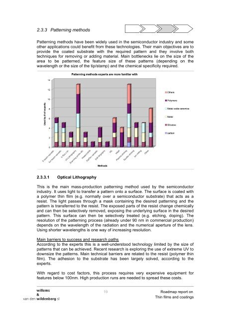
2.3.3 Patterning methods<br />
Patterning methods have been widely used in the semiconductor industry and some<br />
other applications could benefit from these technologies. Their main objectives are to<br />
provide the coated substrate with the required pattern and they involve both<br />
techniques for removing or adding material. Main bottlenecks lie on the size of the<br />
area to be patterned, the feature size of these patterns (depending on the<br />
wavelength or the size of the tip/stamp) and the chemical specificity required.<br />
2.3.3.1 Optical Lithography<br />
This is the main mass-production patterning method used by the semiconductor<br />
industry. It uses light to transfer a pattern onto a surface. The surface is coated with<br />
a polymer thin film (e.g. normally over a semiconductor substrate) that acts as a<br />
resist. The light passes through a mask containing the desired patterning and the<br />
pattern is transferred to the resist. The exposed parts of the resist change chemically<br />
and can then be selectively removed, exposing the underlying surface in the desired<br />
pattern. This surface can then be selectively treated (e.g. etching, doping). The<br />
resolution of the patterning process (already under 90 nm in commercial production)<br />
depends on the wavelength of the radiation and the numerical aperture of the lens.<br />
Using shorter wavelengths is one way of increasing resolution.<br />
Main barriers to success and research paths<br />
According to the experts this is a well-understood technology limited by the size of<br />
patterns that can be achieved. Recent research is exploring the use of extreme UV to<br />
downsize the patterns. Main technical barriers are related to the resist (polymer thin<br />
film). The adhesion to the substrate has been largely solved, according to the<br />
experts.<br />
With regard to cost factors, this process requires very expensive equipment for<br />
features below 100nm. High production runs are needed to spread these costs.<br />
19 <strong>Roadmap</strong> report on<br />
Thin <strong>films</strong> and coatings