Patch Antenna Design using MICROWAVE STUDIO 1 What is CST ...
Patch Antenna Design using MICROWAVE STUDIO 1 What is CST ...
Patch Antenna Design using MICROWAVE STUDIO 1 What is CST ...

You also want an ePaper? Increase the reach of your titles
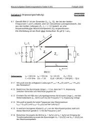
YUMPU automatically turns print PDFs into web optimized ePapers that Google loves.
<strong>Antenna</strong> Engineering, Peter Knott Tutorial <strong>Patch</strong> <strong>Antenna</strong> <strong>Design</strong><br />
<strong>Patch</strong> <strong>Antenna</strong> <strong>Design</strong> <strong>using</strong> <strong>MICROWAVE</strong> <strong>STUDIO</strong><br />
1 <strong>What</strong> <strong>is</strong> <strong>CST</strong> <strong>MICROWAVE</strong> <strong>STUDIO</strong> ?<br />
<strong>CST</strong> <strong>MICROWAVE</strong> <strong>STUDIO</strong> <strong>is</strong> a full-featured software package for electromagnetic analys<strong>is</strong><br />
and design in the high frequency range. It simplifies the process of inputting the structure<br />
by providing a powerful solid 3D modelling front end, see figure ??. Strong graphic<br />
feedback simplifies the definition of your device even further. After the component has<br />
been modelled, a fully automatic meshing procedure <strong>is</strong> applied before a simulation engine<br />
<strong>is</strong> started.<br />
<strong>CST</strong> <strong>MICROWAVE</strong> <strong>STUDIO</strong> <strong>is</strong> part of the <strong>CST</strong> DESIGN <strong>STUDIO</strong> suite [?] and offers<br />
a number of different solvers for different types of application. Since no method works<br />
equally well in all application domains, the software contains four different simulation<br />
techniques (transient solver, frequency domain solver, integral equation solver, eigenmode<br />
solver) to best fit their particular applications.<br />
The most flexible tool <strong>is</strong> the transient solver, which can obtain the entire broadband<br />
frequency behaviour of the simulated device from only one calculation run (in contrast<br />
to the frequency step approach of many other simulators). It <strong>is</strong> based on the Finite<br />
Integration Technique (FIT) introduced in electrodynamics more than three decades ago<br />
[?]. Th<strong>is</strong> solver <strong>is</strong> efficient for most kinds of high frequency applications such as connectors,<br />
transm<strong>is</strong>sion lines, filters, antennas and more. In th<strong>is</strong> tutorial we will make use of the<br />
transient solver for designing a microstrip patch antenna as an example.<br />
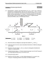
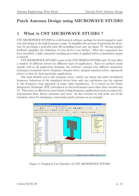
Figure 3: Graphical User Interface of <strong>CST</strong> <strong>MICROWAVE</strong> <strong>STUDIO</strong><br />
version 02/01/10 p. 11
<strong>Antenna</strong> Engineering, Peter Knott Tutorial <strong>Patch</strong> <strong>Antenna</strong> <strong>Design</strong><br />
2 Simulation Workflow<br />
After starting <strong>CST</strong> DESIGN ENVIRONMENT, choose to create a new <strong>CST</strong> <strong>MICROWAVE</strong><br />
<strong>STUDIO</strong> project. You will be asked to select a template for a structure which <strong>is</strong> closest<br />
to your device of interest, but you can also start from scratch opening an empty project.<br />
An interesting feature of the on-line help system <strong>is</strong> the Quick Start Guide, an electronic<br />
ass<strong>is</strong>tant that will guide you through your simulation. You can open th<strong>is</strong> ass<strong>is</strong>tant by<br />
selecting Help→Quick Start Guide if it does not show up automatically.<br />
If you are unsure of how to access a certain operation, click on the corresponding<br />
line. The Quick Start Guide will then either run an animation showing the location of<br />
the related menu entry or open the corresponding help page. As shown in the Quick<br />
Start-dialog box which should now be positioned in the upper right corner of the main<br />
view, the following steps have to be accompl<strong>is</strong>hed for a successful simulation:<br />
• Define the Units<br />
Choose the settings which make defining the dimensions, frequencies and time steps<br />
for your problem most comfortable. The defaults for th<strong>is</strong> structure type are geometrical<br />
lengths in mm and frequencies in GHz.<br />
• Define the Background Material<br />
By default, the modelled structure will be described within a perfectly conducting<br />
world. For an antenna problem, these settings have to be modified because the<br />
structure typically radiates in an unbounded (“open”) space or half-space. In order<br />
to change these settings, you can make changes in the corresponding dialogue box<br />
(Solve→Background Material).<br />
• Model the Structure<br />
Now the actual antenna structure has to be built. For modelling the antenna structure,<br />
a number of different geometrical design tools for typical geometries such<br />
as plates, cylinders, spheres etc. are provided in the CAD section of <strong>CST</strong> MI-<br />
CROWAVE <strong>STUDIO</strong>. These shapes can be added or intersected <strong>using</strong> boolean operators<br />
to build up more complex shapes. An overview of the different methods<br />
available in the tool-set and their properties <strong>is</strong> included in the on-line help.<br />
• Define the Frequency Range<br />
The next setting for the simulation <strong>is</strong> the frequency range of interest. You can specify<br />
the frequency by choosing Solve→Frequency from the main menu: Since you have<br />
already set the frequency units (to GHz for example), you need to define only the<br />
absolute numbers here (i.e. without units). The frequency settings are important<br />
because the mesh generator will adjust the mesh refinement (spatial sampling) to<br />
the frequency range specified.<br />
• Define Ports<br />
Every antenna structure needs a source of high-frequency energy for excitation of<br />
the desired electromagnetic waves. Structures may be excited e.g. <strong>using</strong> impressed<br />
currents or voltages between d<strong>is</strong>crete points or by wave-guide ports. The latter are<br />
pre-defined surfaces in which a limited number of eigenmodes are calculated and<br />
version 02/01/10 p. 12
<strong>Antenna</strong> Engineering, Peter Knott Tutorial <strong>Patch</strong> <strong>Antenna</strong> <strong>Design</strong><br />
may be stimulated. The correct definition of ports <strong>is</strong> very important for obtaining<br />
accurate S-parameters.<br />
• Define Boundary and Symmetry Conditions<br />
The simulation of th<strong>is</strong> structure will only be performed within the bounding box of<br />
the structure. You may, however, specify certain boundary conditions for each plane<br />
(x min , xmax, y min etc.) of the bounding box taking advantage of the symmetry in<br />
your specific problem. The boundary conditions are specified in a dialogue box that<br />
opens by choosing Solve→Boundary Conditions from the main menu.<br />
• Set Field Monitors<br />
In addition to the port impedance and S-parameters which are calculated automatically<br />
for each port, field quantities such as electric or magnetic currents, power flow,<br />
equivalent currents density or radiated far-field may be calculated. To invoke the<br />
calculation of these output data, use the command Solve→ Field Monitors.<br />
• Start the Simulation<br />
After defining all necessary parameters, you are ready to start your first simulation.<br />
Start the simulation from the transient solver control dialogue box: Solve→Transient<br />
Solver. In th<strong>is</strong> dialogue box, you can specify which column of the S-matrix should<br />
be calculated. Therefore, select the Source type port for which the couplings to all<br />
other ports will then be calculated during a single simulation run.<br />
2.1 Using Parameters<br />
<strong>CST</strong> <strong>MICROWAVE</strong> <strong>STUDIO</strong> has a built-in parametric optimizer that can help to find<br />
appropriate dimensions in your design. To take advantage of th<strong>is</strong> feature you need to<br />
declare one or more parameters in the parameter l<strong>is</strong>t (bottom left part of the program<br />
window) and use the symbols in almost every input field of the program (dimensions, port<br />
settings etc.) Also simple calculations <strong>using</strong> these pre-defined symbols are possible (e.g.<br />
4*x+y).<br />
3 Simulation Results<br />
After a successful simulation run, you will be able to access various calculation results<br />
and retrieve the obtained output data from the problem object tree at the right hand side<br />
of the program window.<br />
3.1 Analyse the Port Modes<br />
After the solver has completed the port mode calculation, you can view the results (even<br />
if the transient analys<strong>is</strong> <strong>is</strong> still running). In order to v<strong>is</strong>ualize a particular port mode, you<br />
must choose the solution from the navigation tree. If you open the specific sub-folder, you<br />
may select the electric or the magnetic mode field. Selecting the folder for the electric field<br />
of the first mode e1 will d<strong>is</strong>play the port mode and its relevant parameters in the main<br />
view: Besides information on the type of mode, you will also find the propagation constant<br />
version 02/01/10 p. 13
<strong>Antenna</strong> Engineering, Peter Knott Tutorial <strong>Patch</strong> <strong>Antenna</strong> <strong>Design</strong><br />
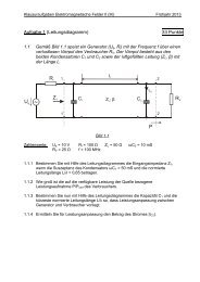
Figure 4: Typical <strong>Patch</strong> <strong>Antenna</strong> Geometry and Dimensions<br />
β at the central frequency. Additionally, the port impedance <strong>is</strong> calculated automatically<br />
(line impedance).<br />
3.2 Analyse S-Parameters and Field Quantities<br />
At the end of a successful simulation run you may also retrieve the other output data<br />
from the navigation tree, e.g. S-Parameters and electromagnetic field quantities.<br />
References<br />
[1] Computer Simulation Technology (<strong>CST</strong>), “<strong>CST</strong> <strong>Design</strong> Studio”,<br />
http://www.cst.com/Content/Products/DS/Overview.aspx<br />
[2] T. Weiland, “ D<strong>is</strong>cretization Method for the Solution of Maxwell’s Equations for<br />
Six-Component Fields”, Electron. Commun. (AEÜ), Vol. 31, No. 3, pp. 116-120,<br />
1977<br />
3.3 Exerc<strong>is</strong>es<br />
3.3.1 Rectangular <strong>Patch</strong> <strong>Antenna</strong> for WLAN application<br />
The aim of th<strong>is</strong> tutorial <strong>is</strong> the design of a microstrip patch antenna for a practical Wireless<br />
Local Area Network (WLAN) application operating at 2.4 GHz as well as connecting and<br />
matching the antenna to the system via a microstrip transm<strong>is</strong>sion line. The typical<br />
geometry of a patch antenna and the dimension parameters important for specifying a<br />
design are shown in figure ??.<br />
version 02/01/10 p. 14
<strong>Antenna</strong> Engineering, Peter Knott Tutorial <strong>Patch</strong> <strong>Antenna</strong> <strong>Design</strong><br />
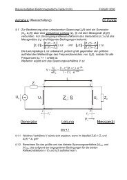
Figure 5: <strong>Antenna</strong> Matching Techniques: Asymmetric Feed, Recessed Feed and Quarter-<br />
Wavelength Transformer<br />
The antenna should be built on a dielectric substrate of industrial FR-4 material 1<br />
(ɛr = 4.9, µr = 1) of height hS = 1.0 mm. The PCB has a copper cladding of thickness<br />
hC = 35 µm on top and bottom. At the beginning, the substrate should be considered<br />
of infinite extent (open boundary conditions at the sides) and lossless, i.e. loss tangent<br />
tanδ = 0. Also the conductor material should be considered perfectly conducting (PEC).<br />
3.3.2 Coarse <strong>Design</strong><br />
The initial design should be a very simple microstrip-to-patch transition without any<br />
recesses or other impedance transformer (t = 0). Before you start modelling the antenna<br />
with <strong>CST</strong> <strong>MICROWAVE</strong> <strong>STUDIO</strong>, use the Transm<strong>is</strong>sion Line Model (TLM) design<br />
method illustrated in the script to calculate the approximate dimensions of the microstrip<br />
line width and patch width and height.<br />
3.3.3 <strong>CST</strong> Simulation<br />
Start <strong>CST</strong> <strong>MICROWAVE</strong> <strong>STUDIO</strong>, build a CAD model of the patch antenna (compr<strong>is</strong>ing<br />
feed line and rectangular patch on infinite PCB substrate) based on the approximated<br />
dimensions from the previous exerc<strong>is</strong>e and make the appropriate settings in the program<br />
for units, frequency, boundary conditions etc. If necessary, you can make use of the Quick<br />
Start Guide to lead you through the different steps.<br />
Use the transient solver to calculate the antenna properties. <strong>What</strong> are the resulting<br />
frequency of resonance and input reflection coefficient S11?<br />
3.3.4 Improved <strong>Antenna</strong> Matching<br />
Since the input impedance of the patch antenna <strong>is</strong> different from that of the feeding<br />
microstrip line, the m<strong>is</strong>match will cause a certain amount of reflected waves at the input<br />
port. With additional matching techniques (e.g. asymmetric feeding, recessed feed or<br />
quarter-wavelength transformer, see figure ??) you can reduce the m<strong>is</strong>match and improve<br />
reflection coefficient S11.<br />
Try out different matching techniques and see how you can improve antenna matching.<br />
<strong>What</strong> <strong>is</strong> the improvement of the 10 dB-bandwidth that you can achieve? Does it sat<strong>is</strong>fy the<br />
bandwidth requirements for operation in an IEEE 802.11b/g system (2.4 - 2.4835 GHz)?<br />
1 Flame Retardant 4, a glass reinforced epoxy laminate for manufacturing printed circuit boards<br />
version 02/01/10 p. 15
<strong>Antenna</strong> Engineering, Peter Knott Tutorial <strong>Patch</strong> <strong>Antenna</strong> <strong>Design</strong><br />
3.3.5 <strong>Antenna</strong> Far-field and Polar<strong>is</strong>ation<br />
Use a field monitor to calculate the far-field radiated by the antenna. <strong>What</strong> <strong>is</strong> the far-field<br />
polar<strong>is</strong>ation and maximum antenna gain in the direction normal to the antenna? How<br />
does changing the patch dimensions (W, L) affect these values?<br />
3.3.6 More Real<strong>is</strong>m<br />
For the sake of simplicity, some ideal<strong>is</strong>ed assumptions have been made in the previous<br />
design exerc<strong>is</strong>es (infinite and lossless substrate material). How do the results of the<br />
simulation change if<br />
a) the PCB has a finite size with a margin of 1 cm around the antenna and transm<strong>is</strong>sion<br />
line structure?<br />
b) the copper material <strong>is</strong> considered lossy (σ = 5.8 · 10 7 S/m)?<br />
3.3.7 Additional Exerc<strong>is</strong>es<br />
• <strong>Design</strong> a quadratic patch antenna with coaxial transm<strong>is</strong>sion line feed and two polarization<br />
ports.<br />
• <strong>Design</strong> a quadratic patch antenna with truncated edges for circular polar<strong>is</strong>ation.<br />
• <strong>Design</strong> an array cons<strong>is</strong>ting of 5 patch antennas with the beam scanned to 30 ◦ offboresight.<br />
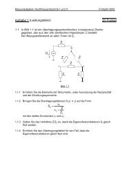
• <strong>Design</strong> an array of series fed patch antennas (see figure ??) for the same scanning<br />
direction.<br />
Figure 6: Series Fed <strong>Patch</strong> <strong>Antenna</strong> Array<br />
version 02/01/10 p. 16