High Voltage X7R Dielectric Product Bulletin - Kemet
High Voltage X7R Dielectric Product Bulletin - Kemet
High Voltage X7R Dielectric Product Bulletin - Kemet

Create successful ePaper yourself
Turn your PDF publications into a flip-book with our unique Google optimized e-Paper software.
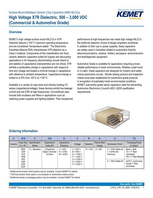
Surface Mount Multilayer Ceramic Chip Capacitors (SMD MLCCs)<br />
<strong>High</strong> <strong>Voltage</strong> <strong>X7R</strong> <strong>Dielectric</strong>, 500 – 3,000 VDC<br />
(Commercial & Automotive Grade)<br />
Overview<br />
KEMET’s high voltage surface mount MLCCs in <strong>X7R</strong><br />
<strong>Dielectric</strong> feature a 125°C maximum operating temperature<br />
and are considered “temperature stable.” The Electronics<br />
Industries Alliance (EIA) characterizes <strong>X7R</strong> dielectric as a<br />
Class II material. Components of this classification are fixed,<br />
ceramic dielectric capacitors suited for bypass and decoupling<br />
applications or for frequency discriminating circuits where Q<br />
and stability of capacitance characteristics are not critical. <strong>X7R</strong><br />
exhibits a predictable change in capacitance with respect to<br />
time and voltage and boasts a minimal change in capacitance<br />
with reference to ambient temperature. Capacitance change is<br />
limited to ±15% from -55°C to +125°C.<br />
Available in a variety of case sizes and industry leading CV<br />
values (capacitance/voltage), these devices exhibit low leakage<br />
current and low ESR at high frequencies. Conventional uses<br />
include both snubbers and filters in applications such as<br />
switching power supplies and lighting ballasts. Their exceptional<br />
performance at high frequencies has made high voltage MLCC's<br />
the preferred dielectric choice of design engineers worldwide.<br />
In addition to their use in power supplies, these capacitors<br />
are widely used in industries related to automotive (hybrid),<br />
telecommunications, medical, military, aerospace, semiconductors<br />
and test/diagnostic equipment.<br />
Automotive Grade is available for applications requiring proven,<br />
reliable performance in harsh environments. Whether under-hood<br />
or in-cabin, these capacitors are designed for mission and safety<br />
critical automotive circuits. Stricter testing protocol and inspection<br />
criteria have been established for automotive grade products<br />
in recognition of potentially harsh environmental conditions.<br />
KEMET automotive grade series capacitors meet the demanding<br />
Automotive Electronics Council's AEC–Q200 qualification<br />
requirements.<br />
Ordering Information<br />
C 1210 C 154 K C R A C TU<br />
Ceramic<br />
Case Size<br />
(L" x W")<br />
0805<br />
1206<br />
1210<br />
1808<br />
1812<br />
1825<br />
2220<br />
2225<br />
Specification/<br />
Series<br />
C = Standard<br />
Capacitance<br />
Code (pF)<br />
2 Significant<br />
Digits + Number<br />
of Zeros<br />
Capacitance<br />
Tolerance<br />
J = ±5%<br />
K = ±10%<br />
M = ±20%<br />
<strong>Voltage</strong> <strong>Dielectric</strong><br />
C = 500 V<br />
B = 630 V<br />
D = 1,000 V<br />
F = 1,500 V<br />
G = 2,000 V<br />
Z = 2,500 V<br />
H = 3,000 V<br />
1<br />
Additional termination finish options may be available. Contact KEMET for details.<br />
1, 2<br />
SnPb termination finish option is not available on Automotive Grade product.<br />
2<br />
Additional reeling or packaging options may be available. Contact KEMET for details.<br />
Failure Rate/<br />
Design<br />
Termination Finish 1<br />
R = <strong>X7R</strong> A = N/A C = 100% Matte Sn<br />
L = SnPb (5%<br />
minimum)<br />
C = 100% Matte Sn<br />
Packaging/Grade<br />
(C-Spec) 2<br />
Blank = Bulk<br />
TU = 7" Reel<br />
Unmarked<br />
TM = 7" Reel Marked<br />
AUTO = Automotive<br />
Grade 7" Reel<br />
Unmarked<br />
One world. One KEMET<br />
© KEMET Electronics Corporation • P.O. Box 5928 • Greenville, SC 29606 (864) 963-6300 • www.kemet.com C1010_<strong>X7R</strong>_HV_SMD • 6/18/2013 1
Surface Mount Multilayer Ceramic Chip Capacitors, (SMD MLCCs)<br />
<strong>High</strong> <strong>Voltage</strong> <strong>X7R</strong> <strong>Dielectric</strong>, 500 – 3,000 VDC (Commercial & Automotive Grade)<br />
Dimensions – Millimeters (Inches)<br />
W<br />
L<br />
T<br />
B<br />
S<br />
EIA<br />
Size<br />
Code<br />
Metric<br />
Size<br />
Code<br />
L<br />
Length<br />
W<br />
Width<br />
0805 2012 2.00 (.079) ± 0.20 (.008) 1.25 (.049) ± 0.20 (.008)<br />
T<br />
Thickness<br />
B<br />
Bandwidth<br />
S<br />
Separation<br />
Minimum<br />
0.50 (0.02) ± 0.25 (.010) 0.75 (.030)<br />
1206 3216 3.20 (.126) ± 0.20 (.008) 1.60 (.063) ± 0.20 (.008) 0.50 (0.02) ± 0.25 (.010)<br />
Mounting<br />
Technique<br />
Solder Wave or<br />
Solder Reflow<br />
1210 3225 3.20 (.126) ± 0.20 (.008) 2.50 (.098) ± 0.20 (.008) 0.50 (0.02) ± 0.25 (.010)<br />
1808 4520 4.70 (.185) ± 0.50 (.020) 2.00 (.079) ± 0.20 (.008)<br />
See Table 2 for<br />
0.60 (.024) ± 0.35 (.014)<br />
1812 4532 4.50 (.177) ± 0.30 (.012) 3.20 (.126) ± 0.30 (.012)<br />
Thickness<br />
0.60 (.024) ± 0.35 (.014)<br />
1825 4564 4.50 (.177) ± 0.30 (.012) 6.40 (.252) ± 0.40 (.016) 0.60 (.024) ± 0.35 (.014)<br />
N/A<br />
Solder Reflow Only<br />
2220 5650 5.70 (.224) ± 0.40 (.016) 5.00 (.197) ± 0.40 (.016) 0.60 (.024) ± 0.35 (.014)<br />
2225 5664 5.60 (.220) ± 0.40 (.016) 6.40 (.248) ± 0.40 (.016) 0.60 (.024) ± 0.35 (.014)<br />
Benefits<br />
• -55°C to +125°C operating temperature range<br />
• Industry-leading CV values<br />
• Exceptional performance at high frequencies<br />
• Pb-Free and RoHS Compliant<br />
• EIA 0805, 1206, 1210, 1808, 1812, 1825, 2220, and<br />
2225 case sizes<br />
• DC voltage ratings of 500 V, 630 V, 1 KV, 1.5 KV, 2 KV,<br />
2.5 KV, and 3 KV<br />
• Capacitance offerings ranging from 10 pF to 0.33 μF<br />
Ceramic Surface Mount<br />
• Available capacitance tolerances of ±5%, ±10%, and ±20%<br />
• Low ESR and ESL<br />
• Non-polar device, minimizing installation concerns<br />
• Commercial and Automotive (AEC–Q200) grades available<br />
• 100% pure matte tin-plated termination finish allowing for<br />
excellent solderability<br />
• SnPb plated termination finish option available upon request (5%<br />
minimum)<br />
Applications<br />
Typical applications include switch mode power supplies (input filters, resonators, tank circuits, snubber circuits, output filters), high<br />
voltage coupling and DC blocking, lighting ballasts, voltage multiplier circuits, DC/DC converters and coupling capacitors in Ćuk<br />
converters. Markets include power supply, LCD fluorescent backlight ballasts, HID lighting, telecom equipment, industrial and medical<br />
equipment/control, LAN/WAN interface, analog and digital modems, and automotive (electric and hybrid vehicles, charging stations and<br />
lighting) applications.<br />
© KEMET Electronics Corporation • P.O. Box 5928 • Greenville, SC 29606 (864) 963-6300 • www.kemet.com C1010_<strong>X7R</strong>_HV_SMD • 6/18/2013 2
Surface Mount Multilayer Ceramic Chip Capacitors, (SMD MLCCs)<br />
<strong>High</strong> <strong>Voltage</strong> <strong>X7R</strong> <strong>Dielectric</strong>, 500 – 3,000 VDC (Commercial & Automotive Grade)<br />
Application Note<br />
<strong>X7R</strong> dielectric is not recommended for AC line filtering or pulse applications.<br />
Qualification/Certification<br />
Commercial Grade products are subject to internal qualification. Details regarding test methods and conditions are referenced in<br />
Table 4, Performance & Reliability.<br />
Automotive Grade products meet or exceed the requirements outlined by the Automotive Electronics Council. Details regarding test<br />
methods and conditions are referenced in document AEC–Q200, Stress Test Qualification for Passive Components. For additional<br />
information regarding the Automotive Electronics Council and AEC–Q200, please visit their website at www.aecouncil.com.<br />
Environmental Compliance<br />
Pb-Free and RoHS Compliant (excluding SnPb termination finish option).<br />
Electrical Parameters/Characteristics<br />
Item<br />
Parameters/Characteristics<br />
Operating Temperature Range<br />
-55°C to +125°C<br />
Capacitance Change with Reference to +25°C and 0 VDC Applied (TCC) ±15%<br />
Aging Rate (Maximum % Capacitance Loss/Decade Hour) 3.0%<br />
<strong>Dielectric</strong> Withstanding <strong>Voltage</strong> (DWV)<br />
150% of rated voltage for voltage rating of < 1,000 V<br />
120% of rated voltage for voltage rating of ≥ 1,000 V<br />
(5 ±1 second and charge/discharge not exceeding 50 mA)<br />
Dissipation Factor (DF) Maximum Limit @ 25ºC 2.5%<br />
Insulation Resistance (IR) Limit @ 25°C<br />
See Insulation Resistance Limit Table<br />
(500 VDC applied for 120 ±5 seconds @ 25°C)<br />
Regarding aging rate: Capacitance measurements (including tolerance) are indexed to a referee time of 1,000 hours.<br />
To obtain IR limit, divide MΩ-µF value by the capacitance and compare to GΩ limit. Select the lower of the two limits.<br />
Capacitance and dissipation factor (DF) measured under the following conditions:<br />
1 kHz ±50 Hz and 1.0 ±0.2 Vrms if capacitance ≤ 10 µF<br />
120 Hz ±10 Hz and 0.5 ±0.1 Vrms if capacitance > 10 µF<br />
Note: When measuring capacitance it is important to ensure the set voltage level is held constant. The HP4284 and Agilent E4980 have a feature known as<br />
Automatic Level Control (ALC). The ALC feature should be switched to "ON."<br />
© KEMET Electronics Corporation • P.O. Box 5928 • Greenville, SC 29606 (864) 963-6300 • www.kemet.com C1010_<strong>X7R</strong>_HV_SMD • 6/18/2013 3
Surface Mount Multilayer Ceramic Chip Capacitors, (SMD MLCCs)<br />
<strong>High</strong> <strong>Voltage</strong> <strong>X7R</strong> <strong>Dielectric</strong>, 500 – 3,000 VDC (Commercial & Automotive Grade)<br />
Post Environmental Limits<br />
<strong>Dielectric</strong><br />
<strong>High</strong> Temperature Life, Biased Humidity, Moisture Resistance<br />
Rated DC<br />
<strong>Voltage</strong><br />
> 25<br />
Capacitance<br />
Value<br />
Dissipation Factor<br />
(Maximum %)<br />
3.0<br />
Capacitance<br />
Shift<br />
Insulation<br />
Resistance<br />
<strong>X7R</strong><br />
16/25 All<br />
5.0<br />
< 16 7.5<br />
±20% 10% of Initial Limit<br />
Insulation Resistance Limit Table (<strong>X7R</strong> <strong>Dielectric</strong>)<br />
EIA Case Size<br />
1,000 Megohm<br />
Microfarads or 100 GΩ<br />
100 Megohm<br />
Microfarads or 10 GΩ<br />
0805 < 0.0039 µF ≥ 0.0039 µF<br />
1206 < 0.012 µF ≥ 0.012 µF<br />
1210 < 0.033 µF ≥ 0.033 µF<br />
1808 < 0.018 µF ≥ 0.018 µF<br />
1812 < 0.027 µF ≥ 0.027 µF<br />
≥ 1825 All All<br />
© KEMET Electronics Corporation • P.O. Box 5928 • Greenville, SC 29606 (864) 963-6300 • www.kemet.com C1010_<strong>X7R</strong>_HV_SMD • 6/18/2013 4
Surface Mount Multilayer Ceramic Chip Capacitors, (SMD MLCCs)<br />
<strong>High</strong> <strong>Voltage</strong> <strong>X7R</strong> <strong>Dielectric</strong>, 500 – 3,000 VDC (Commercial & Automotive Grade)<br />
Table 1A – Capacitance Range/Selection Waterfall (0805 – 1812 Case Sizes)<br />
Capacitance<br />
Cap<br />
Code<br />
Series C0805 C1206 C1210 C1808 C1812<br />
<strong>Voltage</strong> Code C B D C B D F G C B D F G C B D F G Z H C B D F G Z H<br />
<strong>Voltage</strong> DC<br />
500<br />
630<br />
1000<br />
500<br />
630<br />
1000<br />
1500<br />
2000<br />
500<br />
Capacitance<br />
Tolerance<br />
<strong>Product</strong> Availability and Chip Thickness Codes - See Table 2 for Chip Thickness Dimensions<br />
10 pF 100 J K M DG DG DG EG EG EG EG EG FM FM FM FM FM LB LB LB LB LB LB LB GK GK GK GK GK GK GK<br />
11 pF 110 J K M DG DG DG EG EG EG EG EG FM FM FM FM FM LB LB LB LB LB LB LB GK GK GK GK GK GK GK<br />
12 pF 120 J K M DG DG DG EG EG EG EG EG FM FM FM FM FM LB LB LB LB LB LB LB GK GK GK GK GK GK GK<br />
13 pF 130 J K M DG DG DG EG EG EG EG EG FM FM FM FM FM LB LB LB LB LB LB LB GK GK GK GK GK GK GK<br />
15 pF 150 J K M DG DG DG EG EG EG EG EG FM FM FM FM FM LB LB LB LB LB LB LB GK GK GK GK GK GK GK<br />
16 pF 160 J K M DG DG DG EG EG EG EG EG FM FM FM FM FM LB LB LB LB LB LB LB GK GK GK GK GK GK GK<br />
18 pF 180 J K M DG DG DG EG EG EG EG EG FM FM FM FM FM LB LB LB LB LB LB LB GK GK GK GK GK GK GK<br />
20 pF 200 J K M DG DG DG EG EG EG EG EG FM FM FM FM FM LB LB LB LB LB LB LB GK GK GK GK GK GK GK<br />
22 pF 220 J K M DG DG DG EG EG EG EG EG FM FM FM FM FM LB LB LB LB LB LB LB GK GK GK GK GK GK GK<br />
24 pF 240 J K M DG DG DG EG EG EG EG EG FM FM FM FM FM LB LB LB LB LB LB LB GK GK GK GK GK GK GK<br />
27 pF 270 J K M DG DG DG EG EG EG EG EG FM FM FM FM FM LB LB LB LB LB LB LB GK GK GK GK GK GK GK<br />
30 pF 300 J K M DG DG DG EG EG EG EG EG FM FM FM FM FM LB LB LB LB LB LB LB GK GK GK GK GK GK GK<br />
33 pF 330 J K M DG DG DG EG EG EG EG EG FM FM FM FM FM LB LB LB LB LB LB LB GK GK GK GK GK GK GK<br />
36 pF 360 J K M DG DG DG EG EG EG EG EG FM FM FM FM FM LB LB LB LB LB LB LB GK GK GK GK GK GK GK<br />
39 pF 390 J K M DG DG DG EG EG EG EG EG FM FM FM FM FM LB LB LB LB LB LB LB GK GK GK GK GK GK GK<br />
43 pF 430 J K M DG DG DG EG EG EG EG EG FM FM FM FM FM LB LB LB LB LB LB LB GK GK GK GK GK GK GK<br />
47 pF 470 J K M DG DG DG EG EG EG EG EG FM FM FM FM FM LB LB LB LB LB LB LB GK GK GK GK GK GK GK<br />
51 pF 510 J K M DG DG DG EF EF EF EG EG FM FM FM FM FM LB LB LB LB LB LB LB GK GK GK GK GK GK GK<br />
56 pF 560 J K M DG DG DG EF EF EF EG EG FM FM FM FM FM LB LB LB LB LB LB LB GK GK GK GK GK GK GK<br />
62 pF 620 J K M DG DG DG EF EF EF EG EG FM FM FM FM FM LB LB LB LB LB LB LB GK GK GK GK GK GK GK<br />
68 pF 680 J K M DG DG DG EF EF EF EG EG FM FM FM FM FM LB LB LB LB LB LB LB GK GK GK GK GK GK GK<br />
75 pF 750 J K M DG DG DG EF EF EF EG EG FM FM FM FM FM LB LB LB LB LB LB LB GK GK GK GK GK GK GK<br />
82 pF 820 J K M DG DG DG EF EF EF EG EG FM FM FM FM FM LB LB LB LB LB LB LB GK GK GK GK GK GK GK<br />
91 pF 910 J K M DG DG DG EF EF EF EG EG FM FM FM FM FM LB LB LB LB LB LB LB GK GK GK GK GK GK GK<br />
100 pF 101 J K M DG DG DG EF EF EF EG EG FM FM FM FM FM LB LB LB LB LB LC LB GK GK GK GK GK GK GK<br />
110 pF 111 J K M DG DG DG EF EF EF EG EG FM FM FM FM FM LB LB LB LB LB LC LB GK GK GK GK GK GK GK<br />
120 pF 121 J K M DG DG DG EF EF EF EG EG FM FM FM FM FM LA LA LA LA LB LC LB GK GK GK GK GK GK GK<br />
130 pF 131 J K M DG DG DG EF EF EF EG EG FG FG FG FM FM LA LA LA LA LB LC LB GK GK GK GK GK GK GK<br />
150 pF 151 J K M DG DG DG EF EF EF EG EG FG FG FG FM FM LA LA LA LA LB LC LB GK GK GK GK GK GK GK<br />
180 pF 181 J K M DG DG DG EF EF EF EG EG FG FG FG FM FM LA LA LA LA LC LC LB GK GK GK GK GK GK GK<br />
220 pF 221 J K M DG DG DG EF EG EG EG EG FG FG FG FM FM LA LA LA LA LC LC LB GH GH GH GH GH GK GK<br />
270 pF 271 J K M DG DG DG EF EG EG EG EG FG FG FG FK FK LA LA LA LB LC LC LC GH GH GH GH GH GK GK<br />
330 pF 331 J K M DG DG DG EF EG EG EG EG FG FG FG FK FK LA LA LA LB LC LC LC GH GH GH GH GH GK GK<br />
390 pF 391 J K M DG DG DG EG EG EG EG EG FG FG FG FK FS LA LA LA LB LB LB LC GK GK GK GK GK GK GK<br />
470 pF 471 J K M DG DG DG EG EG EG EF EG FG FM FM FS FS LA LB LB LC LB LB LC GK GK GK GK GK GK GK<br />
560 pF 561 J K M DG DG DG EG EG EG EF EG FG FM FM FS FL LA LB LB LC LB LB LC GH GH GH GK GH GK GK<br />
680 pF 681 J K M DG DG DG EG EG EG EF EG FG FM FM FS FL LB LB LB LA LB LC LC GH GH GH GK GH GK GK<br />
820 pF 821 J K M DG DG DG EG EF EF EF EG FG FM FM FL FL LB LB LB LA LB LC LC GH GH GH GK GH GK GK<br />
1,000 pF 102 J K M DG DG DG EG EF EF EF EG FM FM FM FL FL LB LB LB LA LB LC LC GH GH GH GH GH GK GK<br />
1,200 pF 122 J K M DG DG DG EF EF EF EG EG FM FK FK FL FM LC LC LC LB LC LA GH GK GK GH GH GK GK<br />
1,500 pF 152 J K M DG DG DG EF EF EF EG EG FK FS FS FL FM LC LC LC LB LC LB GK GK GK GH GH GK<br />
1,800 pF 182 J K M DG DG DG EF EF EF EG EG FK FS FS FL FM LC LC LC LB LC LC GK GK GK GH GH GK<br />
2,000 pF 202 J K M DG DG DG EF EF EF EG EG FK FL FL FL FM LC LA LA LB LC LC GK GK GK GH GH GK<br />
2,200 pF 222 J K M DG DG DG EF EF EF EG EG FK FL FL FL FM LC LA LA LB LC LC GK GK GK GH GH GK<br />
2,700 pF 272 J K M DG DG DG EF EF EF EG FS FL FL FL FM LC LA LA LB LC GK GH GH GH GK GM<br />
3,300 pF 332 J K M DG DG DG EF EF EF EG FS FL FL FL FM LA LA LA LB LA GK GH GH GH GK GM<br />
3,900 pF 392 J K M DG DG DG EF EF EF EG FL FL FL FL FK LA LA LA LB LB GK GH GH GH GK GO<br />
4,700 pF 472 J K M DG DG DG EF EF EF EG FL FL FL FL FK LA LA LA LB LC GH GH GH GH GH GO<br />
5,600 pF 562 J K M DG DG EF EF EF EF FL FL FL FM FK LA LB LB LC GH GH GH GK GK<br />
6,800 pF 682 J K M DG DG EG EG EG EF FL FL FL FM FS LA LB LB LC GH GH GH GK GM<br />
8,200 pF 822 J K M DG DG EG EG EG EF FL FL FL FK LA LB LB LC GH GH GH GK GM<br />
10,000 pF 103 J K M DG EG EG EG EG FL FL FL FK LA LB LB LC GH GH GH GK GO<br />
12,000 pF 123 J K M DG EG EJ EJ FL FL FL FK LA LC LC LB GH GK GK GK<br />
Capacitance<br />
Cap<br />
Code<br />
<strong>Voltage</strong> DC<br />
500<br />
630<br />
1000<br />
500<br />
630<br />
1000<br />
1500<br />
2000<br />
500<br />
630<br />
630<br />
1000<br />
1000<br />
1500<br />
1500<br />
<strong>Voltage</strong> Code C B D C B D F G C B D F G C B D F G Z H C B D F G Z H<br />
Series C0805 C1206 C1210 C1808 C1812<br />
KEMET reserves the right to substitute product with an improved temperature characteristic, tighter capacitance tolerance and/or higher voltage capability within<br />
the same form factor (configuration and dimensions).<br />
2000<br />
2000<br />
500<br />
500<br />
630<br />
630<br />
1000<br />
1000<br />
1500<br />
1500<br />
2000<br />
2000<br />
2500<br />
2500<br />
3000<br />
3000<br />
500<br />
500<br />
630<br />
630<br />
1000<br />
1000<br />
1500<br />
1500<br />
2000<br />
2000<br />
2500<br />
2500<br />
3000<br />
3000<br />
© KEMET Electronics Corporation • P.O. Box 5928 • Greenville, SC 29606 (864) 963-6300 • www.kemet.com C1010_<strong>X7R</strong>_HV_SMD • 6/18/2013 5
Surface Mount Multilayer Ceramic Chip Capacitors, (SMD MLCCs)<br />
<strong>High</strong> <strong>Voltage</strong> <strong>X7R</strong> <strong>Dielectric</strong>, 500 – 3,000 VDC (Commercial & Automotive Grade)<br />
Table 1A – Capacitance Range/Selection Waterfall (0805 – 1812 Case Sizes) cont'd<br />
Capacitance<br />
Capacitance<br />
Cap<br />
Code<br />
Series C1825 C2220 C2225<br />
<strong>Voltage</strong> Code C B D F G Z H C B D F G Z H C B D F G Z H<br />
<strong>Voltage</strong> DC<br />
500<br />
630<br />
1000<br />
1500<br />
2000<br />
2500<br />
KEMET reserves the right to substitute product with an improved temperature characteristic, tighter capacitance tolerance and/or higher voltage capability within<br />
the same form factor (configuration and dimensions).<br />
3000<br />
Capacitance<br />
Tolerance<br />
<strong>Product</strong> Availability and Chip Thickness Codes – See Table 2 for Chip Thickness Dimensions<br />
100 pF 101 J K M HG HG HG HG HG HG HG JK JK JK JK JK JK JK KF KF KF KF KF KF KF<br />
110 pF 111 J K M HG HG HG HG HG HG HG JK JK JK JK JK JK JK KF KF KF KF KF KF KF<br />
120 pF 121 J K M HG HG HG HG HG HG HG JK JK JK JK JK JK JK KF KF KF KF KF KF KF<br />
130 pF 131 J K M HG HG HG HG HG HG HG JK JK JK JK JK JK JK KF KF KF KF KF KF KF<br />
150 pF 151 J K M HG HG HG HG HG HG HG JK JK JK JK JK JK JK KF KF KF KF KF KF KF<br />
180 pF 181 J K M HG HG HG HG HG HG HG JK JK JK JK JK JK JK KF KF KF KF KF KF KF<br />
220 pF 221 J K M HE HE HE HE HE HE HG JK JK JK JK JK JK JK KF KF KF KF KF KF KF<br />
270 pF 271 J K M HE HE HE HE HE HE HG JK JK JK JK JK JK JK KE KE KE KE KE KE KF<br />
330 pF 331 J K M JE JE JE JE JE JK JK KE KE KE KE KE KE KF<br />
390 pF 391 J K M JE JE JE JE JE JK JK KE KE KE KE KE KE KF<br />
470 pF 471 J K M HG HG HG HG HG HG HG JE JE JE JE JE JK JK KF KF KF KF KE KE KF<br />
560 pF 561 J K M HG HG HG HG HG HG HG JK JK JK JK JK JK JK KF KF KF KF KE KE KF<br />
680 pF 681 J K M HG HG HG HG HG HG HG JE JE JE JK JK JK JK KF KF KF KF KE KF KF<br />
820 pF 821 J K M HG HG HG HG HG HG HG JE JE JE JK JK JK JK KE KE KE KF KE KF KF<br />
1,000 pF 102 J K M HG HG HG HG HG HG HG JE JK JK JK JK JK JK KE KE KE KF KE KF KF<br />
1,200 pF 122 J K M HG HG HG HG HG HG HG JE JK JK JK JK JK JK KE KE KE KF KF KF KF<br />
1,500 pF 152 J K M HG HG HG HG HG HG HG JE JK JK JK JK JK JK KE KE KE KF KF KF KF<br />
1,800 pF 182 J K M HE HE HE HE HE HG HG JE JK JK JK JK JK JK KE KE KE KF KF KF KF<br />
Capacitance<br />
Cap<br />
Code<br />
Cap<br />
Code<br />
Series C0805 C1206 C1210 C1808 C1812<br />
<strong>Voltage</strong> Code C B D C B D F G C B D F G C B D F G Z H C B D F G Z H<br />
<strong>Voltage</strong> DC<br />
<strong>Voltage</strong> DC<br />
500<br />
500<br />
630<br />
1000<br />
630<br />
500<br />
1000<br />
630<br />
1500<br />
1000<br />
2000<br />
1500<br />
2000<br />
Capacitance<br />
Tolerance<br />
<strong>Product</strong> Availability and Chip Thickness Codes - See Table 2 for Chip Thickness Dimensions<br />
15,000 pF 153 J K M EG EJ EJ FL FL FL FL LA LC LC LC GH GK GK GH<br />
18,000 pF 183 J K M EJ EJ EJ FL FL FL FM LA LE LE GH GK GK GM<br />
22,000 pF 223 J K M EJ EJ EJ FL FM FM FM LA LE LE GH GK GK GM<br />
27,000 pF 273 J K M EJ EJ FM FK FK FK LA LA LA GH GB GB GO<br />
33,000 pF 333 J K M EJ EJ FM FG FH FS LC LA LA GH GB GB GO<br />
39,000 pF 393 J K M EJ FK FG FH FS LC LA LA GH GB GB<br />
47,000 pF 473 J K M EJ FK FH FK LC LA LB GH GB GC<br />
56,000 pF 563 J K M EJ FG FH FK LC LA LB GH GB GE<br />
62,000 pF 623 J K M EJ FG FK FS LA LA LC GK GB GE<br />
68,000 pF 683 J K M EJ FG FK FS LA LA LC GE GE GE<br />
82,000 pF 823 J K M FH FK LA LC GB GE GK<br />
0.10 µF 104 J K M FK FS LA LC GB GH GJ<br />
0.12 µF 124 J K M FK LA GE GK<br />
0.15 µF 154 J K M FK LB GE GN<br />
0.18 µF 184 J K M GF<br />
0.22 µF 224 J K M GJ<br />
0.27 µF 274 J K M GL<br />
0.33 µF 334 J K M GS<br />
Capacitance<br />
Cap<br />
Code<br />
<strong>Voltage</strong> DC<br />
500<br />
630<br />
1000<br />
500<br />
630<br />
1000<br />
1500<br />
2000<br />
2500<br />
500<br />
500<br />
3000<br />
630<br />
630<br />
500<br />
500<br />
1000<br />
1000<br />
630<br />
630<br />
1500<br />
1500<br />
<strong>Voltage</strong> Code C B D C B D F G C B D F G C B D F G Z H C B D F G Z H<br />
Series C0805 C1206 C1210 C1808 C1812<br />
Table 1B – Capacitance Range/Selection Waterfall (1825–2225 Case Sizes)<br />
<strong>Voltage</strong> Code C B D F G Z H C B D F G Z H C B D F G Z H<br />
Series C1825 C2220 C2225<br />
2000<br />
2000<br />
1000<br />
1000<br />
500<br />
500<br />
1500<br />
1500<br />
630<br />
630<br />
2000<br />
2000<br />
1000<br />
1000<br />
1500<br />
1500<br />
2500<br />
2500<br />
2000<br />
2000<br />
3000<br />
3000<br />
2500<br />
2500<br />
500<br />
500<br />
3000<br />
3000<br />
630<br />
630<br />
500<br />
500<br />
630<br />
630<br />
1000<br />
1000<br />
1000<br />
1000<br />
1500<br />
1500<br />
1500<br />
1500<br />
2000<br />
2000<br />
2000<br />
2000<br />
2500<br />
2500<br />
2500<br />
2500<br />
3000<br />
3000<br />
3000<br />
3000<br />
© KEMET Electronics Corporation • P.O. Box 5928 • Greenville, SC 29606 (864) 963-6300 • www.kemet.com C1010_<strong>X7R</strong>_HV_SMD • 6/18/2013 6
Surface Mount Multilayer Ceramic Chip Capacitors, (SMD MLCCs)<br />
<strong>High</strong> <strong>Voltage</strong> <strong>X7R</strong> <strong>Dielectric</strong>, 500 – 3,000 VDC (Commercial & Automotive Grade)<br />
Table 1B – Capacitance Range/Selection Waterfall (1825 – 2225 Case Sizes) cont'd<br />
Capacitance<br />
Cap<br />
Code<br />
Series C1825 C2220 C2225<br />
<strong>Voltage</strong> Code C B D F G Z H C B D F G Z H C B D F G Z H<br />
<strong>Voltage</strong> DC<br />
500<br />
630<br />
1000<br />
1500<br />
2000<br />
2500<br />
3000<br />
Capacitance<br />
Tolerance<br />
<strong>Product</strong> Availability and Chip Thickness Codes – See Table 2 for Chip Thickness Dimensions<br />
2,000 pF 202 J K M HE HE HE HE HE HG HG JE JK JK JE JE JK JK KE KE KE KF KF KF KF<br />
2,200 pF 222 J K M HE HE HE HE HE HG HG JE JK JK JE JE JK JK KF KE KE KF KF KF KF<br />
2,700 pF 272 J K M HE HE HE HE HE HG JK JK JK JE JE JK JK KE KE KE KE KE KF KE<br />
3,300 pF 332 J K M HE HE HE HE HE HG JK JK JK JE JE JK JE KE KE KE KE KE KF KE<br />
3,900 pF 392 J K M HE HE HE HE HE HG JK JK JK JE JE JK JE KE KF KF KE KE KF KE<br />
4,700 pF 472 J K M HE HE HE HE HE HG JK JK JK JE JK JE JE KE KF KF KE KE KF KE<br />
5,600 pF 562 J K M HE HE HE HE HE HG JK JK JK JE JK JE JE KE KF KF KE KE KF KE<br />
6,800 pF 682 J K M HE HE HE HE HE HJ JK JE JE JE JK JE JE KE KF KF KE KF KE KE<br />
8,200 pF 822 J K M HE HE HE HE HE HJ JK JE JE JE JK JK JK KF KE KE KE KF KF KF<br />
10,000 pF 103 J K M HE HE HE HE HJ HK JE JE JE JE JL JL JL KF KE KE KE KF KH KH<br />
12,000 pF 123 J K M HE HE HE HG HJ JE JK JK JK JL JL JL KE KE KE KE KF KH KH<br />
15,000 pF 153 J K M HE HE HE HG HK JE JK JK JK JL JN JN KE KE KE KE KF KJ KJ<br />
18,000 pF 183 J K M HE HE HE HG JE JK JK JK JN KE KE KE KE KH<br />
22,000 pF 223 J K M HE HG HG HG JE JK JK JK JN KE KF KF KF KJ<br />
27,000 pF 273 J K M HE HG HG HG JE JK JK JK KE KF KF KF KJ<br />
33,000 pF 333 J K M HE HG HG HE JE JK JK JK KE KF KF KF<br />
39,000 pF 393 J K M HE HG HG HG JE JK JK JE KE KF KF KF<br />
47,000 pF 473 J K M HE HG HG HJ JE JK JK JK KE KF KF KF<br />
56,000 pF 563 J K M HE HG HG HJ JE JE JE JL KE KF KF KF<br />
62,000 pF 623 J K M HG HG HG HK JE JE JE JL KE KF KF KH<br />
68,000 pF 683 J K M HG HJ HJ HK JE JK JK JL KE KF KF KJ<br />
82,000 pF 823 J K M HG HJ HJ JE JL JL JN KE KF KF KJ<br />
0.10 µF 104 J K M HG HK HK JE JN JN KE KH KH KJ<br />
0.12 µF 124 J K M HG JE JN JN KE KH KH<br />
0.15 µF 154 J K M HG JK KF KJ KJ<br />
0.18 µF 184 J K M HG JK KF<br />
0.22 µF 224 J K M HG KF<br />
0.27 µF 274 J K M<br />
0.33 µF 334 J K M<br />
0.39 µF 394 J K M<br />
0.47 µF 474 J K M<br />
0.56 µF 564 J K M<br />
0.68 µF 684 J K M<br />
0.82 µF 824 J K M<br />
1.0 µF 105 J K M<br />
1.2 µF 125 J K M<br />
500<br />
630<br />
1000<br />
1500<br />
2000<br />
2500<br />
3000<br />
500<br />
630<br />
1000<br />
1500<br />
2000<br />
2500<br />
3000<br />
Capacitance<br />
Cap<br />
Code<br />
<strong>Voltage</strong> DC<br />
500<br />
630<br />
1000<br />
1500<br />
2000<br />
2500<br />
3000<br />
500<br />
630<br />
1000<br />
1500<br />
2000<br />
2500<br />
3000<br />
500<br />
630<br />
1000<br />
1500<br />
2000<br />
2500<br />
3000<br />
<strong>Voltage</strong> Code C B D F G Z H C B D F G Z H C B D F G Z H<br />
Series C1825 C2220 C2225<br />
KEMET reserves the right to substitute product with an improved temperature characteristic, tighter capacitance tolerance and/or higher voltage capability within<br />
the same form factor (configuration and dimensions).<br />
© KEMET Electronics Corporation • P.O. Box 5928 • Greenville, SC 29606 (864) 963-6300 • www.kemet.com C1010_<strong>X7R</strong>_HV_SMD • 6/18/2013 7
Surface Mount Multilayer Ceramic Chip Capacitors, (SMD MLCCs)<br />
<strong>High</strong> <strong>Voltage</strong> <strong>X7R</strong> <strong>Dielectric</strong>, 500 – 3,000 VDC (Commercial & Automotive Grade)<br />
Table 2 – Chip Thickness/Packaging Quantities<br />
Thickness<br />
Code<br />
Case<br />
Size<br />
Thickness ±<br />
Range (mm)<br />
Paper Quantity<br />
Plastic Quantity<br />
7" Reel 13" Reel 7" Reel 13" Reel<br />
DG 0805 1.25 ± 0.15 0 0 2,500 10,000<br />
EF 1206 1.20 ± 0.15 0 0 2,500 10,000<br />
EG 1206 1.60 ± 0.15 0 0 2,000 8,000<br />
EJ 1206 1.70 ± 0.20 0 0 2,000 8,000<br />
FG 1210 1.25 ± 0.15 0 0 2,500 10,000<br />
FL 1210 1.40 ± 0.15 0 0 2,000 8,000<br />
FH 1210 1.55 ± 0.15 0 0 2,000 8,000<br />
FM 1210 1.70 ± 0.20 0 0 2,000 8,000<br />
FK 1210 2.10 ± 0.20 0 0 2,000 8,000<br />
FS 1210 2.50 ± 0.20 0 0 1,000 4,000<br />
LE 1808 1.00 ± 0.10 0 0 2,500 10,000<br />
LA 1808 1.40 ± 0.15 0 0 1,000 4,000<br />
LB 1808 1.60 ± 0.15 0 0 1,000 4,000<br />
LC 1808 2.00 ± 0.15 0 0 1,000 4,000<br />
GB 1812 1.00 ± 0.10 0 0 1,000 4,000<br />
GC 1812 1.10 ± 0.10 0 0 1,000 4,000<br />
GE 1812 1.30 ± 0.10 0 0 1,000 4,000<br />
GH 1812 1.40 ± 0.15 0 0 1,000 4,000<br />
GF 1812 1.50 ± 0.10 0 0 1,000 4,000<br />
GK 1812 1.60 ± 0.20 0 0 1,000 4,000<br />
GJ 1812 1.70 ± 0.15 0 0 1,000 4,000<br />
GN 1812 1.70 ± 0.20 0 0 1,000 4,000<br />
GL 1812 1.90 ± 0.20 0 0 500 2,000<br />
GM 1812 2.00 ± 0.20 0 0 500 2,000<br />
GS 1812 2.10 ± 0.20 0 0 500 2,000<br />
GO 1812 2.50 ± 0.20 0 0 500 2,000<br />
HE 1825 1.40 ± 0.15 0 0 1,000 4,000<br />
HG 1825 1.60 ± 0.20 0 0 1,000 4,000<br />
HJ 1825 2.00 ± 0.20 0 0 500 2,000<br />
HK 1825 2.50 ± 0.20 0 0 500 2,000<br />
JE 2220 1.40 ± 0.15 0 0 1,000 4,000<br />
JK 2220 1.60 ± 0.20 0 0 500 2,000<br />
JL 2220 2.00 ± 0.20 0 0 500 2,000<br />
JN 2220 2.50 ± 0.20 0 0 500 2,000<br />
KE 2225 1.40 ± 0.15 0 0 1,000 4,000<br />
KF 2225 1.60 ± 0.20 0 0 1,000 4,000<br />
KH 2225 2.00 ± 0.20 0 0 500 2,000<br />
KJ 2225 2.50 ± 0.20 0 0 500 2,000<br />
Thickness<br />
Code<br />
Case<br />
Size<br />
Thickness ±<br />
Range (mm)<br />
Package quantity based on finished chip thickness specifications.<br />
7" Reel 13" Reel 7" Reel 13" Reel<br />
Paper Quantity<br />
Plastic Quantity<br />
© KEMET Electronics Corporation • P.O. Box 5928 • Greenville, SC 29606 (864) 963-6300 • www.kemet.com C1010_<strong>X7R</strong>_HV_SMD • 6/18/2013 8
Surface Mount Multilayer Ceramic Chip Capacitors, (SMD MLCCs)<br />
<strong>High</strong> <strong>Voltage</strong> <strong>X7R</strong> <strong>Dielectric</strong>, 500 – 3,000 VDC (Commercial & Automotive Grade)<br />
Table 3 – Chip Capacitor Land Pattern Design Recommendations per IPC–7351<br />
EIA<br />
Size<br />
Code<br />
Metric<br />
Size<br />
Code<br />
Density Level A:<br />
Maximum (Most)<br />
Land Protrusion (mm)<br />
Density Level B:<br />
Median (Nominal)<br />
Land Protrusion (mm)<br />
Density Level C:<br />
Minimum (Least)<br />
Land Protrusion (mm)<br />
C Y X V1 V2 C Y X V1 V2 C Y X V1 V2<br />
0805 2012 1.00 1.35 1.55 4.40 2.60 0.90 1.15 1.45 3.50 2.00 0.80 0.95 1.35 2.80 1.70<br />
1206 3216 1.60 1.65 1.90 5.90 2.90 1.50 1.45 1.80 5.00 2.30 1.40 1.25 1.70 4.30 2.00<br />
1210 3225 1.60 1.65 2.80 5.90 3.80 1.50 1.45 2.70 5.00 3.20 1.40 1.25 2.60 4.30 2.90<br />
1210 1 3225 1.50 1.60 2.90 5.60 3.90 1.40 1.40 2.80 4.70 3.30 1.30 1.20 2.70 4.00 3.00<br />
1808 4520 2.25 1.85 2.30 7.40 3.30 2.15 1.65 2.20 6.50 2.70 2.05 1.45 2.10 5.80 2.40<br />
1812 4532 2.10 1.80 3.60 7.00 4.60 2.00 1.60 3.50 6.10 4.00 1.90 1.40 3.40 5.40 3.70<br />
1825 4564 2.15 1.80 6.90 7.10 7.90 2.05 1.60 6.80 6.20 7.30 1.95 1.40 6.70 5.50 7.00<br />
2220 5650 2.85 2.10 5.50 8.80 6.50 2.75 1.90 5.40 7.90 5.90 2.65 1.70 5.30 7.20 5.60<br />
2225 5664 2.85 2.10 6.90 8.80 7.90 2.75 1.90 6.80 7.90 7.30 2.65 1.70 6.70 7.20 7.00<br />
1<br />
Only for capacitance values ≥ 22 µF<br />
Density Level A: For low-density product applications. Recommended for wave solder applications and provides a wider process window for reflow solder<br />
processes. KEMET only recommends wave soldering of EIA 0603, 0805 and 1206 case sizes.<br />
Density Level B: For products with a moderate level of component density. Provides a robust solder attachment condition for reflow solder processes.<br />
Density Level C: For high component density product applications. Before adapting the minimum land pattern variations the user should perform qualification<br />
testing based on the conditions outlined in IPC Standard 7351 (IPC–7351).<br />
Soldering Process<br />
Recommended Soldering Technique:<br />
• Solder wave or solder reflow for EIA case sizes 0603, 0805 and 1206<br />
• All other EIA case sizes are limited to solder reflow only<br />
Recommended Soldering Profile:<br />
• KEMET recommends following the guidelines outlined in IPC/JEDEC J–STD–020<br />
© KEMET Electronics Corporation • P.O. Box 5928 • Greenville, SC 29606 (864) 963-6300 • www.kemet.com C1010_<strong>X7R</strong>_HV_SMD • 6/18/2013 9
Surface Mount Multilayer Ceramic Chip Capacitors, (SMD MLCCs)<br />
<strong>High</strong> <strong>Voltage</strong> <strong>X7R</strong> <strong>Dielectric</strong>, 500 – 3,000 VDC (Commercial & Automotive Grade)<br />
Table 4 – Performance & Reliability: Test Methods and Conditions<br />
Stress Reference Test or Inspection Method<br />
Terminal Strength JIS–C–6429 Appendix 1, Note: Force of 1.8 kg for 60 seconds.<br />
Board Flex<br />
JIS–C–6429<br />
Appendix 2, Note: Standard termination system – 2.0 mm (minimum) for all except 3 mm for C0G.<br />
Flexible termination system – 3.0 mm (minimum).<br />
Magnification 50 X. Conditions:<br />
Solderability<br />
J–STD–002<br />
a) Method B, 4 hours @ 155°C, dry heat @ 235°C<br />
b) Method B @ 215°C category 3<br />
c) Method D, category 3 @ 260°C<br />
Temperature Cycling JESD22 Method JA–104 1,000 cycles (-55°C to +125°C). Measurement at 24 hours +/- 2 hours after test conclusion.<br />
Biased Humidity MIL–STD–202 Method 103<br />
Load Humidity: 1,000 hours 85°C/85% RH and 200 VDC maximum. Add 100 K ohm resistor.<br />
Measurement at 24 hours +/- 2 hours after test conclusion.<br />
Low Volt Humidity: 1,000 hours 85°C/85% RH and 1.5 V. Add 100 K ohm resistor. Measurement at<br />
24 hours +/- 2 hours after test conclusion.<br />
Moisture Resistance MIL–STD–202 Method 106<br />
t = 24 hours/cycle. Steps 7a and 7b not required. Unpowered. Measurement at 24 hours +/- 2 hours<br />
after test conclusion.<br />
Thermal Shock MIL–STD–202 Method 107<br />
-55°C/+125°C. Note: Number of cycles required – 300. Maximum transfer time – 20 seconds. Dwell<br />
time – 15 minutes. Air – Air.<br />
<strong>High</strong> Temperature Life MIL–STD–202 Method 108 1,000 hours at 125°C (85°C for X5R, Z5U and Y5V) with rated voltage applied.<br />
Storage Life MIL–STD–202 Method 108 150°C, 0 VDC for 1,000 hours.<br />
Vibration MIL–STD–202 Method 204<br />
5 g's for 20 minutes, 12 cycles each of 3 orientations. Note: Use 8" X 5" PCB 0.031" thick, 7 secure<br />
points on one long side and 2 secure points at corners of opposite sides. Parts mounted within 2"<br />
from any secure point. Test from 10 – 2,000 Hz.<br />
Mechanical Shock MIL–STD–202 Method 213 Figure 1 of Method 213, Condition F.<br />
Resistance to Solvents MIL–STD–202 Method 215 Add aqueous wash chemical, OKEM Clean or equivalent.<br />
Storage and Handling<br />
Ceramic chip capacitors should be stored in normal working environments. While the chips themselves are quite robust in other<br />
environments, solderability will be degraded by exposure to high temperatures, high humidity, corrosive atmospheres, and long term<br />
storage. In addition, packaging materials will be degraded by high temperature– reels may soften or warp and tape peel force may<br />
increase. KEMET recommends that maximum storage temperature not exceed 40ºC and maximum storage humidity not exceed 70%<br />
relative humidity. Temperature fluctuations should be minimized to avoid condensation on the parts and atmospheres should be free of<br />
chlorine and sulfur bearing compounds. For optimized solderability chip stock should be used promptly, preferably within 1.5 years of<br />
receipt.<br />
© KEMET Electronics Corporation • P.O. Box 5928 • Greenville, SC 29606 (864) 963-6300 • www.kemet.com C1010_<strong>X7R</strong>_HV_SMD • 6/18/2013 10
Surface Mount Multilayer Ceramic Chip Capacitors, (SMD MLCCs)<br />
<strong>High</strong> <strong>Voltage</strong> <strong>X7R</strong> <strong>Dielectric</strong>, 500 – 3,000 VDC (Commercial & Automotive Grade)<br />
Construction<br />
Reference Item Material<br />
A<br />
Finish 100% Matte Sn SnPb (5% min)<br />
B<br />
Termination<br />
System<br />
Barrier Layer Ni<br />
D Base Metal Cu<br />
E Inner Electrode Ni<br />
F <strong>Dielectric</strong> Material BaTiO 3<br />
Note: Image is exaggerated in order to clearly identify all components of construction.<br />
© KEMET Electronics Corporation • P.O. Box 5928 • Greenville, SC 29606 (864) 963-6300 • www.kemet.com C1010_<strong>X7R</strong>_HV_SMD • 6/18/2013 11
Surface Mount Multilayer Ceramic Chip Capacitors, (SMD MLCCs)<br />
<strong>High</strong> <strong>Voltage</strong> <strong>X7R</strong> <strong>Dielectric</strong>, 500 – 3,000 VDC (Commercial & Automotive Grade)<br />
Capacitor Marking (Optional):<br />
These surface mount multilayer ceramic capacitors are<br />
normally supplied unmarked. If required, they can be marked<br />
as an extra cost option. Marking is available on most KEMET<br />
devices but must be requested using the correct ordering<br />
code identifier(s). If this option is requested, two sides of the<br />
ceramic body will be laser marked with a “K” to identify KEMET,<br />
followed by two characters (per EIA–198 - see table below) to<br />
identify the capacitance value. EIA 0603 case size devices are<br />
limited to the “K” character only.<br />
Marking appears in legible contrast. Illustrated below is an<br />
example of an MLCC with laser marking of “KA8”, which<br />
designates a KEMET device with rated capacitance of 100 µF.<br />
Orientation of marking is vendor optional.<br />
_<br />
KA8<br />
Laser marking option is not available on:<br />
• C0G, Ultra Stable X8R and Y5V dielectric devices<br />
• EIA 0402 case size devices<br />
• EIA 0603 case size devices with Flexible Termination option.<br />
• KPS Commercial and Automotive Grade stacked devices.<br />
Capacitance (pF) For Various Alpha/Numeral Identifiers<br />
Numeral<br />
Alpha<br />
9 0 1 2 3 4 5 6 7 8<br />
Character<br />
Capacitance (pF)<br />
A 0.1 1 0 10 100 1,000 10,000 100,000 1,000,000 10,000,000 100,000,000<br />
B 0.11 1.1 11 110 1,100 11,000 110,000 1,100,000 11,000,000 110,000,000<br />
C 0.12 1 2 12 120 1,200 12,000 120,000 1,200,000 12,000,000 120,000,000<br />
D 0.13 1 3 13 130 1,300 13,000 130,000 1,300,000 13,000,000 130,000,000<br />
E 0.15 1 5 15 150 1,500 15,000 150,000 1,500,000 15,000,000 150,000,000<br />
F 0.16 1 6 16 160 1,600 16,000 160,000 1,600,000 16,000,000 160,000,000<br />
G 0.18 1 8 18 180 1,800 18,000 180,000 1,800,000 18,000,000 180,000,000<br />
H 0.2 2 0 20 200 2,000 20,000 200,000 2,000,000 20,000,000 200,000,000<br />
J 0.22 2 2 22 220 2,200 22,000 220,000 2,200,000 22,000,000 220,000,000<br />
K 0.24 2.4 24 240 2,400 24,000 240,000 2,400,000 24,000,000 240,000,000<br />
L 0.27 2.7 27 270 2,700 27,000 270,000 2,700,000 27,000,000 270,000,000<br />
M 0.3 3 0 30 300 3,000 30,000 300,000 3,000,000 30,000,000 300,000,000<br />
N 0.33 3 3 33 330 3,300 33,000 330,000 3,300,000 33,000,000 330,000,000<br />
P 0.36 3 6 36 360 3,600 36,000 360,000 3,600,000 36,000,000 360,000,000<br />
Q 0.39 3 9 39 390 3,900 39,000 390,000 3,900,000 39,000,000 390,000,000<br />
R 0.43 4 3 43 430 4,300 43,000 430,000 4,300,000 43,000,000 430,000,000<br />
S 0.47 4.7 47 470 4,700 47,000 470,000 4,700,000 47,000,000 470,000,000<br />
T 0.51 5.1 51 510 5,100 51,000 510,000 5,100,000 51,000,000 510,000,000<br />
U 0.56 5 6 56 560 5,600 56,000 560,000 5,600,000 56,000,000 560,000,000<br />
V 0.62 6 2 62 620 6,200 62,000 620,000 6,200,000 62,000,000 620,000,000<br />
W 0.68 6 8 68 680 6,800 68,000 680,000 6,800,000 68,000,000 680,000,000<br />
X 0.75 7 5 75 750 7,500 75,000 750,000 7,500,000 75,000,000 750,000,000<br />
Y 0.82 8 2 82 820 8,200 82,000 820,000 8,200,000 82,000,000 820,000,000<br />
Z 0.91 9.1 91 910 9,100 91,000 910,000 9,100,000 91,000,000 910,000,000<br />
a 0.25 2 5 25 250 2,500 25,000 250,000 2,500,000 25,000,000 250,000,000<br />
b 0.35 3 5 35 350 3,500 35,000 350,000 3,500,000 35,000,000 350,000,000<br />
d 0.4 4 0 40 400 4,000 40,000 400,000 4,000,000 40,000,000 400,000,000<br />
e 0.45 4 5 45 450 4,500 45,000 450,000 4,500,000 45,000,000 450,000,000<br />
f 0.5 5 0 50 500 5,000 50,000 500,000 5,000,000 50,000,000 500,000,000<br />
m 0.6 6 0 60 600 6,000 60,000 600,000 6,000,000 60,000,000 600,000,000<br />
n 0.7 7 0 70 700 7,000 70,000 700,000 7,000,000 70,000,000 700,000,000<br />
t 0.8 8 0 80 800 8,000 80,000 800,000 8,000,000 80,000,000 800,000,000<br />
y 0.9 9 0 90 900 9,000 90,000 900,000 9,000,000 90,000,000 900,000,000<br />
© KEMET Electronics Corporation • P.O. Box 5928 • Greenville, SC 29606 (864) 963-6300 • www.kemet.com C1010_<strong>X7R</strong>_HV_SMD • 6/18/2013 12
Surface Mount Multilayer Ceramic Chip Capacitors, (SMD MLCCs)<br />
<strong>High</strong> <strong>Voltage</strong> <strong>X7R</strong> <strong>Dielectric</strong>, 500 – 3,000 VDC (Commercial & Automotive Grade)<br />
Tape & Reel Packaging Information<br />
KEMET offers multilayer ceramic chip capacitors packaged in 8, 12 and 16 mm tape on 7" and 13" reels in accordance with EIA<br />
Standard 481. This packaging system is compatible with all tape-fed automatic pick and place systems. See Table 2 for details on<br />
reeling quantities for commercial chips.<br />
Bar Code Label<br />
Anti-Static Reel<br />
KEMET ®<br />
Embossed Plastic* or<br />
Punched Paper Carrier.<br />
Chip and KPS Orientation in Pocket<br />
(except 1825 Commercial, and 1825 and 2225 Military)<br />
Sprocket Holes<br />
Embossment or Punched Cavity<br />
178 mm (7.00")<br />
or<br />
330 mm (13.00")<br />
8 mm, 12 mm<br />
or 16 mm Carrier Tape<br />
Anti-Static Cover Tape<br />
(.10 mm (.004") Maximum Thickness)<br />
*EIA 01005, 0201, 0402 and 0603 case sizes available on punched paper carrier only.<br />
Table 5 – Carrier Tape Configuration – Embossed Plastic & Punched Paper (mm)<br />
EIA Case Size Tape Size (W)* Pitch (P 1<br />
)*<br />
01005 – 0402 8 2<br />
0603 – 1210 8 4<br />
1805 – 1808 12 4<br />
≥ 1812 12 8<br />
KPS 1210 12 8<br />
KPS 1812 & 2220 16 12<br />
Array 0508 & 0612 8 4<br />
*Refer to Figures 1 & 2 for W and P 1<br />
carrier tape reference locations.<br />
*Refer to Tables 6 & 7 for tolerance specifications.<br />
© KEMET Electronics Corporation • P.O. Box 5928 • Greenville, SC 29606 (864) 963-6300 • www.kemet.com C1010_<strong>X7R</strong>_HV_SMD • 6/18/2013 13
Surface Mount Multilayer Ceramic Chip Capacitors, (SMD MLCCs)<br />
<strong>High</strong> <strong>Voltage</strong> <strong>X7R</strong> <strong>Dielectric</strong>, 500 – 3,000 VDC (Commercial & Automotive Grade)<br />
Figure 1 – Embossed (Plastic) Carrier Tape Dimensions<br />
T<br />
T2<br />
ØDo<br />
P2<br />
Po<br />
[10 pitches cumulative<br />
tolerance on tape ± 0.2 mm]<br />
E1<br />
Ao<br />
F<br />
B1<br />
Ko<br />
Bo<br />
E2<br />
W<br />
S1<br />
P1<br />
T1<br />
Cover Tape<br />
B1 is for tape feeder reference only,<br />
including draft concentric about B o.<br />
Center Lines of Cavity<br />
User Direction of Unreeling<br />
ØD1<br />
Embossment<br />
For cavity size,<br />
see Note 1 Table 4<br />
Table 6 – Embossed (Plastic) Carrier Tape Dimensions<br />
Metric will govern<br />
Constant Dimensions — Millimeters (Inches)<br />
Tape Size D 0<br />
8 mm<br />
12 mm<br />
16 mm<br />
1.5 +0.10/-0.0<br />
(0.059 +0.004/-0.0)<br />
D 1<br />
Minimum<br />
Note 1<br />
1.0<br />
(0.039)<br />
1.5<br />
(0.059)<br />
E 1<br />
P 0<br />
P 2<br />
1.75 ±0.10<br />
(0.069 ±0.004)<br />
4.0 ±0.10<br />
(0.157 ±0.004)<br />
2.0 ±0.05<br />
(0.079 ±0.002)<br />
R Reference<br />
Note 2<br />
25.0<br />
(0.984)<br />
30<br />
(1.181)<br />
S 1<br />
Minimum<br />
Note 3<br />
0.600<br />
(0.024)<br />
T<br />
Maximum<br />
0.600<br />
(0.024)<br />
T 1<br />
Maximum<br />
0.100<br />
(0.004)<br />
Variable Dimensions — Millimeters (Inches)<br />
Tape Size<br />
Pitch<br />
8 mm Single (4 mm)<br />
12 mm<br />
Single (4 mm) &<br />
Double (8 mm)<br />
16 mm Triple (12 mm)<br />
B 1<br />
Maximum<br />
Note 4<br />
4.35<br />
(0.171)<br />
8.2<br />
(0.323)<br />
12.1<br />
(0.476)<br />
E 2<br />
Minimum<br />
6.25<br />
(0.246)<br />
10.25<br />
(0.404)<br />
14.25<br />
(0.561)<br />
F P 1<br />
3.5 ±0.05<br />
(0.138 ±0.002)<br />
5.5 ±0.05<br />
(0.217 ±0.002)<br />
7.5 ±0.05<br />
(0.138 ±0.002)<br />
4.0 ±0.10<br />
(0.157 ±0.004)<br />
8.0 ±0.10<br />
(0.315 ±0.004)<br />
12.0 ±0.10<br />
(0.157 ±0.004)<br />
T 2<br />
Maximum<br />
2.5<br />
(0.098)<br />
4.6<br />
(0.181)<br />
4.6<br />
(0.181)<br />
W<br />
Maximum<br />
8.3<br />
(0.327)<br />
12.3<br />
(0.484)<br />
16.3<br />
(0.642)<br />
A 0<br />
,B 0<br />
& K 0<br />
Note 5<br />
1. The embossment hole location shall be measured from the sprocket hole controlling the location of the embossment. Dimensions of embossment location and<br />
hole location shall be applied independent of each other.<br />
2. The tape with or without components shall pass around R without damage (see Figure 6).<br />
3. If S 1<br />
< 1.0 mm, there may not be enough area for cover tape to be properly applied (see EIA Standard 481 paragraph 4.3 section b).<br />
4. B 1<br />
dimension is a reference dimension for tape feeder clearance only.<br />
5. The cavity defined by A 0<br />
, B 0<br />
and K 0<br />
shall surround the component with sufficient clearance that:<br />
(a) the component does not protrude above the top surface of the carrier tape.<br />
(b) the component can be removed from the cavity in a vertical direction without mechanical restriction, after the top cover tape has been removed.<br />
(c) rotation of the component is limited to 20° maximum for 8 and 12 mm tapes and 10° maximum for 16 mm tapes (see Figure 3).<br />
(d) lateral movement of the component is restricted to 0.5 mm maximum for 8 and 12 mm wide tape and to 1.0 mm maximum for 16 mm tape (see Figure 4).<br />
(e) for KPS Series product, A 0<br />
and B 0<br />
are measured on a plane 0.3 mm above the bottom of the pocket.<br />
(f) see Addendum in EIA Standard 481 for standards relating to more precise taping requirements.<br />
© KEMET Electronics Corporation • P.O. Box 5928 • Greenville, SC 29606 (864) 963-6300 • www.kemet.com C1010_<strong>X7R</strong>_HV_SMD • 6/18/2013 14
Surface Mount Multilayer Ceramic Chip Capacitors, (SMD MLCCs)<br />
<strong>High</strong> <strong>Voltage</strong> <strong>X7R</strong> <strong>Dielectric</strong>, 500 – 3,000 VDC (Commercial & Automotive Grade)<br />
Figure 2 – Punched (Paper) Carrier Tape Dimensions<br />
T<br />
ØDo<br />
P2<br />
Po<br />
[10 pitches cumulative<br />
tolerance on tape ± 0.2 mm]<br />
E1<br />
Bottom Cover Tape<br />
B0<br />
A0<br />
F<br />
E2<br />
W<br />
T1<br />
T1<br />
Top Cover Tape<br />
Center Lines of Cavity<br />
P1<br />
G<br />
Cavity Size,<br />
See<br />
Note 1, Table 7<br />
Bottom Cover Tape<br />
User Direction of Unreeling<br />
Table 7 – Punched (Paper) Carrier Tape Dimensions<br />
Metric will govern<br />
Constant Dimensions — Millimeters (Inches)<br />
Tape Size D 0<br />
E 1<br />
P 0<br />
P 2<br />
T 1<br />
Maximum G Minimum<br />
8 mm<br />
1.5 +0.10 -0.0<br />
(0.059 +0.004 -0.0)<br />
1.75 ±0.10<br />
(0.069 ±0.004)<br />
4.0 ±0.10<br />
(0.157 ±0.004)<br />
2.0 ±0.05<br />
(0.079 ±0.002)<br />
Variable Dimensions — Millimeters (Inches)<br />
0.10<br />
(0.004) Maximum<br />
0.75<br />
(0.030)<br />
R Reference<br />
Note 2<br />
25<br />
(0.984)<br />
Tape Size Pitch E2 Minimum F P 1<br />
T Maximum W Maximum A 0<br />
B 0<br />
8 mm Half (2 mm)<br />
2.0 ±0.05<br />
8.3<br />
6.25<br />
3.5 ±0.05 (0.079 ±0.002) 1.1<br />
(0.327)<br />
(0.246) (0.138 ±0.002)<br />
(0.098)<br />
Note 1<br />
8 mm Single (4 mm)<br />
4.0 ±0.10<br />
8.3<br />
(0.157 ±0.004)<br />
(0.327)<br />
1. The cavity defined by A 0<br />
, B 0<br />
and T shall surround the component with sufficient clearance that:<br />
a) the component does not protrude beyond either surface of the carrier tape.<br />
b) the component can be removed from the cavity in a vertical direction without mechanical restriction, after the top cover tape has been removed.<br />
c) rotation of the component is limited to 20° maximum (see Figure 3).<br />
d) lateral movement of the component is restricted to 0.5 mm maximum (see Figure 4).<br />
e) see Addendum in EIA Standard 481 for standards relating to more precise taping requirements.<br />
2. The tape with or without components shall pass around R without damage (see Figure 6).<br />
© KEMET Electronics Corporation • P.O. Box 5928 • Greenville, SC 29606 (864) 963-6300 • www.kemet.com C1010_<strong>X7R</strong>_HV_SMD • 6/18/2013 15
Surface Mount Multilayer Ceramic Chip Capacitors, (SMD MLCCs)<br />
<strong>High</strong> <strong>Voltage</strong> <strong>X7R</strong> <strong>Dielectric</strong>, 500 – 3,000 VDC (Commercial & Automotive Grade)<br />
Packaging Information Performance Notes<br />
1. Cover Tape Break Force: 1.0 Kg minimum.<br />
2. Cover Tape Peel Strength: The total peel strength of the cover tape from the carrier tape shall be:<br />
Tape Width<br />
Peel Strength<br />
8 mm 0.1 to 1.0 Newton (10 to 100 gf)<br />
12 and 16 mm 0.1 to 1.3 Newton (10 to 130 gf)<br />
The direction of the pull shall be opposite the direction of the carrier tape travel. The pull angle of the carrier tape shall be 165° to 180°<br />
from the plane of the carrier tape. During peeling, the carrier and/or cover tape shall be pulled at a velocity of 300 ±10 mm/minute.<br />
3. Labeling: Bar code labeling (standard or custom) shall be on the side of the reel opposite the sprocket holes. Refer to EIA<br />
Standards 556 and 624.<br />
Figure 3 – Maximum Component Rotation<br />
Bo<br />
°<br />
T<br />
Ao<br />
Maximum Component Rotation<br />
Top View<br />
Typical Pocket Centerline<br />
Maximum Component Rotation<br />
Side View<br />
Tape Maximum<br />
°<br />
°<br />
s<br />
Width (mm) Rotation ( T)<br />
8,12 20<br />
16 – 200 10 Tape Maximum<br />
Width (mm) Rotation (<br />
8,12 20<br />
Typical Component Centerline<br />
16 – 56 10<br />
72 – 200 5<br />
°<br />
S)<br />
Figure 4 – Maximum Lateral Movement<br />
Figure 5 – Bending Radius<br />
8 mm & 12 mm Tape<br />
0.5 mm maximum<br />
0.5 mm maximum<br />
16 mm Tape<br />
1.0 mm maximum<br />
1.0 mm maximum<br />
Embossed<br />
Carrier<br />
Punched<br />
Carrier<br />
R<br />
Bending<br />
Radius<br />
R<br />
© KEMET Electronics Corporation • P.O. Box 5928 • Greenville, SC 29606 (864) 963-6300 • www.kemet.com C1010_<strong>X7R</strong>_HV_SMD • 6/18/2013 16
Surface Mount Multilayer Ceramic Chip Capacitors, (SMD MLCCs)<br />
<strong>High</strong> <strong>Voltage</strong> <strong>X7R</strong> <strong>Dielectric</strong>, 500 – 3,000 VDC (Commercial & Automotive Grade)<br />
Figure 6 – Reel Dimensions<br />
Full Radius,<br />
See Note<br />
Access Hole at<br />
Slot Location<br />
(Ø 40 mm minimum)<br />
W3 (Includes<br />
flange distortion<br />
at outer edge)<br />
W2 (Measured at hub)<br />
A<br />
D (See Note)<br />
B (see Note)<br />
C<br />
(Arbor hole<br />
diameter)<br />
If present,<br />
tape slot in core<br />
for tape start:<br />
2.5 mm minimum width x<br />
10.0 mm minimum depth<br />
Note: Drive spokes optional; if used, dimensions B and D shall apply.<br />
N<br />
W1 (Measured at hub)<br />
Table 8 – Reel Dimensions<br />
Metric will govern<br />
Constant Dimensions — Millimeters (Inches)<br />
Tape Size A B Minimum C D Minimum<br />
8 mm 178 ±0.20<br />
(7.008 ±0.008)<br />
12 mm<br />
or<br />
330 ±0.20<br />
16 mm<br />
(13.000 ±0.008)<br />
1.5<br />
(0.059)<br />
Variable Dimensions — Millimeters (Inches)<br />
13.0 +0.5/-0.2<br />
(0.521 +0.02/-0.008)<br />
20.2<br />
(0.795)<br />
Tape Size N Minimum W 1<br />
W 2<br />
Maximum W 3<br />
8 mm<br />
8.4 +1.5/-0.0<br />
(0.331 +0.059/-0.0)<br />
14.4<br />
(0.567)<br />
12 mm<br />
50<br />
(1.969)<br />
12.4 +2.0/-0.0<br />
(0.488 +0.078/-0.0)<br />
18.4<br />
(0.724)<br />
Shall accommodate tape width<br />
without interference<br />
16 mm<br />
16.4 +2.0/-0.0<br />
(0.646 +0.078/-0.0)<br />
22.4<br />
(0.882)<br />
© KEMET Electronics Corporation • P.O. Box 5928 • Greenville, SC 29606 (864) 963-6300 • www.kemet.com C1010_<strong>X7R</strong>_HV_SMD • 6/18/2013 17
Surface Mount Multilayer Ceramic Chip Capacitors, (SMD MLCCs)<br />
<strong>High</strong> <strong>Voltage</strong> <strong>X7R</strong> <strong>Dielectric</strong>, 500 – 3,000 VDC (Commercial & Automotive Grade)<br />
Figure 7 – Tape Leader & Trailer Dimensions<br />
Embossed Carrier<br />
Punched Carrier<br />
8 mm & 12 mm only<br />
END<br />
Carrier Tape<br />
Round Sprocket Holes<br />
START<br />
Top Cover Tape<br />
Elongated Sprocket Holes<br />
(32 mm tape and wider)<br />
Trailer<br />
160 mm Minimum<br />
Top Cover Tape<br />
Components<br />
100 mm<br />
Minimum Leader<br />
400 mm Minimum<br />
Figure 8 – Maximum Camber<br />
Elongated sprocket holes<br />
(32 mm & wider tapes)<br />
Carrier Tape<br />
Round Sprocket Holes<br />
1 mm Maximum, either direction<br />
Straight Edge<br />
250 mm<br />
© KEMET Electronics Corporation • P.O. Box 5928 • Greenville, SC 29606 (864) 963-6300 • www.kemet.com C1010_<strong>X7R</strong>_HV_SMD • 6/18/2013 18
Surface Mount Multilayer Ceramic Chip Capacitors, (SMD MLCCs)<br />
<strong>High</strong> <strong>Voltage</strong> <strong>X7R</strong> <strong>Dielectric</strong>, 500 – 3,000 VDC (Commercial & Automotive Grade)<br />
KEMET Corporation<br />
World Headquarters<br />
2835 KEMET Way<br />
Simpsonville, SC 29681<br />
Mailing Address:<br />
P.O. Box 5928<br />
Greenville, SC 29606<br />
www.kemet.com<br />
Tel: 864-963-6300<br />
Fax: 864-963-6521<br />
Corporate Offices<br />
Fort Lauderdale, FL<br />
Tel: 954-766-2800<br />
North America<br />
Southeast<br />
Lake Mary, FL<br />
Tel: 407-855-8886<br />
Northeast<br />
Wilmington, MA<br />
Tel: 978-658-1663<br />
Central<br />
Novi, MI<br />
Tel: 248-994-1030<br />
West<br />
Milpitas, CA<br />
Tel: 408-433-9950<br />
Europe<br />
Southern Europe<br />
Paris, France<br />
Tel: 33-1-4646-1006<br />
Sasso Marconi, Italy<br />
Tel: 39-051-939111<br />
Central Europe<br />
Landsberg, Germany<br />
Tel: 49-8191-3350800<br />
Kamen, Germany<br />
Tel: 49-2307-438110<br />
Northern Europe<br />
Bishop’s Stortford, United Kingdom<br />
Tel: 44-1279-460122<br />
Espoo, Finland<br />
Tel: 358-9-5406-5000<br />
Asia<br />
Northeast Asia<br />
Hong Kong<br />
Tel: 852-2305-1168<br />
Shenzhen, China<br />
Tel: 86-755-2518-1306<br />
Beijing, China<br />
Tel: 86-10-5829-1711<br />
Shanghai, China<br />
Tel: 86-21-6447-0707<br />
Taipei, Taiwan<br />
Tel: 886-2-27528585<br />
Southeast Asia<br />
Singapore<br />
Tel: 65-6586-1900<br />
Penang, Malaysia<br />
Tel: 60-4-6430200<br />
Bangalore, India<br />
Tel: 91-806-53-76817<br />
Mexico<br />
Guadalajara, Jalisco<br />
Tel: 52-33-3123-2141<br />
Note: KEMET reserves the right to modify minor details of internal and external construction at any time in the interest of product improvement. KEMET does not<br />
assume any responsibility for infringement that might result from the use of KEMET Capacitors in potential circuit designs. KEMET is a registered trademark of<br />
KEMET Electronics Corporation.<br />
© KEMET Electronics Corporation • P.O. Box 5928 • Greenville, SC 29606 (864) 963-6300 • www.kemet.com C1010_<strong>X7R</strong>_HV_SMD • 6/18/2013 19
Surface Mount Multilayer Ceramic Chip Capacitors, (SMD MLCCs)<br />
<strong>High</strong> <strong>Voltage</strong> <strong>X7R</strong> <strong>Dielectric</strong>, 500 – 3,000 VDC (Commercial & Automotive Grade)<br />
Other KEMET Resources<br />
Tools<br />
Resource<br />
Configure A Part: CapEdge<br />
SPICE & FIT Software<br />
Search Our FAQs: KnowledgeEdge<br />
Electrolytic LifeCalculator<br />
http://capacitoredge.kemet.com<br />
http://www.kemet.com/spice<br />
http://www.kemet.com/keask<br />
http://www.kemet.com:8080/elc<br />
Location<br />
<strong>Product</strong> Information<br />
Resource<br />
<strong>Product</strong>s<br />
Technical Resources (Including Soldering Techniques)<br />
RoHS Statement<br />
Quality Documents<br />
Location<br />
http://www.kemet.com/products<br />
http://www.kemet.com/technicalpapers<br />
http://www.kemet.com/rohs<br />
http://www.kemet.com/qualitydocuments<br />
<strong>Product</strong> Request<br />
Resource<br />
Sample Request<br />
Engineering Kit Request<br />
http://www.kemet.com/sample<br />
http://www.kemet.com/kits<br />
Location<br />
Contact<br />
Resource<br />
Website<br />
Contact Us<br />
Investor Relations<br />
Call Us<br />
Twitter<br />
Location<br />
www.kemet.com<br />
http://www.kemet.com/contact<br />
http://www.kemet.com/ir<br />
1-877-MyKEMET<br />
http://twitter.com/kemetcapacitors<br />
Disclaimer<br />
All product specifications, statements, information and data (collectively, the “Information”) in this datasheet are subject to change. The customer is responsible for checking and<br />
verifying the extent to which the Information contained in this publication is applicable to an order at the time the order is placed.<br />
All Information given herein is believed to be accurate and reliable, but it is presented without guarantee, warranty, or responsibility of any kind, expressed or implied.<br />
Statements of suitability for certain applications are based on KEMET Electronics Corporation’s (“KEMET”) knowledge of typical operating conditions for such applications, but are<br />
not intended to constitute – and KEMET specifically disclaims – any warranty concerning suitability for a specific customer application or use. The Information is intended for use only<br />
by customers who have the requisite experience and capability to determine the correct products for their application. Any technical advice inferred from this Information or otherwise<br />
provided by KEMET with reference to the use of KEMET’s products is given gratis, and KEMET assumes no obligation or liability for the advice given or results obtained.<br />
Although KEMET designs and manufactures its products to the most stringent quality and safety standards, given the current state of the art, isolated component failures may still<br />
occur. Accordingly, customer applications which require a high degree of reliability or safety should employ suitable designs or other safeguards (such as installation of protective<br />
circuitry or redundancies) in order to ensure that the failure of an electrical component does not result in a risk of personal injury or property damage.<br />
Although all product–related warnings, cautions and notes must be observed, the customer should not assume that all safety measures are indicted or that other measures may not<br />
be required.<br />
© KEMET Electronics Corporation • P.O. Box 5928 • Greenville, SC 29606 (864) 963-6300 • www.kemet.com C1010_<strong>X7R</strong>_HV_SMD • 6/18/2013 20
Surface Mount Multilayer Ceramic Chip Capacitors, (SMD MLCCs)<br />
<strong>High</strong> <strong>Voltage</strong> <strong>X7R</strong> <strong>Dielectric</strong>, 500 – 3,000 VDC (Commercial & Automotive Grade)<br />
© KEMET Electronics Corporation • P.O. Box 5928 • Greenville, SC 29606 (864) 963-6300 • www.kemet.com C1010_<strong>X7R</strong>_HV_SMD • 6/18/2013 21