Annual Report 2011 / 2012 - E21 - Technische Universität München
Annual Report 2011 / 2012 - E21 - Technische Universität München
Annual Report 2011 / 2012 - E21 - Technische Universität München

Create successful ePaper yourself
Turn your PDF publications into a flip-book with our unique Google optimized e-Paper software.
Chapter 3. Positron Physics 31<br />
Quantum Confinement of Positrons in Au Clusters<br />
P. Pikart 1, 2 , M. Horisberger 3 , Y. Matsukawa 4 , M. Hatakeyama 4 , T. Toyama 4 ,<br />
Y. Nagai 4 , C. Hugenschmidt 1, 2<br />
1 Physik-Department <strong>E21</strong>, <strong>Technische</strong> Universität München, D-85748 Garching, Germany.<br />
2 Forschungsneutronenquelle Heinz Maier-Leibnitz (FRM II), <strong>Technische</strong> Universität München, D-85748 Garching, Germany.<br />
3 PSI, Laboratory for Developments and Methods, CH-5232 Villingen PSI, Switzerland.<br />
4 IMR, Tohoku University, 2145-2 Oarai, Ibaraki, Japan.<br />
Introduction<br />
Open-volume lattice defects and their chemical surrounding<br />
can be studied non-destructively by coincident Doppler broadening<br />
spectroscopy (CDBS) of the positron annihilation line.<br />
Not only vacancy-like defects but also agglomerations<br />
of atoms with a higher relative positron affinity ∆A + < 0<br />
might form a trapping potential for positrons [1]. Due to its<br />
elemental selectivity CDBS is particularly suited to detect<br />
small metallic clusters or precipitates embedded in a matrix.<br />
In addition, the application of a monoenergetic positron beam<br />
allows one to adjust the positron implantation depth<br />
which leads to a greatly enhanced sensitivity in a selected<br />
depth.<br />
Experimental<br />
In the present study, defect-sensitive and element-selective<br />
measurements on ultra-thin Cr, Cu, and Au layers embedded<br />
in Al were performed by CDBS with the monoenergetic positron<br />
beam at NEPOMUC [2]. The specimens, which were<br />
grown by magnetron sputtering out of high-purity materials,<br />
consist of an Al substrate, an intermediate layer of Cr, Cu or<br />
Au, and a cover layer of 200 nm Al. Among these elements<br />
Au has the highest positron affinity, i.e.∆A + =-1.82 eV with<br />
respect to Al.<br />
The obtained CDB spectra of Au layers with a nominal<br />
thickness of 0.5, 2 and 100 nm embedded in Al and reference<br />
spectra of pure Au and Al are shown in Figure 1. A clear Au<br />
signature at the 100 nm layer was recorded which remained<br />
almost the same even at a nominal thickness of only 2 nm<br />
Au embedded in Al. The sample with an embedded Au layer<br />
of only 0.5 nm showed no Au signature at all.<br />
<br />
<br />
<br />
<br />
<br />
<br />
<br />
<br />
<br />
<br />
<br />
<br />
<br />
<br />
<br />
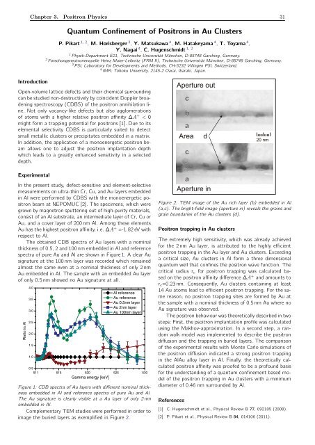
Figure 1: CDB spectra of Au layers with different nominal thickness<br />
embedded in Al and reference spectra of pure Au and Al.<br />
The Au signature is clearly visible at a Au layer of only 2 nm<br />
embedded in Al.<br />
Complementary TEM studies were performed in order to<br />
image the buried layers as exemplified in Figure 2.<br />
Aperture out<br />
c<br />
b<br />
a<br />
Area<br />
c<br />
b<br />
d<br />
a<br />
Aperture in<br />
20 nm<br />
Figure 2: TEM image of the Au rich layer (b) embedded in Al<br />
(a,c). The bright-field image (aperture in) reveals the grains and<br />
grain boundaries of the Au clusters (d).<br />
Positron trapping in Au clusters<br />
The extremely high sensitivity, which was already achieved<br />
for the 2 nm Au layer, is attributed to the highly efficient<br />
positron trapping in the Au layer and Au clusters. Exceeding<br />
a critical size, Au clusters in Al form a three dimensional<br />
quantum well that confines the positron wave function. The<br />
critical radius r c for positron trapping was calculated based<br />
on the positron affinity difference ∆A + and amounts to<br />
r c =0.23 nm. Consequently, Au clusters containing at least<br />
14 Au atoms lead to efficient positron trapping. For the same<br />
reason, no positron trapping sites are formed by Au at<br />
the sample with a nominal thickness of 0.5 nm Au where no<br />
Au signature was observed.<br />
The positron behaviour was theoretically descirbed in two<br />
steps: First, the psoitron implantation profile was calculated<br />
using the Makhov-approximation. In a second step, a random<br />
walk model was implemented to describe the positron<br />
diffusion and the trapping in buried layers. The comparison<br />
of the experimental results with Monte Carlo simulations of<br />
the positron diffusion indicated a strong positron trapping<br />
in the AlAu alloy layer in Al. Finally, the theoretically calculated<br />
positron affinity was proofed to be a profound basis<br />
for the understanding of a quantum confinement based model<br />
of the positron trapping in Au clusters with a minimum<br />
diameter of 0.46 nm surrounded by Al.<br />
References<br />
[1] C. Hugenschmidt et al., Physical Review B 77, 092105 (2008).<br />
[2] P. Pikart et al., Physical Review B 84, 014106 (<strong>2011</strong>).