ELECTRICAL CHARACTERISTICS OF LOW VOLTAGE ...
ELECTRICAL CHARACTERISTICS OF LOW VOLTAGE ...
ELECTRICAL CHARACTERISTICS OF LOW VOLTAGE ...

Create successful ePaper yourself
Turn your PDF publications into a flip-book with our unique Google optimized e-Paper software.
TIA PN-4584<br />
Revision 1.2<br />
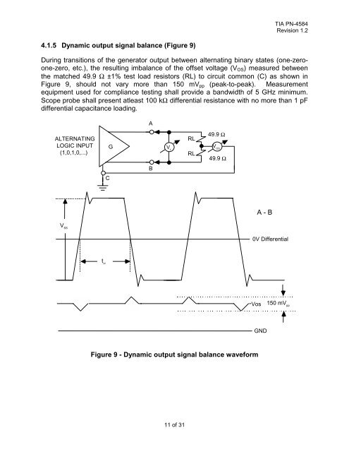
4.1.5 Dynamic output signal balance (Figure 9)<br />
During transitions of the generator output between alternating binary states (one-zeroone-zero,<br />
etc.), the resulting imbalance of the offset voltage (V OS ) measured between<br />
the matched 49.9 Ω ±1% test load resistors (RL) to circuit common (C) as shown in<br />
Figure 9, should not vary more than 150 mV pp (peak-to-peak). Measurement<br />
equipment used for compliance testing shall provide a bandwidth of 5 GHz minimum.<br />
Scope probe shall present atleast 100 kΩ differential resistance with no more than 1 pF<br />
differential capacitance loading.<br />
A<br />
ALTERNATING<br />
LOGIC INPUT<br />
(1,0,1,0,...)<br />
G<br />
V t<br />
RL<br />
RL<br />
49.9 Ω<br />
V OS<br />
49.9 Ω<br />
B<br />
C<br />
A - B<br />
V SS<br />
t ui<br />
0V Differential<br />
Vos<br />
150 mV pp<br />
GND<br />
Figure 9 - Dynamic output signal balance waveform<br />
11 of 31