ELECTRICAL CHARACTERISTICS OF LOW VOLTAGE ...
ELECTRICAL CHARACTERISTICS OF LOW VOLTAGE ...
ELECTRICAL CHARACTERISTICS OF LOW VOLTAGE ...

You also want an ePaper? Increase the reach of your titles
YUMPU automatically turns print PDFs into web optimized ePapers that Google loves.
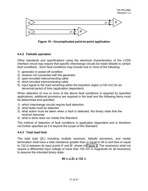
TIA PN-4584<br />
Revision 1.2<br />
G<br />
ZT<br />
R<br />
G<br />
ZT<br />
R<br />
Figure 19 - Uncomplicated point-to-point application<br />
4.4.2 Failsafe operation<br />
Other standards and specifications using the electrical characteristics of the LVDS<br />
interface circuit may require that specific interchange circuits be made failsafe to certain<br />
fault conditions. Such fault conditions may include one or more of the following:<br />
1) generator in power-off condition<br />
2) receiver not connected with the generator<br />
3) open-circuited interconnecting cable<br />
4) short-circuited interconnecting cable<br />
5) input signal to the load remaining within the transition region (±100 mV) for an<br />
abnormal period of time (application dependent)<br />
When detection of one or more of the above fault conditions is required by specified<br />
applications, additional provisions are required in the load and the following items must<br />
be determined and specified:<br />
1) which interchange circuits require fault detection<br />
2) what faults must be detected<br />
3) what action must be taken when a fault is detected; the binary state that the<br />
receiver assumes<br />
4) what is done does not violate this Standard<br />
The method of detection of fault conditions is application dependent and is therefore<br />
not further specified as it is beyond the scope of this Standard.<br />
4.4.3 Total load limit<br />
The total load (ZL) including multiple receivers, failsafe provisions, and media<br />
termination shall have a total resistance greater than or equal to 90 Ω and less or equal<br />
to 132 Ω between its input points A' and B', shown in Figure 2. The receiver(s) shall not<br />
require a differential input voltage of more than 100 mV in magnitude for all receiver(s)<br />
to assume the intended binary state.<br />
90 Ω ≤ ZL ≤ 132 Ω<br />
21 of 31