ELECTRICAL CHARACTERISTICS OF LOW VOLTAGE ...
ELECTRICAL CHARACTERISTICS OF LOW VOLTAGE ...
ELECTRICAL CHARACTERISTICS OF LOW VOLTAGE ...

You also want an ePaper? Increase the reach of your titles
YUMPU automatically turns print PDFs into web optimized ePapers that Google loves.
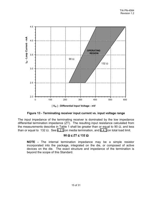
TIA PN-4584<br />
Revision 1.2<br />
4.5<br />
IID - Loop Current - mA<br />
4.0<br />
3.5<br />
90 Ω<br />
OPERATING<br />
REGION<br />
132 Ω<br />
3.0<br />
2.5<br />
2.0<br />
0<br />
100<br />
200<br />
300<br />
400<br />
500<br />
600<br />
| V ID | - Differential Input Voltage - mV<br />
Figure 13 - Terminating receiver input current vs. input voltage range<br />
The input impedance of the terminating receiver is dominated by the low impedance<br />
differential termination impedance (ZT). The resulting input resistance calculated from<br />
the measurements describe in Table 1 shall be greater than or equal to 90 Ω, and less<br />
than or equal to 132 Ω. See 4.2.5 on media termination, and 4.4.3 on total load limit.<br />
90 Ω ≤ ZT ≤ 132 Ω<br />
NOTE - The internal termination impedance may be a simple resistor<br />
incorporated into the package, integrated on the die, or composed of active<br />
devices on the die. The exact structure and impedance of the termination is<br />
beyond the scope of this Standard.<br />
15 of 31