ELECTRICAL CHARACTERISTICS OF LOW VOLTAGE ...
ELECTRICAL CHARACTERISTICS OF LOW VOLTAGE ...
ELECTRICAL CHARACTERISTICS OF LOW VOLTAGE ...

Create successful ePaper yourself
Turn your PDF publications into a flip-book with our unique Google optimized e-Paper software.
TIA PN-4584<br />
Revision 1.2<br />
3 APPLICABILITY<br />
3.1 General applicability<br />
The provisions of this Standard may be applied to the circuits employed at the interface<br />
between equipments where information being conveyed is in the form of binary signals.<br />
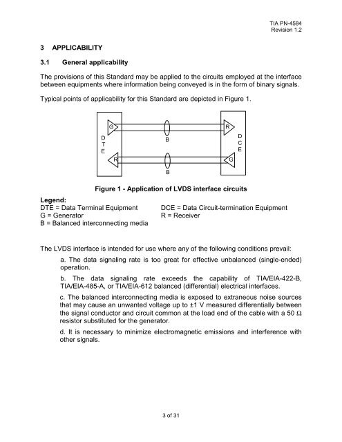
Typical points of applicability for this Standard are depicted in Figure 1.<br />
G<br />
R<br />
D<br />
T<br />
E<br />
R<br />
B<br />
G<br />
D<br />
C<br />
E<br />
B<br />
Figure 1 - Application of LVDS interface circuits<br />
Legend:<br />
DTE = Data Terminal Equipment DCE = Data Circuit-termination Equipment<br />
G = Generator<br />
R = Receiver<br />
B = Balanced interconnecting media<br />
The LVDS interface is intended for use where any of the following conditions prevail:<br />
a. The data signaling rate is too great for effective unbalanced (single-ended)<br />
operation.<br />
b. The data signaling rate exceeds the capability of TIA/EIA-422-B,<br />
TIA/EIA-485-A, or TIA/EIA-612 balanced (differential) electrical interfaces.<br />
c. The balanced interconnecting media is exposed to extraneous noise sources<br />
that may cause an unwanted voltage up to ±1 V measured differentially between<br />
the signal conductor and circuit common at the load end of the cable with a 50 Ω<br />
resistor substituted for the generator.<br />
d. It is necessary to minimize electromagnetic emissions and interference with<br />
other signals.<br />
3 of 31